Note: Descriptions are shown in the official language in which they were submitted.
84334807
HEATING ELEMENT FOR SENSOR ARRAY
[0001] This application claims priority to U.S. Provisional Application No.
62/276,561, filed January 8, 2016 and U.S. Provisional Application No.
62/356,629, filed
June 30, 2016.
BACKGROUND
[0002] This disclosure relates to a sensing device which allows for multiple
tests to
be run concurrently using a small sample volume.
SUMMARY OF THE INVENTIVE CONCEPT(S)
[0003] In the various illustrative embodiments herein, test devices are
described
with opposing sensor arrays, same side contacts, and integrated heating
elements.
[0003a] According to one aspect of the present invention, there is provided a
test
device comprising: a first planar substrate with a first planar surface; a
second planar substrate
with a second planar surface; a first sensing area and a second sensing area,
the first sensing
area and the second sensing area being disposed in between the first planar
surface and the
second planar surface, both of the first sensing area and the second sensing
area comprising a
chemical and/or reagent in electrical connection with a first electrode and a
second electrode,
respectively; a first planar intermediate isolating layer with a flow channel,
wherein the first
sensing area opposes the second sensing area with the flow channel disposed in
between the
first sensing area and the second sensing area; and a first heating element
disposed in between
the first planar surface and the second planar surface.
BRIEF DESCRIPTIONS OF THE DRAWINGS
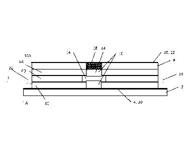
[0004] Fig. 1 depicts side view of a first embodiment of the low-volume
sensing
device.
[0005] Fig. 2 depicts a top view of the first embodiment of the low-volume
sensing
device.
1
CA 3010823 2019-07-05
84334807
[0006] Fig. 3 depicts an exploded side view of the first embodiment of the low-
volume sensing device.
[0007] Fig. 4 depicts an exploded perspective view of the first embodiment of
the
low-volume sensing device.
[0008] Fig. 5 depicts a side view of a second embodiment of the low-volume
sensing
device.
[0009] Fig. 6 depicts a top view of the second embodiment of the low-volume
sensing device.
[0010] Fig. 7 depicts an exploded side view of the second embodiment of the
low-
volume sensing device.
[0011] Figs. 8 and 9 illustrate a cross section view and a top view of a third
embodiment of the low-volume sensing device.
[0012] Figs. 10 and 11 illustrate a cross section view and a top view of a
fourth
embodiment of the low-volume sensing device.
DETAILED DESCRIPTION OF THE INVENTIVE CONCEPT(S)
[0013] Before explaining at least one embodiment of the inventive concepts
disclosed herein in detail, it is to be understood that the inventive concepts
are not limited in
their application to the details of construction and the arrangement of the
components or steps
or methodologies set forth in the following description or illustrated in the
drawings. The
inventive concepts disclosed herein are capable of other embodiments or of
being practiced or
carried out in various ways. Also, it is to be understood that the phraseology
and terminology
employed herein is for the purpose of description and should not be regarded
as limiting the
inventive concepts disclosed and claimed herein in any way.
[0014] In the following detailed description of embodiments of the inventive
concepts, numerous specific details are set forth in order to provide a more
thorough
understanding of the inventive concepts. However, it will be apparent to one
of ordinary skill
in the art that the inventive concepts within the instant disclosure may be
practiced without
these specific details. In other instances, well-known features have not been
described in
detail to avoid unnecessarily complicating the instant disclosure.
2
CA 3010823 2019-07-05
84334807
100151 As used herein, the terms "comprises," "comprising," "includes,"
"including,"
"has," "having" or any other variation thereof, are intended to cover a non-
exclusive inclusion.
For example, a composition, a process, method, article, or apparatus that
comprises a list of
elements is not necessarily limited to only those elements but may include
other elements not
expressly listed or inherently present therein.
100161 As used herein the terms "approximately," "about," "substantially" and
variations thereof are intended to include not only the exact value qualified
by the term, but to
also include some slight deviations therefrom, such as deviations caused by
measuring error,
manufacturing tolerances, wear and tear on components or structures, settling
or precipitation
of cells or particles out of suspension or solution, chemical or biological
degradation of
solutions over time, stress exerted on structures, and combinations thereof,
for example.
[0017] As used herein, the term "sample" and variations thereof is intended to
include
biological tissues, biological fluids, chemical fluids, chemical substances,
suspensions,
solutions, slurries, mixtures, agglomerations, tinctures, slides, powders, or
other preparations
of biological tissues or fluids, synthetic analogs to biological tissues or
fluids,
2a
CA 3010823 2019-07-05
CA 03010823 2018-07-06
WO 2017/120464
PCMJS2017/012526
bacterial cells (prokaryotic or eukaryotic), viruses, single-celled organisms,
lysed biological
cells, fixed biological cells, fixed biological tissues, cell cultures, tissue
cultures, genetically
engineered cells and tissues, genetically engineered organisms, and
combinations thereof, for
example.
[0018] Unless expressly stated to the contrary, "or" refers to an inclusive or
and not
to an exclusive or. For example, a condition A or B is satisfied by anyone of
the following: A
is true (or present) and B is false (or not present), A is false (or not
present) and B is true (or
present), and both A and B are true (or present). An inclusive or may be
understood as being
the equivalent to: at least one of condition A or B.
[0019] In addition, use of the "a" or "an" are employed to describe elements
and
components of the embodiments herein. This is done merely for convenience and
to give a
general sense of the inventive concepts. This description should be read to
include one or at
least one and the singular also includes the plural unless it is obvious that
it is meant
otherwise.
[0020] As used herein any reference to "one embodiment" or "an embodiment"
means that a particular element, feature, structure, or characteristic
described in connection
with the embodiment is included in at least one embodiment. The appearances of
the phrase
"in one embodiment" in various places in the specification are not necessarily
all referring to
the same embodiment.
[0021] Finally, the embodiments of the low-volume sensing device disclosed
herein may be understood with reference to a first, second, and third
direction such as, for
example, lateral direction 'A', a longitudinal direction 1' which is
perpendicular to lateral
direction 'A', and a transverse direction 'T' which is perpendicular to
longitudinal direction
'L.' The longitudinal direction L and the lateral direction A extend
horizontally as illustrated,
and the transverse direction T extends vertically, though it should be
appreciated that these
directions may change depending, for instance, on the orientation of the low-
volume sensing
device. It should also be understood that first direction may be referred to
as the lateral
direction. It should also be understood that second direction may be referred
to as the
longitudinal direction. It should also be understood that third direction may
be referred to as
the transverse direction.
[0022] The inventive concepts disclosed herein are generally directed to the
need to
minimize the sample volume required to test two or more analytes concurrently.
Low sample
volumes are desirable when the sample is limited, such as in the case of whole
blood from
neonatal patients, or when the sample itself is expensive. As opposed to prior
art test devices
3
CA 03010823 2018-07-06
WO 2017/120464
PCT/1JS2017/012526
configurations, which required the volume to increase with the number of
analytes being
detected, the required sample volume can be greatly reduced when the two co
planar arrays of
sensors are arranged in such a way that they are facing one another in a
sandwich
configuration (also referred to as an opposing sensor array) as opposed to a
configuration in
which each sensor is arranged in a coplanar configuration. In order to
simplify the manner in
which test devices with opposing sensor arrays interface with medical
instruments, the testing
device can be configured such that its electrical contacts can be easily
accessed. This
configuration maximizes the number of sensors that can be incorporated into a
single test
device while simplifying the manner in which the device interfaces with the
medical
instrument.
[0023] Illustrative embodiments of low-volume testing devices with opposing
sensor arrays are discussed in connection with Figs. 1 through 7 below. It
should be
understood that the term "test device," and variations thereof, include single
use or multi use
devices as well as disposable "test strips."
[0024] Figs. 1-4 depict a first embodiment a low-volume sensing device. Fig. 1
depicts side view of a first embodiment of the low-volume sensing device along
line Y-Y'
from Fig. 4. Fig. 2 depicts a top view of the first embodiment of the low-
volume sensing
device. Fig. 3 depicts an exploded side view of the first embodiment of the
low-volume
sensing device along line Y-Y' from Fig. 4. Fig. 4 depicts an exploded
perspective view of
the first embodiment of the low-volume sensing device.
[0025] Test device 100 contains a first planar substrate 2. Planar substrate 2
may be
substantially planar with a substantially planar upper surface and
substantially planar lower
surface of the planar substrate 2¨both of which extend in the lateral
direction A and the
longitudinal direction L (as shown in Fig. 2) and are separated by a thickness
extending along
the transverse direction T.
[0026] Test device 100 further includes planar conductive layer 4 disposed on
or
adjacent to the upper surface of planar substrate 2. Stated differently,
conductive layer 4 is
disposed above planar substrate 2 along the transverse direction T and is
coplanar with the
upper surface of planar substrate 2. While conductive layer 4 includes one or
more individual
coplanar electrodes 20, as shown in Fig. 4, conductive layer 4 is represented
by the
designated shaded area in Fig. 2. Coplanar electrodes 20 may be formed using a
variety of
methods and materials known to a person of ordinary skill in the art. For
example, coplanar
electrodes 20 may be formed using a thick film approach (e.g., screen
printing, rotogravure,
pad printing, stenciling, ink jetting or aerosol jetting conductive material
such as carbon, Cu,
4
CA 03010823 2018-07-06
WO 2017/120464
PCMJS2017/012526
Pt, Pd, Au, and/or Nanotubes (such as carbon nanotubes), etc..,) or a thin
film approach (e.g.,
by sputtering, thermal spraying, and/or cold spraying conductive material).
Coplanar
electrodes 20 may be partitioned using, for example, laser ablation. It should
be understood
that the configuration of electrodes 20 depicted herein are merely for
illustrative purposes
only and a person of ordinary skill in the art will appreciate that electrodes
20 may be
distributed on substrate 2 in a variety of ways. As will be appreciated by
those skilled in the
art, the term "coplanar," as used herein to describe electrodes 20, should be
understood as
encompassing those electrodes which are substantially coplanar (as well as
those which are
fully co planar. Thus, individual electrodes 20 can be slightly raised,
recessed, and/or angled
as compared other coplanar electrodes 20 on planar substrates 2 and still be
considered
coplanar.
[0027] Test device 100 additionally includes a second planar substrate 8,
which is
structurally similar to planar substrate 2, disposed above the first
conductive layer 4 along the
transverse direction T. Planar substrate 8 may be substantially planar with a
substantially
planar upper surface and substantially planar lower surface of the planar
substrate 8 both of
which extend in the lateral direction A and the longitudinal direction L (as
shown in Fig. 2)
and are separated by a thickness extending along the transverse direction T.
Planar substrate
8 contains conductive vias 18 (otherwise known as filled vias) which extend
between the
upper and lower surfaces of planar substrate 8. Planar substrates 2 and 8 may
be formed
using a variety of methods and materials known to a person of ordinary skill
in the art. For
example, planar substrate 2 may be flexible or rigid and may be constructed
using, for
example, standard PCB, flex PCB, PET, PI, ceramic, glass, etc. For example,
planar
substrate 2 may be made out of an inert substrate such as a dielectric,
pressure sensitive
adhesive, laminate, etc...
[0028] Test device 100 further includes one or more immediate layers 6
disposed in
between conductive layer 4 and second planar substrate 8 (e.g., above and
adjacent to planar
conductive layer 4 and below and adjacent to second planar substrate 8 along
transverse
direction T). Similar to planar substrates 2 and 8, intermediate layers 6 may
be substantially
planar with a substantially planar upper surface and substantially planar
lower surface of the
intermediate layer 6¨both of which extend in the lateral direction A and the
longitudinal
direction L (as shown in Fig. 2) and are separated by a thickness extending
along the
transverse direction T. The intermediate layer(s) 6 may be formed using a
variety of methods
and materials known to a person of ordinary skill in the art. For example,
intermediate layers
6 may be made out of an inert substrate such as a dielectric, pressure
sensitive adhesive,
CA 03010823 2018-07-06
WO 2017/120464
PCMJS2017/012526
laminate, etc... Alternatively, intermediate layers 6 can be integrated into
one or both of
planar substrate 8 and conductive layer 4 by forming intermediate layer(s) 6
directly on the
upper surface of conductive layer 4 or the lower surface of substrate 8. One
or more of
intermediate layer(s) 6 can be an isolating layer(s) made from a dielectric or
insulating
material which isolates one or more, up to all, of electrodes 20 from one or
more, up to all, of
conductive vias 18. Alternatively, intermediate layers 6 can provide
conductive pathways
which allow one or more, up to all. electrodes 20 and conductive vias 18 to be
electrically
connected to one another.
[0029] In the embodiment depicted in in Figs. 1-4, test device 100 contains an
intermediate layer 6B which defines a fluid flow channel 14. The flow channel
14 allows
fluid to flow from an inlet to the outlet of the flow channel 14.
[0030] Test device 100 may also contain intermediate layers 6A and 6C disposed
on
opposing planar sides of the intermediate layer 6B. Intermediate layers 6A and
6C may
define one or more sensing areas 16. Individual sensing areas 16 allow fluid
traveling
through the fluid flow channel 14 to come into contact with individual
coplanar electrodes 20
of conductive layer 4 and conductive vias 18 of the second substrate layer 8,
respectively.
For example, the sensing areas 16 depicted in Figures 1-4 are circular
apertures (which can
also be referred to as reaction wells) which extend through the respective
intermediate layers
6A and 6C. Sensing areas 16 may also be fully or partially filled with a
chemical/reagent 24
which may react with fluid in the fluid flow channel 14 and produce a
detectable analyte. In
certain embodiments, intermediate layer 6C can function as a masking layer by
protecting
conductive layer 4 from damage during the fabrication process and by defining
sensing areas
16. Alternatively, individual sensing areas 16 may also be defined without the
need for
intermediate layers 6A and 6C by applying chemicals and/or reagents directly
on one or both
of coplanar electrodes 20 and conductive vias 18 on the first or the second
planar substrate 2
and 8, respectively. It should also be appreciated that one or both of
intermediate layers 6A
and 6C may be combined with intermediate layer 6B to form a combined
intermediate layer
which defines both a fluid flow channel 14 and one or more sensor areas 16.
[0031] Test device 100 further includes planar conductive layer 10 disposed on
or
adjacent to the upper surface of planar substrate 8. Stated differently,
conductive layer 10 is
disposed above planar substrate 8 along the transverse direction T and is
coplanar with the
upper surface of planar substrate 8. While conductive layer 10 includes one or
more
individual coplanar electrodes 22, as shown in Fig. 4, conductive layer 10 is
represented by
the designated shaded area in Fig. 2. Coplanar electrodes 22 may be formed and
partitioned
6
CA 03010823 2018-07-06
WO 2017/120464
PCMJS2017/012526
using a variety of methods and materials known to a person of ordinary skill
in the art¨such
as those identified above with respect to coplanar electrodes 20. One or more,
up to all, of
coplanar electrodes 22 are in electrical contact with at least one respective
conductive via 18
in planar substrate 8¨thus allowing reactions taking place in the sensing area
16 to be
detected by a medical device electrically coupled to coplanar electrode(s) 22.
[0032] As best shown in Fig. 1, sensing areas 16 in intermediate layer 6A
opposes
(i.e., is opposite) those sensing areas 16 in intermediate layer 6C with the
flow channel 14 of
intermediate layer 6B disposed in between. In this opposed configuration,
sensing areas 16 in
intermediate layer 6A face those sensing areas 16 in intermediate layer 6C.
Stated differently,
sensing areas 16 in intermediate layer 6C is disposed below the sensing area
16 in
intermediate layer 6A along a line extending from the first planar substrate 2
to the second
planar substrate 8 with the flow channel located in between the respective
sensing areas 16 of
intermediate layers 6A and 6C.
[0033] As illustrated in, for example, Figs. 1 and 2, intermediate layers 6,
dielectric
layer 8, and conductive layer 10 are arranged such than an uncovered portion
26 of the first
conductive layer 4 is visible when viewing the testing device 100 from above
conductive
layer 10 along the transverse direction T. For example, uncovered portion 26
may be visible
from above because (1) one or more, up to all, of the intermediate layers 6,
dielectric layer 8,
and conductive layer 10 may have an area in the lateral direction A and the
longitudinal
direction L that is smaller than the area of the conductive layer 4, and/or
(2) one or more, up
to all, of the intermediate layers 6, dielectric layer 8, and conductive layer
10 are offset in one
or both of the lateral direction A and the longitudinal direction L as
compared to the
conductive laver 4. The uncovered portion 26 of conductive layer 4 is disposed
within the
area indicated and has an area (in the lateral direction A and the
longitudinal direction L) that
is smaller than the comparative area of the entire conductive layer 4. It
should also be
understood that while the conductive layer 4 has two distinct uncovered
portions 26 in Figs. 1
and 2 (located on opposite edges of the testing device 100), other embodiments
of the
concepts herein may include one, two, three or more uncovered portions 26
located, for
example, one or more, up to all, of the edges of conductive layer 4.
[0034] Continuing with Figs. 1 and 2, because the uncovered portion 26 of
conductive layer 4 and conductive layer 10 are both visible when viewing the
testing device
100 from above conductive layer 10 along the transverse direction T, the
electrodes 20 and 22
located thereon can be accessed from the top of the device. These "top side"
electrical
contacts can be easily accessed by an associated medical instrument.
7
CA 03010823 2018-07-06
WO 2017/120464
PCMJS2017/012526
[0035] In yet another alternative embodiment of test device 100, the
conductive
layer 10, second substrate layer 8, and intermediate layer 6C of test device
100 can be
replaced by a lid layer that is devoid of electrodes, vias, or sensing areas.
Thus exposed areas
26 of conductive layer 4 would be the only conductive layer visible from the
above the test
device 100. Alternatively, such a lid layer may be placed on top of conductive
layer 10.
This lid layer is similar to the second substrate layer 8' discussed below
with respect to Fig.s
5-7.
[0036] Figs. 5-7 depict a second embodiment a low-volume test device 100'.
Fig. 5
depicts a side view of a second embodiment of the low-volume sensing device.
Fig. 6 depicts
a top view of the second embodiment of the low-volume sensing device. Fig. 7
depicts an
exploded side view of the second embodiment of the low-volume sensing device.
In the
following description of test devices 100', it should be noted that similar
reference numbers
to those used to describe test device 100 in Figs. 1-4 are intended to refer
to similar features
(unless stated otherwise)¨thus avoiding the need to duplicate the detailed
description of
those features.
[0037] As best shown in Fig. 5, test device 100' has a first planar substrate
2', a first
conductive layer 4', and an intermediate layers 6A', 6B', and 6C'. Test device
100' further
comprises a second conductive layer 10' disposed on or adjacent to the upper
surface of
intermediate layer 6C' along the transverse direction T, as opposed to the
position of
conductive layer 10 in Figs. 1-4. As with conductive layer 10, while
conductive layer 10'
includes one or more individual coplanar electrodes 22', conductive layer 10'
is generally
represented by the designated shaded area in Fig. 6. One or more, up to all,
of coplanar
electrodes 22' are in electrical contact with at least one respective sensing
area 16' in
intermediate layer 6C'¨thus allowing reactions taking place in the sensing
area 16' to be
detected by a medical device electrically coupled to coplanar electrode(s)
22'.
[0038] Test device 100' further includes a substrate layer 8'disposed on or
adjacent
to the upper surface of the second conductive layer 10' along the transverse
direction T.
Planar substrates 2' and 8' may be formed using a variety of methods and
materials known to
a person of ordinary skill in the art. For example, planar substrate 2' or 8'
may be flexible or
rigid and may be constructed using, for example, standard PCB, flex PCB, PET,
PI, ceramic,
glass, etc. For example, planar substrate 2' or 8. may be made out of an inert
substrate such
as a dielectric, pressure sensitive adhesive, laminate, etc... In one
embodiment, substrate 8'
may be a simple laminate layer which acts as a cover, thereby protecting the
individual
electrodes 22' from accidental damage.
8
CA 03010823 2018-07-06
WO 2017/120464
PCMJS2017/012526
[0039] As illustrated in, for example, Figs. 5 and 6, second planar substrate
8' in
test device 100' is configured such than an uncovered portion 28 of the second
conductive
layer 10' is visible when viewing the testing device 100' from above second
conductive layer
4' along the transverse direction T. For example, uncovered portion 28 may be
visible from
above because (1) second planar substrate 8' has an planar area in the lateral
direction A and
the longitudinal direction L that is smaller than the planar area of the
conductive layer 10,
and/or (2) second planar substrate 8'is offset in one or both of the lateral
direction A and the
longitudinal direction L as compared to the conductive layer 10'. The
uncovered portion 28
of second conductive layer 10' is disposed within the area indicated and has
an area (in the
lateral direction A and the longitudinal direction L) that is smaller than the
comparative area
of the entire conductive layer 4. It should also be understood that while the
second
conductive layer 10 has two distinct uncovered portions 28 in Figs. 5 and 6
(located on
opposite edges of the testing device 100'), other embodiments of the concepts
herein may
include one, two, three or more uncovered portions 28 located, for example,
one or more, up
to all, of the edges of conductive layer 10'.
[0040] Thermal control of these opposing sensor arrays can be achieved with
the
use of a thermal heating element. Examples of heating elements include, but
are not limited
to, heating circuitry (e.g., wires) and/or a heating block. The thermal
heating element may be
placed in contact with the 'backside' of test devices or otherwise integrated
into the
substrate(s) upon which a coplanar sensor array is positioned. For example, in
the
embodiments shown above the heating element can be integrated into planar
substrates 2
and/or 8 or placed on the -backside" thereof (i.e., the surface of planar
substrates 2 and/or 8
opposite the flow channel 14). However, when the heating element is integrated
in the
substrate or position on the backside of the test device, thermal control of
the test device as a
whole is dependent upon the thermal characteristics (e.g., the thermal
conductivity) of the
substrate material itself.
[0041] In accordance with the inventive concepts described herein an
alternative
heating configuration is proposed which allows for more accurate and precise
heating control
of test devices. Rather than integrating the heating element into or on the
backside of a
substrate, the heating element can be used to define, in whole or in part,
flow channel 14.
Turning to the Figures, a heating element can be incorporated into one, two,
or all three
intermediate layers 6A, 6A', 6B, 6B', 6C, and 6C' of the above Figures.
[0042] According to one embodiment, variations of the embodiments shown in
Figs. 1-4 and 5-7 contain one or more intermediate layers 6 into which a
heating element(s)
9
CA 03010823 2018-07-06
WO 2017/120464
PCMJS2017/012526
are integrated. By integrating heating elements into one or more intermediate
layers 6 a type
of "heating gasket" is formed which not only defines¨at least in part¨the flow
channel 14
but also helps to create a seal to help prevent the liquid sample from
escaping the flow
channel 14. Similar to the above discussion, intermediate layers 6 with an
integrated heating
element may be made out of an inert substrate such as a dielectric, pressure
sensitive
adhesive, laminate, etc... The material used for the intermediate layers 6 may
selected based
on its thermal characteristics. For example, materials with better heat
transfer properties may
be preferred over those that are more difficult to control.
[0043] Figs. 8 and 9 illustrate a cross section view and a top view of test
device
200. As noted by the similarly numbered elements and discussed below, test
device 200
contains many of the same components as those described above with respect to
test device
100 only arranged in a slightly difference configuration. Notably, test device
200 contains
one or more sensing areas 16" disposed on a respective surface of substrates
2" and 8" which
oppose (e.g., face) one another with a flow channel 14" disposed there
between. Sensing area
16" may, for example, be chemicals/reagents 24" disposed on a surface of
substrate 2" and 8"
(by, for example, printing or drying in place) which react with analytes in
sample in the fluid
flow channel 14" and produce a detectable signal. The detectable signal is
measured via the
combination of the sensing area 16", the coplanar electrodes 20" and 22"
located underneath
the sensing area 16". Test device 200 also contains a single intermediate
layer 6B" which
defines, in whole or in part, the flow path 14" and contains one or more
heating element
integrated therein. Stated another way, optional intermediate layers 6A and 6C
from test
device 100 have been removed and the reagents 24" have been disposed directly
onto
substrates 2" and 8"¨and not in intermediate layers 6A, 6C. Additionally, a
conductive
layer 10" is located on a surface of substrate 8" opposite the flow channel 14-
but electrically
coupled to those electrodes disposed on the opposite surface of the substrate
8".
[0044] Figs. 10 and 11 illustrate a cross section view and a top view of test
device
200. As noted by the similarly numbered elements and discussed below, test
device 200
contains many of the same components as those described above with respect to
test device
100' only arranged in a slightly difference configuration. Notably, test
device 200 contains
one or more sensing areas 16" disposed on a respective surface of substrates
2¨ and 8"
which oppose (e.g., face) one another with a flow channel 14¨ disposed there
between.
Sensing area 16". may, for example, be chemicals/reagents 24-' disposed on a
surface of
substrate 2¨ and 8" (by, for example, printing or drying in place) which react
with analytes
in the sample fluid in the fluid flow channel 14" and produce a detectable
signal. The
CA 03010823 2018-07-06
WO 2017/120464
PCMJS2017/012526
detectable signal is measured via the combination of the sensing area 16" and
the coplanar
electrodes 20" located underneath the sensing area 16". Test device 200 also
contains a
single intermediate layer 6B¨ which defines, in whole or in part, the flow
path 14" and
contains one or more heating element integrated therein. Stated another way,
optional
intermediate layers 6A' and 6C' from test device 100' have been removed and
the reagents
24" have been disposed directly onto substrates 2" and 8"¨and not in
intermediate layers
6A', 6C'.
[0045] While not shown, heating elements may be disposed adjacent to one or
both
of substrates 2, 8 and between the flow channel and a substrate 2, 8. In this
embodiment the
heating element forms an addition layer between the substrate 2, 8 and the
intermediate
layer(s) 6. An additional insulating laver may also be positioned between the
heating element
and the substrate so as to minimize the effects of the substrate's thermal
characteristics. It is
worth noting that a sensor device may have two or more heating elements ¨ one
or more of
which are positioned between substrate 2, 8 and the intermediate layer(s) 6
and others
integrated into intermediate layer(s) 6.
[0046] By integrating the heating element either (1) between a respective
substrate
2, 8 or (2) into intermediate layer(s) 6 so as to define, at least in part,
the flow channel 14,
several design advantages are achieved over a substrate with a heating element
integrated into
a substrate or positioned on the backside. Examples of such advantages are:
sample flowing
through the flow channel 14 can be more efficiently heated¨which means liquid
can flow
through the sensor faster. Additionally, the temperature can be more precisely
controlled
when the flow channel is heated directly as opposed to have to account for the
thermal
characteristics (e.g., the thermal conductivity) of the substrate material
itself Lastly, in the
opposing configuration depicted in the Figures, a heating element(s) can be
located in one
position (e.g., in intermediate layer(s) 6) as opposed to two separate
locations ¨one on the
backside of each planar substrates 2 and 8, respectively.
[0047] A person of ordinary skill in the art should also appreciate that there
are a
variety of methods which may be used to manufacture the test device 100, 100',
200, and
200', as described above. Furthermore, person of ordinary skill in the art
should further
appreciate that a variety of medical instruments can be adapted to interface
with testing
devices with top side contacts, such as testing devices 100, 100', and 100'.
[0048] It should be appreciated that the inventive concepts disclosed herein
can be
incorporated into alternative configurations of test device 100. For example,
in an alternative
configuration of test device 100 layer 6B may be covered by a single 'cover'
layer rather than
11
CA 03010823 2018-07-06
WO 2017/120464
PCMJS2017/012526
those layers shown above layer 6B along the transverse direction T.
Furthermore, conductive
layers 4 and 10 in Figs. 1-7 are for illustrative purposes only and
alternative configurations of
test device 100 may vary the position and/or the features of conductive layers
in 4 and 10
without deviating from the intent of the inventive concepts discloses herein.
12