Note: Descriptions are shown in the official language in which they were submitted.
CA 03014303 2018-08-10
1
Soldering Tip for a Soldering Iron
The invention relates to a soldering tip for a soldering iron and its use in
the production of
a pane with an electrical connection element.
Window panes, in particular vehicle panes are frequently equipped with
electrically
conductive structures. Examples of such conductive structures are printed
heating
conductors or antennas. For connection to the necessary voltage source or
transmitting or
receiving unit, electrical connection elements are typically soldered on a
region of the
conductive structure, which is or can be connected to an electrical connection
cable.
A variety of different types of connection elements are known. US 6249966 B1 ,
US 2007/0224842 Al, and W02013/182394 Al disclose connection elements that are
implemented as snaps. These connection elements have the advantage of a
convenient
and reversible connection to the connection cable. Typically, the male snap is
soldered on
the pane and the female snap is provided with the connection cable. Male and
female
snaps can be connected to one another simply as intended in order to establish
the
electrical contact.
WO 2014/040773 Al discloses a connection element crimped around the connection
cable, wherein the crimp is soldered directly onto the conductive structure.
The soldering of connection elements can be automated using soldering robots.
Alternatively, however, the connection elements can also be hand soldered,
which is
economically viable in particular in low-wage countries and with relatively
small lots. In
hand soldering, controllable or non-controllable soldering irons, typically
equipped with
interchangeable soldering tips, are used. The soldering tip is brought into
contact with the
connection element, whereupon it transfers the heat generated by the soldering
iron via
the connection element to the soldering compound, which is fuzed thereby. For
this,
soldering tips must have high thermal conductivity and are typically made of
copper.
Commonly used soldering tips are shaped chisel-like with an elongated pointed
end
portion for contacting the connection element. In addition, rod electrodes
with a flat end
portion for contacting the connection element are commonly used as soldering
tips.
In hand soldering, care must be taken that the soldering tip has good contact
that is as
extensive as possible with the connection element in order to ensure efficient
energy input.
CA 03014303 2018-08-10
2
This places high demands on the careful work of the technician. In addition,
during hand
soldering, it is often necessary to specifically fix the connection element in
place to ensure
its stable positioning. The reason for this is the locally very limited
introduction of energy
with conventional soldering tips that require very high energy input to fuze
the entire solder.
The soldering compound must, consequently, be strongly heated and, as a
result, solidifies
only very slowly such that the connection element floats, so to speak, on the
soldering
compound and its position can change.
The object of the present invention is to provide an improved soldering tip
for a soldering
iron, in particular a hand-held soldering iron and an improved method executed
therewith
for producing a pane with an electrical connection element. The soldering tip
should, in
particular, ensure homogeneous energy input and enable more convenient
soldering as
well as making separate fixing of the connection element during the soldering
operation
unnecessary.
The object is accomplished according to the invention by a soldering tip in
accordance
with independent claim 1. Preferred embodiments emerge from the subclaims.
The soldering tip according to the invention for a soldering iron is intended
for soldering
an electrical connection element to an electrically conductive structure on a
substrate, in
particular on a window pane made of glass. The soldering tip comprises an end
portion on
the end of the soldering tip facing away from the soldering iron, which is
intended for
contacting the item to be soldered, in particular the connection element,
during the
soldering operation.
According to the invention, said end portion is substantially hemispherical.
This enables
efficient and simplified hand soldering of suitable connection elements, in
particular
connection elements with a central depression. The end portion in the shape of
a
hemisphere can be introduced into the depression such that an extensive area
of the
connection element, namely the area surrounding the depression, can be brought
reproducibly into contact with the soldering tip. Thus, efficient and
homogeneous energy
input is achieved, which results in uniform fuzing of the soldering compound.
The
hemispherical shape of the end portion of the soldering tip additionally
simplifies the
soldering, since less care is required in terms of the positioning of the
soldering iron. The
soldering iron can be held perpendicular to the substrate or even obliquely ¨
the
CA 03014303 2018-08-10
3
hemispherical shape ensures a reproducible contact area between the soldering
tip and
the connection element.
The soldering iron is equipped with heating means to heat the soldering tip.
The
temperature is transferred from the soldering tip to the soldering compound,
which is fuzed
thereby. This type of soldering iron is referred to in the technical jargon as
a "hot iron".
Said soldering iron is advantageously a hand-held soldering iron. The
soldering tip
according to the invention demonstrates its advantages in particular in hand
soldering.
Here, the precise positioning of the soldering iron is not completely
reproducible, which is
compensated by the contact area between the soldering tip of the connection
element
independently of the working angle. In contrast, however, the soldering tip
requires very
accurate local positioning relative to the connection element in order to
fully contact the
contact area. Tolerances in terms of the positioning of the connection element
can be
readily compensated during hand soldering such that the soldering tip can be
very simply
positioned with the required accuracy relative to the connection element. In
the case of
automated soldering, the position of the soldering tip is usually invariable
such that the
required adaptation to the precise position of the connection element in
production
tolerances is less simple.
The soldering tip is preferably an interchangeable soldering tip for a
soldering iron. Such
a soldering iron can be divided conceptually into three portions:
- an end portion for contacting the item to be soldered,
- a connection portion for connecting the soldering tip to the soldering iron,
- a middle portion, which extends between the end portion and the connection
portion.
The design of the connection portion is substantially defined by the type of
soldering iron
with which the soldering tip is to be used and, consequently, must be
compatible. In
principle, many connection systems are conceivable. Examples for this are plug-
in
connections, in which the end portion is inserted into a hole in the soldering
iron and is
fixed there, for example, by a magnet. Bayonet connections and screw
connections, in
which the end portion is provided with a thread or with holes through which
the attachment
screws can be guided.
In a preferred embodiment, the connection portion is widened compared to the
middle
portion such that the soldering tip can be secured on the soldering iron by
means of a
CA 03014303 2018-08-10
4
union nut. The union nut is screwed onto the soldering iron, which must, of
course, be
provided with a thread for this, and presses the widened connection portion
against the
soldering iron, by which means the soldering tip is securely fixed. The
connection portion
preferably has a flat connection surface on the side facing away from the
middle portion,
which is brought into contact with a corresponding flat connection surface of
the soldering
iron. The connection surfaces of the connection portion of the soldering tip
and of the
soldering iron are preferably congruent and are arranged congruently. With the
use of a
suitable union nut, it is, however, in principle, also possible to design the
contact surface
of the soldering tip smaller than the contact surface of the soldering iron.
The widening of
the connection portion compared to the middle portion is preferably at least 1
mm,
particularly preferably at least 2 mm, to ensure a stable connection to the
soldering iron.
In another preferred embodiment, the end portion of the soldering tip is
suitable for
insertion (plugging in) in the soldering iron. The soldering tip can be
secured in the
soldering iron, for example, with a laterally inserted screw. The end portion
has, in a
preferred embodiment, the same width as the middle portion.
The middle portion is preferably implemented in the shape of a right circular
cylinder as
this shape is, for one thing, customary for soldering tips and, for another,
the cross-section
of the middle portion corresponds to the cross-section of the hemispherical
end portion,
as a result of which the shapes are optimally matched, in particular if the
circular cylinder
has the same radius as the hemispherical end portion. However, in principle,
other shapes
of the middle portion are also conceivable, for example, with a square,
rectangular,
triangular, or polygonal cross-section.
The middle portion can be straight or also angled.
The soldering tip should have high thermal conductivity. The soldering tip
preferably
contains copper and is particularly preferably made of copper or of a copper-
containing
alloy, such as brass or bronze alloys, for example, nickel silver or
constantan. Copper has
high conductivity and is relatively economical. In principle, however, other
metals or alloys
are also suitable as material for the soldering tip.
The soldering tip can be provided with a coating to optimize its properties.
Thus, it is not
the core material of the soldering tip, preferably copper, that comes into
contact with the
item to be soldered; but rather the coating, which can, consequently, also be
referred to
CA 03014303 2018-08-10
as a contact layer or wetting layer. The contact layer forms the outer surface
of the
soldering tip.
In an advantageous embodiment, the soldering tip is nickel plated, i.e., has a
contact layer
based on nickel, preferably made of nickel. The nickel contact coating slows
transfer of
heat from the soldering tip to the item to be soldered. Thus, scaling of the
soldering tip,
which can occur in particular with the use of copper, can be avoided. The
thickness of the
nickel layer is preferably from 5 pm to 30 pm, particularly preferably from 10
pm to 15 pm.
In an alternative embodiment, the soldering tip is hard chrome plated. In the
context of the
invention, the term "hard chrome plating" refers to a contact layer based on
chromium,
preferably made of chromium, with a thickness of at least 1 pm. The chromium
contact
layer preferably has a layer thickness from 10 pm to 80 pm, particularly
preferably from
20 pm to 50 pm. Another layer, for example, a nickel layer with a thickness
from 5 pm to
pm, can be arranged underneath the chromium contact layer. The hard chrome
plating
increases the surface hardness and, in particular, the surface tension of the
soldering tip
such that undesirable wetting of the soldering tip with uncontrolled
outflowing soldering
compound is prevented.
The geometric dimensions of the soldering tip depend in particular on the
design of the
soldering iron used and the desired soldering tip temperature and can be
appropriately
selected by the person skilled in the art according to the requirements of the
intended use.
The overall length of the soldering tip is, for example, from 10 mm to 120 mm,
preferably
from 15 mm to 90 mm, in particular from 15 to 60 mm. Such a soldering tip is
easy to
handle and is heated adequately quickly and efficiently even in the end
portion.
The radius of the hemispherical end portion (also corresponds to the length
and width of
the end portion) is, for example, from 1 mm to 20 mm, preferably from 3 mm to
15 mm,
particularly preferably from 4 mm to 10 mm. The width of the middle portion is
preferably
in the same ranges and is particularly preferably the same as the radius of
the end portion.
The length of the middle portion is, in principle, limited only by the
handling properties and
the thermal conductivity of the soldering tip material. It is, for example,
from 1 mm to 100
mm, preferably from 5 mm to 80 mm. The width of the connection portion depends
on the
soldering iron used and is, for example, from 1 mm to 30 mm, preferably from 4
mm to 20
mm. In an advantageous embodiment, the width of the connection portion
corresponds to
the width of the connection surface of the soldering iron. The length of the
connection
CA 03014303 2018-08-10
6
portion is preferably from 1 mm to 10 mm, in particular from 1 mm to 5 mm in
the flange-
like connection variant with a widened connection portion. The length of the
connection
portion is preferably from 10 mm to 100 mm, in particular from 20 mm to 80 mm
in the
connection variant with a plug-in connection portion.
The invention also includes a soldering iron, in particular a hand-held
soldering iron, which
is equipped with the soldering tip according to the invention and can be
connected to a
voltage source. The invention also includes in particular a soldering station,
comprising a
soldering iron equipped with the soldering tip according to the invention and
a control unit
connected thereto via a cable, which control unit can be connected to a
voltage source.
The invention further includes a method for producing a pane with an
electrical connection
element, comprising
(a) providing a substrate,
(b) applying an electrically conductive structure on a region of the
substrate,
(c) arranging a soldering compound on a region of the electrically
conductive structure
and an electrical connection element on the soldering compound,
(d) soldering the connection element with a soldering iron having a soldering
tip
according to the invention.
The soldering iron is in particular a hand-held soldering iron, with which the
connection
element is hand soldered.
A major advantage of the soldering tip according to the invention consists in
very
homogeneous energy input, which is ensured by the reliable contacting of the
areas of the
connection element surrounding the depression. This results in the fact that,
overall, a
lower energy input is necessary to fuze the entire soldering compound. The
soldering
compound thus has a low temperature and cools more rapidly to the
solidification
temperature. Shifting of the connection element on the liquid soldering
compound can thus
be avoided, for which reason no additional measures for securing a connection
element
have to be taken, which are necessary with conventional soldering methods, for
example,
clamping or gluing. In a preferred embodiment, such additional securing
measures are
dispensed with and, other than the contact pressure of the soldering tip, no
further
measures are taken for securing the connection element. The soldering process
can thus
be simplified significantly and, consequently, designed more economically.
Moreover, so-
called "cold solder spots" without adequate bonding between materials can be
avoided.
CA 03014303 2018-08-10
7
The pane produced is preferably a glass pane, particularly preferably a window
pane,
specifically a vehicle pane.
The connection element must also be connected to a connection cable, which can
be done
before, during, or after the method according to the invention. The connection
cable is
provided to electrically connect the electrically conductive structure to an
external
functional element, for example, a voltage supply or a receiver. To that end,
the connection
cable is routed away from the pane, starting from the connection element
preferably over
the side edges of the pane. The connection cable can, in principle, be any
connection
cable that is known to the person skilled in the art for the electrical
contacting of an
electrically conductive structure. The connection cable can include, in
addition to an
electrically conductive core (inner conductor), an insulating sheathing,
preferably
polymeric, with the insulating sheathing preferably removed in the end region
of the
connection cable to enable an electrically conducting connection between the
connection
element and the inner conductor.
The substrate preferably includes glass, particularly preferably soda lime
glass, as is
customary for window panes. However, the substrate can, in principle, also
include other
types of glass, for example, quartz glass or borosilicate glass, or polymers,
in particular
transparent polymers, for example, polycarbonate or polymethylmethacrylate.
The substrate is preferably transparent or translucent. The substrate
preferably has a
thickness from 0.5 mm to 25 mm, particularly preferably von 1 mm to 10 mm and
most
particularly preferably from 1.5 mm to 5 mm.
The electrically conductive structure is implemented, in a preferred
embodiment, as a fired
printing paste. The printing paste preferably contains metallic particles, in
particular silver
particles, and glass frits. The printing paste can be applied on the substrate
in the desired
shape by various printing methods, preferably screen printing, and fired
there. Printed
conductive structures are customary in the field of vehicle glazings, for
example, as
heating conductors or antennas or busbars. A busbar establishes contact with
another
conductive structure, for example, a transparent heating coating, heating
conductors, or
thin-film surface electrodes and is provided to supply them with electrical
current or to
discharge current therefrom. The layer thickness of the printed structure is
preferably from
pm to 40 pm.
CA 03014303 2018-08-10
8
The electrically conductive structure is implemented, in an alternative
embodiment, as an
electrically conductive foil, preferably as a copper foil or a copper-
containing foil.
Conductive structures in the form of foil strips are customary in the field of
vehicular and
architectural glazings, but also in the field of photovoltaics, in particular
as busbars, or
even as so-called foil conductors or flat conductors. Typically, heating
wires, transparent
heating coatings, or thin-film surface electrodes are electrically contacted
by means of
foils. The foil can be provided with a coating, for example, be silver plated
or tinned. The
foil preferably has a thickness from 10 pm to 500 pm, particularly preferably
from 30 pm
to 200 pm.
The soldering tip according to the invention displays its advantages in
particular in the
soldering of certain connection elements. Common to these connection element
is the fact
that they have a central depression. This means a depression on the side of
the connection
element facing away from the substrate, which is arranged roughly centrally
when viewed
from above. The depression can extend from the center even out to the side
edges, for
example, two opposing side edges, of the connection element.
The depression is surrounded by regions of the connection element, elevated in
contrast
thereto, and either completely or only partially encircling it, wherein, for
example, the
elevated parts are adjacent two opposite sides of the depression. In each
case, elevated
parts or sections or regions of the connection element are adjacent the
central depression.
The hemispherical end portion can be partially inserted into the depression.
This means
that a region of the end portion is inserted into the depression, while the
remaining region
of the end portion remains outside the depression. The soldering tip is thus
brought into
contact with the elevated parts of the connection element surrounding the
depression. For
this, the width of the soldering tip must, of course, be larger than the
lateral dimension of
the depression, in order to contact the surrounding parts. In addition, the
depression must
have a minimum depth such that the end portion can be adequately inserted into
the
depression and not strike the bottom of the depression, before the elevated
areas of the
connection element are contacted. The minimum depth depends on the radius of
the end
portion of the soldering tip. The necessary minimum depth can be determined in
a simple
manner by the person skilled in the art in the context of the invention.
Accordingly, the
person skilled in the art can select the soldering tip in accordance with the
connection
elements to be soldered or, conversely, can design the connection elements as
a function
of the soldering tip.
CA 03014303 2018-08-10
9
As a result of the design of the end portion of the soldering tip as a
hemisphere, the parts
of the connection element surrounding the depression are always reliably
contacted,
regardless of the angle at which the soldering iron is held relative to the
substrate. This is
advantageous in particular in the case of hand soldering, where, naturally,
significant
tolerances are present in terms of this angle.
In a preferred embodiment, the connection element is implemented as a male
snap. Such
a male snap has a central depression, which is peripherally surrounded,
typically
completely, by an elevated area. The depression and the surrounding region are
typically
round, viewed from above; however, other shapes are, in principle, also
conceivable. It is
also possible for the surrounding elevated region to be discontinuous.
The implementation of the connection element as a snap enables convenient
connection
of the conductive structure to electricity at the point of use: the necessary
connection cable
can be connected to the complementary female snap, which can then be attached
to the
male snap at the point of use in a simple manner.
In another preferred embodiment, the connection element is implemented as a B
crimp
around the connection cable. The connection element is typically a metal strip
or plate,
which is crimped around the connection cable. A crimp connection is simple,
economical,
and quick to produce and can readily be automated. Complicated additional
process steps,
for example, soldering or welding of the connection element to the connection
cable can
be avoided. At the same time, a very stable connection between the connection
element
and the connection cable is provided.
The crimped region of the connection element (the so-called "crimp", i.e., the
region
reshaped by the crimping operation) is soldered directly to the electrically
conductive
structure. Thus, the connection element differs from those that are also
connected to the
connection cable by crimping, but include, near the crimp, another section
connected
thereto that is specifically provided for soldering. As a result of the design
of the connection
element as a whole as a crimp, the connection element can be designed with
advantageously small dimensions, thus reducing the space requirement for
electrical
contacting.
CA 03014303 2018-08-10
=
In an advantageous embodiment, the connection element is crimped over its
entire length
around the electrically conductive core of the connection cable. The
connection element
is then implemented as a whole as a crimp and consists only of the crimped
region, which
is advantageous in terms of material savings. However, the connection element
can have,
in addition to the section crimped around the electrically conductive core
(the so-called
"wire crimp"), one or a plurality of additional sections. Such an additional
section can, for
example, be crimped around the insulating sheathing of the connection cable
(insulation
crimp), by which means a more stable connection between connection element in
the
connection cable can be achieved. The connection element can also have, for
example,
short end sections that are not affected by the crimping.
The crimped region of the connection element is connected to the electrically
conductive
structure via the soldering compound. Here, this means a direct, mechanical
connection
between the crimped region of the connection element and the electrically
conductive
structure via the soldering compound. This means that soldering compound is
arranged
between the crimp and the electrically conductive structure and, thus, the
crimp is secured
durably stably on the electrically conductive structure.
Preferably, the soldering compound is not in direct contact with the
electrically conductive
core of the connection cable.
Crimp connections are customarily characterized with reference to their cross-
section
perpendicular to the extension direction of the connection cable. The shape of
the crimping
is determined by the selection of the crimping tool. One of the points of
action of the
crimping tool can produce a characteristic crimped structure, with the crimped
structure
typically arranged opposite the so-called crimp base. The shape of the
crimping is named
according to the characteristic crimped structure. The preferred crimp shape
in the context
of the present invention is the so-called B crimp. The two side edges bent
around are, so
to speak, plugged into the connection cable, yielding the shape of two arches
opposite a
preferably flat crimp base, such that the shape of the letter B reflected in
the name is
obtained.
The geometric dimensions of the crimp (crimp height, crimp width, crimp
length) can be
appropriately selected under consideration of the diameter of the connection
cable as well
as current standards.
CA 03014303 2018-08-10
11
The connection element is soldered on the electrically conductive structure
via the crimp
base such that the characteristic crimped structure is turned away from the
substrate and
soldering compound. The necessary central depression, into which the soldering
tip can
be partially inserted, is formed by the side edges of the connection element
plugged into
the connection cable. The arches of the B shape form the surrounding elevated
areas that
make contact with the soldering tip. In this case, the central depression
extends over the
entire crimp length between two opposite side edges of the connection element,
whereas
the depression is surrounded on both sides by the adjacent elevated areas.
The invention is not restricted to specific materials of the connection
element. Typical
connection elements are made of copper, ensuring high electrical conductivity.
However,
the connection element can also be made of other materials that are better
adapted to the
substrate in terms of their coefficient of thermal expansion, for example,
titanium or
stainless steel, when the substrate is made of glass. Thus, thermal stresses
during
soldering can be reduced. In a preferred embodiment, the difference between
the
coefficients of thermal expansion of the substrate and the connection element
is less than
x 10-61 C.
Typical material thicknesses of the connection element are from 0.1 mm to 4
mm,
preferably of 0.3 mm and 1 mm. The length and width of the connection element
is, far
example, from 5 mm to 30 mm.
The invention is not restricted to the use of a specific soldering compound,
but rather can
be carried out with all soldering compounds. The invention is equally suitable
for
conventional lead-containing soldering compounds as well as for lead-free
soldering
compounds that are gaining increasingly greater significance, in particular in
the
automotive sector. The layer thickness of the soldering compound is preferably
less than
or equal to 0.6 mm.
The soldering compound can be positioned on the conductive structure and,
subsequently,
the connection element arranged on the soldering compound. However, in a
preferred
embodiment, the connection element is first provided with the soldering
compound and
arranged on the conductive structure together with the soldering compound.
This has
process technology advantages since the connection elements can be prepared in
advance in large quantities with the portioned soldering compound. The
soldering
compound is preferably applied on the connection element as platelets or
flattened drops
CA 03014303 2018-08-10
12
with a fixed layer thickness, volume, and shape. The layer thickness of the
soldering
compound platelet is preferably less than or equal to 0.6 mm. The shape of the
soldering
compound platelet is preferably governed by the shape of the contact surface
of the
connection element.
The invention also includes the use of a soldering tip according to the
invention for
soldering an electrical connection element on an electrically conductive
structure on a
substrate, preferably a window pane, in particular a vehicle pane with a
heating or antenna
function.
The invention further includes the use of a pane produced according to the
invention in
buildings or in means of transportation for travel on land, in the air, or on
water, in particular
in rail vehicles or motor vehicles, preferably as a windshield, rear window,
side window,
and/or roof panel, in particular as a heatable pane or as a pane with antenna
function.
The invention is explained in detail with reference to drawings and exemplary
embodiments. The drawings are a schematic representation and not true to
scale. The
drawings in no way restrict the invention. They depict:
Fig. 1 a perspective view of an embodiment of the soldering tip according
to the
invention,
Fig. 2 a cross-section through the soldering tip of Fig. 1,
Fig. 3 a cross-section through the further embodiment of the soldering tip
according to
the invention,
Fig. 4 a soldering station using the soldering tip of Fig. 1,
Fig. 5 a cross-section through a preferred connection element for soldering
with the
soldering tip according to the invention,
Fig. 6 a cross-section through a pane with the connection element of Fig. 5
during the
method according to the invention,
Fig. 7 a cross-section through a pane with another preferred connection
element during
the method according to the invention, and
Fig. 8 a flowchart of an embodiment of the method according to the invention.
Fig. 1 and Fig. 2 depict in each case a detail of an embodiment of the
soldering tip 1
according to the invention for a soldering iron, in particular a hand-held
soldering iron. The
CA 03014303 2018-08-10
13
soldering tip is implemented in one piece, but can be divided conceptually
into three
portions: an end portion 2, a middle portion 3, and a connection portion 4.
The end portion 2 serves for the contacting of the item to be soldered during
soldering.
The end portion 2 is, according to the invention, implemented in the shape of
a
hemisphere.
The middle portion 3 follows the end portion 2. The middle portion 3 is
implemented in the
shape of a right circular cylinder with the same radius as the hemispherical
shape of the
end portion 2.
The connection portion 4 follows the middle portion 3. The connection portion
4 is likewise
in the shape of a right circular cylinder. The connection portion 4 is,
however, widened
compared to the middle portion 3, thus has a larger radius. The Connection
portion 4 thus
forms a kind of lug. The end portion 4 serves for connecting the soldering tip
1 to the
intended soldering iron. The surface of the connection portion 4 facing away
from the
middle portion 3 is flat and circular and can be connected flange-like to a
corresponding
connection surface of the soldering iron. The connection surface of the
soldering iron
preferably has, for this purpose, the same shape and size as the surface of
the connection
portion 4, is thus substantially congruent. The connection is preferably done
with a union
nut, which presses the end portion 4 against the soldering iron and is secured
there by
means of a thread. Alternatively, it is, for example, also possible to secure
the end portion
4 on the soldering iron using screws guided through the lug.
In this embodiment, the length of the middle portion 3 is preferably from 5 mm
to 80 mm,
in particular from 10 mm to 50 mm. The length of the connection portion 4 is
preferably
from 1 mm to 10 mm, in particular from 1 mm to 5 mm.
The hemispherical shape of the end portion 2 has, for example, a radius of 4
mm, just like
the cylinder shape of the middle portion 3. The middle portion 3 has, for
example, a length
of 43 mm. The connection portion 4 has, for example, a length of 3 mm and the
cylinder
shape of the connection portion 4 a radius of, for example, 6 mm. This yields
an overall
length of the soldering tip 1 of 50 mm.
The soldering tip 1 is made of copper, thus ensuring good thermal
conductivity. The
soldering tip 1 is hard chrome plated ¨ it is coated with a single layer of
chromium with a
CA 03014303 2018-08-10
14
thickness of approx. 30 pm. Thus, the surface hardness is increased and wear
is reduced.
Moreover, soldering compound cannot adhere to the soldering tip 1, as is
undesirably the
case with the use of non-hard-chrome-plated copper. The risk of damage to the
solder
joint from adhering soldering compound at the time of removal of the soldering
tip 1 after
soldering is thus reduced.
The soldering tip 1 can, alternatively, also be nickel plated or have other
coatings. The
adhesive properties are affected by this.
Fig. 3 depicts another embodiment of the soldering tip 1 according to the
invention, which
is connected to the soldering iron by means of a plug connection. For this,
the connection
portion 4 is plugged into a corresponding receptacle of the soldering iron
and, for example,
secured with a screw introduced laterally. The connection portion 4 and the
middle portion
3 have the same dimensions and same cross-section. The middle portion 3 and
the
connection portion 4 thus form a continuous cylindrical extension of the
hemispheric end
portion 2, which is only conceptually subdivided into the middle portion 3 and
the
connection portion 4 in that the connection portion is inserted into the
soldering iron and
the middle portion protrudes from the soldering iron in the assembled state.
In this embodiment, the length of the middle portion 3 is preferably from 1 mm
to 50 mm,
in particular from 3 mm to 20 mm. The length of the connection portion 4 is
preferably from
mm to 100 mm, in particular from 20 mm to 80 mm.
Fig. 4 depicts a soldering station using the soldering tip 1 according to the
invention. The
soldering tip 1 is mounted on a conventional hand-held soldering iron 5. For
this, the
connection portion 4 is arranged on a congruent connection surface of the
soldering iron
5. The soldering tip 1 is secured there by means of a union nut 6, which is
screwed onto
a thread of the soldering iron 5. The soldering iron 5 is equipped with a
heating cartridge
to heat the soldering tip 1 to the temperature required for soldering. The
soldering iron 4
is connected via an electrical cable 8 to a control unit 7, with which the
heating function
can be activated and deactivated and with which the heating power can be
controlled. The
control unit 7 is, for its part, connected to a voltage source by a cable (not
shown).
The soldering tip 1 according to the invention can, in principle, be used with
any available
soldering iron 5. The connection region 4 of the soldering tip 1 need only be
adapted to
CA 03014303 2018-08-10
the respective soldering iron 5 so the the soldering tip 1 can be mounted on
the soldering
iron 5.
Alternatively to the controllable soldering station shown, it is also possible
to use the
soldering tip 1 on a non-controllable soldering iron, whose heating power
cannot be
adjusted by the user.
Fig. 5 depicts, in a perspective view, a cross-section through an electrical
connection
element to be soldered preferably with the soldering tip 1 according to the
invention. The
connection element is implemented as a male snap. The snap is designed
substantially
as a hollow cylinder, thus having a central depression, as viewed from above,
which is
peripherally surrounded by a round elevated area.
The connection element is made, for example, of copper or stainless steel. The
connection
element can have coatings, for example, a silver coating to improve electrical
conductivity.
The material thickness is, for example, approx. 0.3 mm. The round soldering
surface on
the underside of the connection element has, for example, a diameter of
approx. 8 mm.
The hollow cylinder forming the actual snap has, for example, an inside
diameter of approx.
3 mm, an outside diameter of approx. 5.7 mm, and a height of approx. 3.5 mm.
The connection element is provided for and is suitable for being connected by
plugging
into a female snap (not shown). A connection cable is connected to the female
snap. Thus,
an electrical connection between the connection element and an external
voltage source
can be provided simply and conveniently at the point of use.
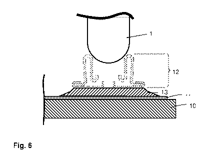
Fig. 6 depicts a cross-section through a pane with the electrical connection
element 12 of
Fig. 5 during the soldering operation according to the invention. The pane is,
for example,
a rear window of an automobile and comprises a substrate 1, which is a 3-mm-
thick
thermally prestressed single-pane safety glass made of soda lime glass. An
electrically
conductive structure 11 in the form of a heated conductor structure is printed
on the
substrate 10. The electrically conductive structure 11 contains silver
particles and glass
frits. In the edge region of the pane, the electrically conductive structure
11 is widened to
a width of approx. 10 mm and forms a contact surface for the electrical
connection element
12. The connection element 12 serves for the electrical contacting of the
electrically
conductive structure 11 to an external voltage supply via a connection cable
(not shown).
CA 03014303 2018-08-10
16
The electrical contacting is hidden from a viewer outside the automobile by a
masking
screen print between the electrically conductive structure 11 and the
substrate 10.
The connection element 12 is to be connected to the electrically conductive
structure 11
via a soldering compound 13. To this end, the soldering compound 13 is
arranged between
the conductive structure 11 and the connection element 12 and fuzed using the
soldering
tip 1. For this, the soldering tip 1 is brought into contact with the
connection element 12,
via which the necessary heat energy is introduced into the soldering compound
13. The
end portion 2 of the soldering tip 1 is partially inserted into the central
depression of the
connection element 12. Since the soldering tip 1 has a larger diameter than
the depression,
the soldering tip 1 is not fully inserted into the depression. Instead, the
edge region of the
end portion 2 of the soldering tip 1 is in contact with the areas of the
connection element
surrounding the depression, in other words, in this case, the upper edge of
the hollow
cylinder forming the snap. Of course, the depression must have a minimum depth
depending on the radius of the end portion of the soldering tip 1 such that
the soldering tip
can be sufficiently lowered to establish the desired contact between the
soldering tip 1 and
connection 12.
From the figure, the advantage of the soldering tip 1 according to the
invention is
immediately obvious. Due to the hemispherical shape of the end portion 2, the
contact
between the soldering tip 1 and the connection element 12 illustrated is
always achieved
independently of the working angle of the soldering tip 1 relative to the
substrate 10. During
hand soldering, the technician thus need not be concerned with maintaining a
precise
working angle and, for example, with always holding the soldering iron exactly
perpendicular to the substrate 10. This significantly facilitates the hand
soldering.
Moreover, the energy is introduced very homogeneously via the circular contact
surface
into the soldering compound 13, for the fuzing of which, consequently, less
energy is
necessary than with point-wise, decentralized energy input. Therefore, the
soldering
compound 13 is less strongly heated overall and solidifies faster after the
end of the
application of energy such that an undesirable shifting of the connection
element 12 on
the still liquid soldering compound 13 can be avoided, even without further
securing
measures. The positioning accuracy of the connection element 12 on the
substrate 10 can
thus be increased; the production tolerances can be reduced. These are major
advantages
of the present invention.
CA 03014303 2018-08-10
17
Fig. 7 depicts a cross-section through a pane with an alternative preferred
embodiment of
the electrical connection element 12 during the soldering operation according
to the
invention. The connection element 12 is implemented as a so-called B crimp ¨
it consists
of a small metal plate with a material thickness of, for example, 0.4 mm, for
example, a
copper plate or a stainless steel plate, that was bent around one end portion
of a
connection cable 14 and was durably stably connected to the connection cable
14 by
crimping. The name "B Crimp" results from the characteristic shape of the
connection
element 12, obtained by plugging the bent-around side edges of the connection
element
12 into the connection cable 14. The characteristic crimp shape shows, in
profile, two
rounded structures (arches) like the letter "B". The connection cable 14 is
implemented as
a stranded wire conductor, whose individual strands are uniformly diverted to
the two sides
of the contact interior, which results in advantageous stability and gas-
tightness of the
crimp contact. The crimp base forms the contact surface for the soldering
compound 13;
whereas, the characteristic crimp structure in the shape of a double arch is
turned away
from the substrate 10. The characteristic crimp structure forms a central
depression into
which the end portion 2 of the soldering tip 1 is partially inserted. The
soldering tip 1 thus
makes contact with the areas on the two arches surrounding the depression.
The depression of the connection element 12 is, in this embodiment, not
peripherally
surrounded by adjacent regions, but, instead, extends over the entire length
of the
connection element 12. The depression is delimited on two sides by the
elevated arches.
The length of the connection element 12 is, for example, 4.5 mm (crimp
length), the width
(crimp width) approx. 2.5 mm, and in the height approx. 1.5 mm (crimp height).
Fig. 8 depicts an exemplary embodiment of the method according to the
invention for
producing a pane with an electrical connection element 12 using the soldering
tip 1
according to the invention.
Examples
Connection elements in the form of snaps (Fig. 5, Fig. 6) were soldered with a
hand-held
soldering iron to a silver print on the glass pane, in one case, using a
soldering tip
according to the invention and, in another, using a conventional soldering
chisel. The
connection elements soldered according to the invention had a stable solder
joint at the
rate of 100%; whereas, the conventionally soldered connection elements did not
hold on
CA 03014303 2018-08-10
18
the silver print (0% stable solder joint). The reason for this resides in the
small contact
area between the conventional chisel form and the snap, as a result of which
low energy
input was effected. The hemispherical soldering tip according to the invention
effected, in
contrast, efficient energy input, as a result of which the soldering compound
is effectively
fuzed and the connection element is stably soldered.
In addition, connection elements in the form of a B crimp (Fig. 7) were
soldered with a
hand-held soldering iron to a silver print on a glass pane, in one case, using
a soldering
tip according to the invention and, in another, using a conventional soldering
chisel. The
connection elements soldered according to the invention had a clean solder
joint at the
rate of 100%. In contrast, with the conventionally soldered connection
elements, in approx.
50% of the cases, uncontrolled outflow of the soldering compound was observed,
as a
result of which the soldering compound sometimes made undesirable contact with
the
conductive core of the connection cable inside the crimp. The reason resides
in the
significantly more homogeneous energy input by the soldering tip according to
the
invention, by means of which the soldering compound is fuzed in a more
controlled
manner.
CA 03014303 2018-08-10
19
List of Reference Characters
(1) soldering tip
(2) end portion of the soldering tip 1
(3) middle portion of the soldering tip 1
(4) connection portion of the soldering tip 1
(5) hand-held soldering iron
(6) union nut
(7) control unit
(8) cable between hand-held soldering iron 5 and control unit 6
(10) substrate
(11) electrically conductive structure
(12) electrical connection element
(13) soldering compound
(14) connection cable of the connection element 12