Note: Descriptions are shown in the official language in which they were submitted.
CA 03015159 2018-08-20
WO 2017/153750
PCT/GB2017/050621
1
METHOD OF REDUCING PHOTOELECTRON YIELD AND/OR SECONDARY ELECTRON
YIELD OF A CERAMIC SURFACE; CORRESPONDING APPARATUS AND PRODUCT
The present invention relates to methods of, and apparatus for, processing
ceramic surfaces
in order to reduce photoelectron yield (PEY) and/or secondary electron yield
(SEY).
BACKGROUND
Photoelectron emission (PEE) refers to the emission of electrons due to
interaction of
photons with a surface. Secondary electron emission (SEE) refers to emission
of a
secondary electron from a surface due to interaction of a primary electron
with the surface.
Photoelectron yield (PEY) can be used to characterise PEE and secondary
electron yield
(SEY) can be used to characterise SEE. PEY and SEY may be taken to be the
average
number of emitted electrons per single incident photon or electron
respectively.
PEE and SEE effects can cause significant difficulties in a wide variety of
apparatus, for
example in particle accelerators, beamlines, waveguides, for example r.f.
waveguides,
detectors, spacecraft, and vacuum chambers. PEE and SEE effects can lead,
variously, to
undesired electron cloud build-up, undesired increases in pressure, beam
losses and
instability, reduction in beam lifetimes, undesired heat loads, power loss,
damage, reduction
in apparatus lifetime, increase in noise, and decrease in sensitivity,
depending on the
particular type of apparatus and application in question.
The reduction of SEY or PEY for ceramic materials, such as > 99.5 % pure
aluminium oxide
(alumina), for example 99.7% pure alumina used for Kickers in accelerator beam
transfer
(Injection Kicker Systems) can be particularly challenging as, for example,
SEY values may
be significantly higher (for example 8 or above) than desired for some
practical applications
(for example less than 2, or less than 1.6 or even 1.4 in some cases).
Although A1203 is
generally referred to as aluminium oxide or alumina, it is also known in the
art to refer to it as
alumina oxide.
It is desired to provide improved or at least alternative methods for reducing
PEY and SEY.
CA 03015159 2018-08-20
WO 2017/153750
PCT/GB2017/050621
2
SUMMARY
In a first aspect of the invention there is provided a method of reducing
photoelectron yield
(PEY) and/or secondary electron yield (SEY) of a ceramic surface, comprising
applying laser
radiation to the surface to produce a periodic arrangement of structures on
the surface.
The laser radiation may comprise pulsed laser radiation comprising a series of
laser pulses.
A ceramic material, for example the ceramic surface, may comprise metallic and
non-
metallic atoms joined by ionic bonds and/or covalent bonds, for example a
mixture of ionic
bonds and covalent bonds.
The power density of the laser radiation, for example of the pulses, may be in
the TW/cm2
range, optionally in a range 0.1 TW/cm2 to 3 TW/cm2. Optionally the power
density may be in
a range 0.5 TW/cm2 to 1.5 TW/cm2.
Alternatively, power density of the laser radiation, for example of the
pulses, may be in the
GW/cm2 range, optionally in a range 0.1 GW/cm2 to 3 GW/cm2. Optionally the
power density
may be in a range 0.2 GW/cm2 to 1 GW/cm2.
By using laser pulses having such power densities in the TW/cm2 range or in
the GW/cm2
range, a periodic arrangement of structures that provides a surface with
desired electron
work function properties may be obtained. For example a surface having a
desired value or
range of values of secondary electron yield (SEY) may be obtained.
The method may alter the properties of surface such that the surface has a
value of SEY
less than 2.5, optionally less than 2.0, optionally less than or equal to 1.6,
optionally less
than or equal to 1.4, optionally in a range 0.2 to 2.0, optionally in a range
0.5 to 1.6,
optionally in a range 1.0 to 1.4.
The laser pulses may have a duration less than a thermal relaxation time of
the material of
the surface. The laser pulses may have a duration such that the electrons and
the atomic
lattice of the material of the surface have a substantially different
temperature substantially
throughout application of the laser pulses. The laser pulses may have a
duration such that
material of the surface is at least one of evaporated or vaporised or removed
without
substantial melting and/or flowing of the surface. The laser pulses may have a
duration such
CA 03015159 2018-08-20
WO 2017/153750
PCT/GB2017/050621
3
that some material of the surface is at least one of evaporated or vaporised
or removed
without substantial melting and/or flowing of the remaining material of the
surface.
A pulse duration of the laser pulses may be in a range 300 femtoseconds (fs)
to 1
nanosecond (ns).
A pulse duration of the laser pulses may be in a range 1 ns to 100 ns.
The periodic arrangement of structures on the surface may comprise a periodic
series of
peaks and troughs substantially parallel to each other, and the peaks may be
substantially
flat on top and/or may be rounded on top and/or may have substantially no
pointed and/or or
sharp regions on top. The peaks may substantially have a top hat shape and/or
a truncated
pyramidal shape, for example a top hat shape and/or a truncated pyramidal
shape in cross-
sectional profile. Thus, for example, a desired value of electron work
function and/or desired
electron trapping properties may be obtained. The peaks may extend in a
longitudinal
direction and may be referred to as ridges.
The peak to trough distance for at least some of the peaks, and/or an average
or median
peak to trough distance, may be in a range 1 m to 100 m, optionally in a
range 20 m to
80 m, optionally in a range 30 m to 60 m.
The periodic arrangement of structures may comprise a cross-hatched
arrangement or an
arrangement of substantially parallel lines of peaks and troughs (for example,
ridges and
valleys) substantially without cross-hatching. The periodic arrangement of
structures may,
for example, be produced by a single pass of a laser source that provided the
laser radiation.
The ceramic surface may be on an at least one underlying layer and the laser
radiation may
be such as to substantially not remove or move material of the surface in such
a way as to
expose the underlying layer.
In a further aspect of the invention, which may be provided independently,
there is provided
a ceramic laser treated surface comprising a laser-formed periodic arrangement
of
structures on the ceramic surface, wherein at least one of:
the periodic arrangement of structures comprises a periodic series of peaks
and
troughs substantially parallel to each other;
CA 03015159 2018-08-20
WO 2017/153750
PCT/GB2017/050621
4
the periodic arrangement of structures comprises a cross-hatched, periodic
series of
peaks and troughs; and optionally
the peaks may be substantially flat on top and/or may be rounded on top and/or
may
have substantially no pointed and/or or sharp regions on top and/or the peaks
may
substantially have a top hat shape and/or a truncated pyramidal shape, for
example a top
hat shape and/or a truncated pyramidal shape in cross-sectional profile;
and/or
the peak to trough distance for at least some of the peaks, and/or an average
or
median peak to trough distance, may be in a range 1 pm to 100 pm, optionally
in a range 20
pm to 80 pm, optionally in a range 30 pm to 60 pm.
In a further aspect of the invention, which may be provided independently,
there is provided
an apparatus for reducing photoelectron yield (PEY) and/or secondary electron
yield (SEY)
of a ceramic surface, comprising:
a laser source for applying pulsed laser radiation to a surface; and
a laser controller configured to control the laser source to apply the laser
radiation as
a series of laser pulses thereby to form a periodic arrangement of structures
on the surface.
The power density of the pulses may be in the TW/cm2 range or in the GW/cm2
range. The
power density of the pulses may be a range 0.1 TW/cm2 to 3 TW/cm2. The power
density of
the pulses may be a range 0.1 GW/cm2 to 3 GW/cm2.
In a further aspect of the invention, there is provided a method of reducing
photoelectron
yield (PEY) and/or secondary electron yield (SEY) of a ceramic surface,
comprising:
applying laser radiation to the surface to produce a periodic arrangement of
structures on the ceramic surface, wherein
the laser radiation comprises pulsed laser radiation comprising a series of
laser
pulses, and a pulse duration of the laser pulses is in a range 300 fs to 1 ns
or in a range 1 ns
to 100 ns.
The surface may be the surface of a target.
The pulse duration may be in a range 1 ps to 100 ps. The pulse duration may be
in a range
1 ps to 50 ps. The pulse duration may be in a range 5ps to 500 ps
The laser radiation may comprise a pulsed laser beam that has a focal spot
diameter on the
surface in a range 5 gm to 100 gm or in a range 1 gm to 100 gm.
CA 03015159 2018-08-20
WO 2017/153750
PCT/GB2017/050621
The pulsed radiation may have a pulse repetition rate in a range 10 kHz to 1
MHz, optionally
in a range 10 KHz to 200 kHz.
5 An average power of the laser radiation may be in a range 3W to 8W or in
a range 1W to
10W. An average power of the laser radiation may be in a range 0.3 W to 2W, or
in a range
1 W to 5W, or in a range 0.1 W to 1 W, or in a range 0.1 W to 2 W, or in a
range 0.3W to
5W.
The applying of the laser radiation to the surface may comprise scanning a
pulsed laser
beam over the surface, and a scan speed for the scanning may be in a range 1
mm/s to 100
mm/s or in a range 10 mm/s to 50 mm/s.
The scanning of the pulsed laser beam over the surface may be repeated between
2 and 10
times, or may be performed once.
An angle of incidence of the laser radiation to the surface may be in a range
from 0 to 30
degrees. The angle of incidence of the laser radiation to the surface may be
in a range from
90 degree to 60 degrees.
A wavelength of the radiation may be in a range 100 nm to 2,000 nm, optionally
355 nm or
532 nm or 1064 nm.
The structures may comprise peaks and troughs. The periodic arrangement of
structures
may comprise a periodic series of peaks and troughs. The peaks and troughs may
be
substantially parallel to each other.
The periodic arrangement of structures may comprise a first series of peaks
and troughs
arranged in a first direction, and a second series of peaks and troughs
arranged in a second,
different direction. The first and second directions may be substantially
orthogonal. The first
series of peaks and troughs and the second series of peaks and troughs may
intersect such
that the periodic arrangement of structures comprises a cross-hatched
arrangement.
A period of the periodic arrangement may be in a range 0.5 j_tm to 100 gm. The
separation
of adjacent peaks (or troughs) of the periodic structure may be in a range 0.5
j_tm to 100 gm.
CA 03015159 2018-08-20
WO 2017/153750
PCT/GB2017/050621
6
A hatch distance of the cross-hatched arrangement may be in a range 0.5 j_tm
to 100 gm,
optionally in a range 10 j_tm to 100 gm.
The laser radiation may be such that the applying of the laser radiation to
the surface
comprises producing further structures. The further structures may be smaller
than the
structures of the periodic arrangement of structures.
That feature may be particularly important, so in a second aspect of the
invention, which
may be provided independently, there is provided a method of reducing
photoelectron yield
(PEY) and/or secondary electron yield (SEY) of a ceramic surface, comprising:
applying laser radiation to the surface to produce a periodic arrangement of
structures on the surface, wherein
the laser radiation comprises pulsed laser radiation comprising a series of
laser
pulses, and the laser radiation is such as to produce further structures on
the surface as well
as the periodic arrangement of structures.
The further structures may comprise further periodic structures. The further
structures may
comprise ripples. The further structures may comprise nano-ripples. The
further structures
may be further periodic structures. The further structures may comprise laser
induced
periodic surface structures (LIPPS), for example with periodicity in the range
of the laser
wavelength. The further structures may have a periodicity in a range 10 nm
to 1 gm,
optionally in a range 100 nm to 1 gm.
The further structures may cover at least part of the periodic array of
structures. The further
structures may be formed in the troughs and/or on the peaks of the periodic
arrangement of
structures.
The ceramic surface and/or target may comprise alumina. For example, > 99.5 %
pure
alumina oxide used for Kickers in accelerator beam transfer (Injection Kicker
Systems).
The ceramic surface and/or target may comprise any suitable magnetic,
conductive or
dielectric ceramic material.
The surface and/or target may comprise a ceramic material having a spinel
structure, for
instance a spinel structure having the formula M(Fe204) where M is a covalent
cation. M
CA 03015159 2018-08-20
WO 2017/153750
PCT/GB2017/050621
7
may be a covalent cation selected from the group manganese (Mn2+), nickel
(Ni2+), cobalt
(002+), zinc (Zn2+), copper (Cu2+), magnesium (Mg2+). Alternatively M may
represent a
monovalent cation, for example lithium (Li) or even a vacancy or vacancies,
for instance in
the case where such absences of positive charge may be compensated for by
additional
trivalent iron cations (Fe3+).
The surface and/or target may comprise a ferrite material, for example a
hexagonal ferrite
material, for instance a material having a structure M(Fe12019). M may be
selected from the
group barium (Ba), strontium (Sr), lead (Pb).
The surface and/or target may comprise a garnet ferrite material, for instance
having the
structure of the silicate mineral garnet, and for example having the chemical
formula
M3(Fe5012) where M may be ytrrium or a rare earth ion.
The surface and/or target may comprise a thick- or thin-film resistor or
electrode or capacitor
or a material that may be suitable for use as or as part of such thick- or
thin-film resistor or
electrode or capacitor. The surface and/or target may comprise a metal oxide
material, for
instance a material selected from the group, lead oxide (Pb0), ruthenium
dioxide (RuO2),
bismuth ruthenate (Bi2Ru207). The surface and/or target may comprise a ceramic
material
having overlapping energy bands.
The surface and/or target may comprise a ceramic conductor. For instance, the
surface
and/or target may comprise indium oxide (In203) and/or tin oxide (Sn02) or
indium tin oxide
(ITO).
The surface and/or target may comprise a heating element or a material that
may be suitable
for use as or as part of such a heating element. The surface and/or target may
comprise
material selected from the group silicon carbide (SiC), molybdenum disilicide
(MoSi2),
lanthanum chromite (LaCr204), zirconia (ZrO2).
The surface and/or target may comprise a thermistor or a material that may be
suitable for
us as or as part of such a thermistor. The surface and/or target may comprise
material
selected from the group consisting of iron spinel material, cobalt spinel
material and
manganese spine! material.
CA 03015159 2018-08-20
WO 2017/153750
PCT/GB2017/050621
8
The surface and/or target may comprise a superconductor material, for example
yttrium
barium copper oxide (YBa2Cu307), a bismuth-strontium-calcium-copper oxide
material (for
example Bi2Sr2Cu06 , Bi2Sr2CaCu208 , or Bi2Sr2Ca2Cu3010), a thallium-barium-
calcium-
copper oxide material (for example TI2Ba2Cu06 , TI2Ba2CaCu208 ,
TI2Ba2Ca2Cu3010, or
TIBa2Ca3Cu4.011) or a mercury-barium-calcium-copper oxide material (for
example
HgBa2Cu04. , HgBa2CaCu206, or HgBa2Ca2Cu308).
The surface and/or target may comprise a perovskite material. The surface
and/or target
may comprise barium titanate (BaTiO3) or barium titanate including non-
stoichiometric lead,
strontium or calcium substitutions.
The surface may form part of a laminated structure, for example a laminated
target, for
instance comprising alumina and at least one other material.
An average or peak fluence or other property of the laser radiation may be
above an ablation
threshold, and/or in the range of thermal threshold of the surface and/or
within 105%,
optionally 102%, optionally 101% of the ablation threshold.
The pulses may be such that, for each pulse, a plasma is formed at the
surface. The plasma
.. may have substantially the same density as underlying material of the
surface.
The surface may form part of a particle accelerator, an injection kicker
system, a beamline, a
waveguide for example an r.f. waveguide, a detector, a detector apparatus, or
a spacecraft.
.. The surface may comprise or form part of a surface of a vacuum chamber.
The surface may comprise a surface of a component of an apparatus. The
apparatus may
be selected from: a particle accelerator, a beam kicker magnet (the component
may for
example comprise a ceramic plate capacitor or ceramic liner pipe), a beamline,
a waveguide
for example an r.f. waveguide, a detector, a detector apparatus, a spacecraft.
The method
may comprise applying the laser radiation to the surface to produce the
periodic
arrangement of structures on the surface and then installing the component in
the apparatus,
or the method may comprise applying the laser radiation to the surface with
the component
in situ in the apparatus.
CA 03015159 2018-08-20
WO 2017/153750
PCT/GB2017/050621
9
The method may comprise applying the radiation using a pulsed solid-state bulk
laser,
optionally the solid state laser comprises a Nd:YV04 or Nd:YAG or Yb:KYW or
Yb:KGW
laser, or a pulsed fibre laser, optionally a Yb, Tm or Nd ¨ doped pulsed solid-
state fibre
laser.
The method may comprise forming a metal layer on at least part of the surface
after the
applying of the laser radiation.
The method may comprise substantially covering the periodic structures with
the metal layer.
The metal layer may be formed using any suitable process, for example a
coating process.
The metal layer may comprise gold or any other suitable metal, for example
silver, copper or
aluminium. The metal layer may comprise elemental metal, for example elemental
gold,
silver, copper or aluminium, or may comprise a metal alloy or metallic
compound.
The metal layer may have a thickness in a range 0.1 nm to 100 nm, optionally 1
nm to 50
nm, optionally 1 nm to 20 nm. The metal layer may have a substantially
constant thickness.
The metal layer may have a thickness such as to maintain the morphology of the
surface, for
example to maintain the surface to have substantially the same cross-sectional
profile as
before the formation of the metal layer. For instance the metal layer may have
a thickness
such as to maintain substantially the same distribution of laser-formed
troughs and peaks at
the surface as before the formation of the metal layer, and/or such as to not
completely fill in
gaps between surface features, for example the troughs and/or peaks or other
laser-formed
surface features.
The method may comprise at least one of degreasing, cleaning or smoothing the
surface
after the applying of the laser radiation and/or performing a surface carbon
reduction
process with respect to said surface after the applying of the laser
radiation.
In a further aspect of the invention, which may be provided independently,
there is provided
an apparatus for reducing photoelectron yield (PEY) and/or secondary electron
yield (SEY)
of a surface, comprising:
a laser source for applying pulsed laser radiation to a surface; and
CA 03015159 2018-08-20
WO 2017/153750
PCT/GB2017/050621
a laser controller configured to control the laser source to apply the laser
radiation as
a series of laser pulses having a pulse duration in a range 200 femtoseconds
(fs) to 1000 ps,
so as to produce a periodic arrangement of structures on the surface.
5 In a further aspect of the invention, which may be provided
independently, there is provided
an apparatus for reducing photoelectron yield (PEY) and/or secondary electron
yield (SEY)
of a ceramic surface, comprising:
a laser source for applying pulsed laser radiation to a surface and configured
to
operate so as to perform a method according to any other aspect.
In a further aspect of the invention, which may be provided independently
there is provided a
laser treated ceramic surface comprising a periodic arrangement of structures
on the surface
formed using a method according to any other aspect.
The surface may further comprise a metal layer covering at least part,
optionally
substantially all, of the periodic arrangement of structures and/or of the
surface. Thus, at
least part optionally all of the outer part of the ceramic surface may
comprise metal.
In a further aspect of the invention, which may be provided independently,
there is provided
a laser treated ceramic surface comprising a laser-formed periodic arrangement
of
structures on the ceramic surface and further laser-formed structures on the
ceramic
surface.
The further structures may comprise further periodic structures. The further
structures may
comprise ripples. The further structures may comprise nano-ripples. The
further structures
may be further periodic structures. The further structures may comprise laser
induced
periodic surface structures (LIPPS). The further structures may have a
periodicity in a range
10 nm to 1 gm, optionally in a range 100 nm to 1 gm.
The structures may comprise peaks and troughs. The periodic arrangement of
structures
may comprise a periodic series of peaks and troughs. The peaks and troughs may
be
substantially parallel to each other.
The periodic arrangement of structures may comprise a first series of peaks
and troughs
arranged in a first direction, and a second series of peaks and troughs
arranged in a second,
CA 03015159 2018-08-20
WO 2017/153750
PCT/GB2017/050621
11
different direction. The first and second directions may be substantially
orthogonal. The first
series of peaks and troughs and the second series of peaks and troughs may
intersect such
that the periodic arrangement of structures comprises a cross-hatched
arrangement.
A period of the periodic arrangement may be in a range 0.5 gm to 100 gm. The
separation
of adjacent peaks (or troughs) of the periodic structure may be in a range 0.5
gm to 100 gm.
A hatch distance of the cross-hatched arrangement may be in a range 0.5 gm to
100 gm.
The further structures may comprise further periodic structures. The further
structures may
comprise ripples. The further structures may comprise nano-ripples. The
further structures
may be further periodic structures. The further structures may comprise laser
induced
periodic surface structures (LIPPS). The
further structures may have a periodicity in a
range 10 nm to 1 gm, optionally in a range 100 nm to 1 gm.
The further structures may cover at least part of the periodic array of
structures. The further
structures may be formed in the troughs of the periodic arrangement of
structures.
The surface may comprise alumina. The surface may form part of a laminated
structure, for
example a laminated target, for instance comprising alumina or other ceramic
and at least
one other material.
In a further aspect of the invention, which may be provided independently,
there is provided
a method of modifying a ceramic surface by applying laser radiation to the
surface to modify
the surface by way of a photo-thermal interaction and/or a photo-ablation
interaction.
In another aspect of the invention, which may be provided independently, there
is provided a
ceramic surface modified by way of a photo-thermal interaction and/or a photo-
ablation
interaction obtained by applying laser radiation to the surface.
In a further aspect of the invention, which may be provided independently,
there is provided
a particle accelerator, an injection kicker system, a beam kicker magnet, a
beamline, a
waveguide, a detector, a spacecraft, or a vacuum chamber that includes a
component
having a ceramic surface according to any of the other aspects or formed
according to any
of the other aspects.
CA 03015159 2018-08-20
WO 2017/153750
PCT/GB2017/050621
12
In further aspects of the invention there are provided a method, a surface, a
structure
comprising a surface, an apparatus, a component, a particle accelerator, an
injection kicker
system, a beam kicker magnet, a beamline, a waveguide, a detector, a
spacecraft, or a
vacuum chamber as described and/or illustrated herein.
Any feature in any one or more of the aspects of the invention may be applied
to any other
one or more of the aspects of the invention in any appropriate combination.
BRIEF DESCRIPTION OF THE DRAWINGS
Embodiments of the invention are further described hereinafter with reference
to the
accompanying drawings, in which:
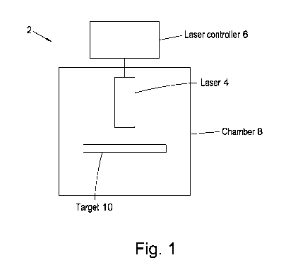
Figure 1 is a schematic diagram of a system used for laser treatment of a
surface to
reduce photoelectron emission (PEE) and/or secondary electron emission (SEE)
effects, for
example to reduce photoelectron yield (PEY) and/or secondary photoelectron
yield (SEY);
Figure 2 is a plot of SEY as a function of primary electron energy for a
sample
according to an embodiment;
Figure 3 is a plot of SEY as a function of primary electron energy for the
reverse side
of the sample of Figure 2;
Figures 4 to 9 are plot of SEY as a function of primary electron energy for
samples
according to further embodiments;
Figures 10a to 10c are scanning electron microscope (SEM) images of surfaces
of
samples according to embodiments;
Figures 11a to 11j are SEM images of surfaces of samples according to further
embodiments;
Figure 12 is a graph showing total reflectance, total transmittance and
absorptance
for samples;
Figure 13 is a plot of SEY as a function of primary electron energy for a
sample
according to a further embodiment;
Figure 14 is a plot of SEY as a function of primary electron energy for the
sample of
Figure 13, including data after conditioning and exposure to air of the
sample;
Figures 15a and 15b are SEM images of surfaces of samples according to
embodiments;
Figures 16a to 16n are SEM images of surfaces of samples according to further
embodiments;
CA 03015159 2018-08-20
WO 2017/153750
PCT/GB2017/050621
13
Figures 17a and 17b are schematic illustrations of photo-thermal interaction
(PTI)
and photo-ablation interaction (PAI) mechanisms;
Figure 18 is a plot of measurements SEY as a function of primary energy for
alumina
ceramic samples, both before and after coating with a layer of gold; and
Figures 19 and 20 are SEM images of the surfaces of the samples that are the
subject of Figure 18.
DETAILED DESCRIPTION
Figure 1 shows a system used for laser treatment of a surface to reduce
photoelectron
emission (PEE) and/or secondary electron emission (SEE) effects, for example
to reduce
photoelectron yield (PEY) and/or secondary electron yield (SEY).
The system 2 of Figure 1 comprises a laser 4 connected to a laser controller 6
which is used
to control operation of the laser 4 to emit a pulsed laser radiation beam of
desired
characteristics. The laser 4 is aligned with a target 8 such that operation of
the laser 4 under
control of the laser controller 6 forms periodic structures on the surface of
the target.
In embodiments, the laser may be one of a pulsed Nd:YV04 or Nd:YAG or Yb:KYW
or
Yb:KGW solid-state bulk laser, or a pulsed fibre laser, optionally a Yb, Tm or
Nd ¨ doped
pulsed solid-state fibre laser. Any
other suitable laser may be used in alternative
embodiments. In the embodiment of Figure 1, the wavelength of the pulsed laser
radiation is
532 nm, but any other suitable wavelength can be used in other embodiments,
for example
1064 nm or 355 nm.
The controller may comprise a dedicated controller, or a suitably programmed
computer.
The controller may be implemented in software, hardware or any suitable
combination of
hardware and software. In some embodiments, the controller may comprise more
ASICs
(application specific integrated circuits) or FPGAs (field programmable gate
arrays) or other
suitable circuitry.
In the embodiment of Figure 1, the target 8 and laser 4 are located in air and
the laser
treatment of the surface is performed in air. The target 8 and laser 4 may be
positioned in a
sealable and/or pumpable chamber 10 that has an associated pump and/or gas
supply, and
the laser processing of the surface may be performed in vacuum or in desired
gaseous
CA 03015159 2018-08-20
WO 2017/153750
PCT/GB2017/050621
14
conditions, for example in the presence of a selected reactive gas or inert
gas. The chamber
is omitted in some embodiments.
In the embodiment of Figure 1, the target is a ceramic target comprising
alumina, for
5 example 99.5% or greater than 99.5% pure alumina. Other ceramic targets
may be used in
other embodiments. For instance, the target may comprise any suitable
magnetic,
conductive or dielectric ceramic material.
For instance, the target may comprise a ceramic material having a spinel
structure, for
10 instance a spinel structure having the formula M(Fe204) where M is a
covalent cation. M
may be a covalent cation selected from the group manganese (Mn2+), nickel
(Ni2+), cobalt
(002+), zinc (Zn2+), copper (Cu2+), magnesium (Mg2+). Alternatively M may
represent a
monovalent cation, for example lithium (Li) or even a vacancy or vacancies,
for instance in
the case where such absences of positive charge may be compensated for by
additional
trivalent iron cations (Fe3+).
Alternatively, in some embodiments the ceramic target may comprise a ferrite
material, for
example a hexagonal ferrite material, for instance a material having a
structure M(Fe12019).
M may be selected from the group barium (Ba), strontium (Sr), lead (Pb).
In other embodiments, the ceramic target may comprise a garnet ferrite
material, for
instance having the structure of the silicate mineral garnet, and for example
having the
chemical formula M3(Fe5012) where M may be ytrrium or a rare earth ion.
In some embodiments, the ceramic target may comprise a thick- or thin-film
resistor or
electrode or a material that may be suitable for use as or as part of such
thick- or thin-film
resistor or electrode. In embodiments, the ceramic target may comprise a metal
oxide
material, for instance a material selected from the group, lead oxide (Pb0),
ruthenium
dioxide (RuO2), bismuth ruthenate (Bi2Ru207). The ceramic target may comprise
a ceramic
material having overlapping energy bands.
In other embodiments, the target may comprise a ceramic conductor. For
instance, the
target may comprise indium oxide (In203) and/or tin oxide (Sn02) or indium tin
oxide (ITO).
CA 03015159 2018-08-20
WO 2017/153750
PCT/GB2017/050621
In embodiments, the ceramic target may comprise a heating element or a
material that may
be suitable for use as or as part of such a heating element. In embodiments,
the target may
comprise material selected from the group silicon carbide (SiC), molybdenum
disilicide
(MoSi2), lanthanum chromite (LaCr204), zirconia (ZrO2).
5
In embodiments, the ceramic target may comprise a thermistor or a material
that may be
suitable for us as or as part of such a thermistor. In embodiments, the target
may comprise
material selected from the group consisting of iron spinel material, cobalt
spinel material and
manganese spine! material.
IA)
In embodiments, the ceramic target may comprise a superconductor material, for
example
yttrium barium copper oxide (YBa2Cu307), a bismuth-strontium-calcium-copper
oxide
material (for example Bi2Sr2Cu06 , Bi2Sr2CaCu208 , or Bi2Sr2Ca2Cu3010), a
thallium-barium-
calcium-copper oxide material (for example TI2Ba2Cu06 , TI2Ba2CaCu208 ,
TI2Ba2Ca2Cu3010,
15 or TIBa2Ca3Cu4011) or a mercury-barium-calcium-copper oxide material
(for example
HgBa2Cu04., HgBa2CaCu206, or HgBa2Ca2Cu308).
In embodiments, the target may comprise a perovskite material. In embodiments
the target
may comprise barium titanate (BaTiO3) or barium titanate including non-
stoichiometric lead,
strontium or calcium substitutions.
In operation pulsed laser radiation of desired characteristics is scanned
across the surface of
the target 8 by the laser 4 under control of the laser controller 6 to produce
a periodic
arrangement of structures on the surface. For example, in order to form peaks
and troughs
arranged in parallel rows, the laser beam may be scanned along parallel,
spaced-apart
paths across the surface to form parallel troughs separated by peaks. Any
other suitable
arrangements of structures can be formed by suitable scanning of the laser
beam over the
surface.
Operating parameters of the laser, and certain equations linking such
parameters, can be
represented as follows,
Wavelength (A) [m]
Repetition rate of the laser (y) [Hz]
CA 03015159 2018-08-20
WO 2017/153750
PCT/GB2017/050621
16
Pulse length of the laser (r) [s]
Average power of the laser (Pavg) [W] - represents the energy flow over one
period t
Energy per pulse (Ep) [J]
Fluence of the laser (F) [J/cm2]
Beam spot radius on the target (r) [m]
Beam spot area on the target (A=Trr2)[m2]
Number of times surface of the target was scanned by the laser beam (N)
dimensionless
Speed at which surface of the target was scanned by the laser beam (V) [m/s]
Number of pulses fired per each spot on the surface of the target (n)
[dimensionless]
.. Time interval between the pulses - one period (t) [s]
Peak Power (Ppeak) [W] - defines the energy flow within a single pulse
Power density or Intensity (I) [W/cm2]
Key eauations
t= -1
(2r)y
n= -
V
Pavg
E = -
E Ise
F = 13'='
A
Epulse
Ppeak = ______
= Ppeak
1 -
A
CA 03015159 2018-08-20
WO 2017/153750 PCT/GB2017/050621
17
Suitable operating parameters can be selected, for example based on the
equations and
representations above, to obtain pulsed laser radiation of desired properties,
for example a
desired power density of the pulses.
Table 1 provides operating parameters of the laser of the apparatus of Figure
1 to produce a
desired periodic arrangement of structures on the surface of various samples
of alumina.
The laser processing of the surface was performed in an argon atmosphere for
the PSCA
sample and in air for all of the other samples of Table 1.
PS1 C1 R
Sample name PSCA PS2L1 R PS2C1 R PS2L2R PS2C2R PS4L1 R
Wavelength 532 532 532 532 532 532 532
(nm)
T 10 ps 10 ps 10 ps 10 ps 10 ps 10 ps 10
ps
Repetition rate 200 200
200 200 200 200 200
(kHz)
Power (W) 2 2 2 2 2 4 1
Laser focal spot 12 12 12 12 12 12 12
diameter (pm)
Pulse energy ( 10.00 10.00 10.00 10.00 10.00 20.00 5.00
J)
Fluence (J/cm2) 8.84 8.84 8.84 8.84 8.84 17.68 4.42
Structure Cross lines cross lines cross lines cross
(cross/line)
Hatch distance 24 24 24 24 24 24 24
(1-1m)
Scan speed 6 6 6 6 6 6 6
(m m/s)
Passes 1 1 1 2 2 1 1
Pulses per spot 400 400 400 400 400 400 400
per pass
Width of laser- 14 15.2 15.2 15.2 15.2 15.2 15.2
processed area
CA 03015159 2018-08-20
WO 2017/153750 PCT/GB2017/050621
18
(mm)
Length of laser- 14 15.2 15.2 15.2 15.2 15.2 15.2
processed area
(mm)
Process time 45.37 26.74 53.48 53.48 106.96 26.74
53.48
(minutes)
Table 1
The samples of Table 1 had a thickness of 3 mm, and the laser processed areas
of the
samples were 14 mm by 14 mm (for sample PSCA) or 15.2 mm by 15.2 mm (for the
other
samples). Each of the samples were aluminium oxide (alumina) of greater than
99.7%
purity, which is the grade used for certain particle accelerator applications.
The secondary electron yield (SEY) of each of the samples of Table 1 was
measured for
different primary electron energies at either three or four different spots on
the samples. To
avoid charging effects the surfaces were bombarded with low energy electrons
(36eV)
between each measurement point. The maximum applied dose to measure one data
point
was about 1 x 10-12 C. The total dose to measure one spectrum was therefore
about 1 x 10-
110.
Figure 2 is a plot of SEY as a function of primary electron energy for sample
PSCA at three
different spots on the laser treated surface. Figure 3 is a plot of SEY as a
function of primary
electron energy for sample PSCA at three different spots on the reverse side
of the sample
which was not laser treated, for comparison purposes.
It can be seen that the laser treatment of the surface of the PSCA sample
resulted in a
reduction of SEY from around 8 to 9 (for the untreated reverse surface) to
around 2.2 for the
laser treated surface.
Figures 4 to 9 are plot of SEY as a function of primary electron energy for
samples PS1C1R,
PS2C1R, PS2C2R, PS2L1R, PS2L2R and PS4L1R respectively.
The approximate maximum SEY values for the various samples of Table 1 are
summarised
in Table 2 below.
CA 03015159 2018-08-20
WO 2017/153750
PCT/GB2017/050621
19
Sample Maximum SEY value obtained for laser-
treated surface
PSCA 2.2
PS1C1R 2.2
PS2C1R 1.6
PS2C2R 1.7 (outlier 1.9)
PS2L1R 1.9
PS2L2R 2.2
PS4L1R 2.5
Table 2
Scanning electron microscope (SEM) images of the samples of Table 1 were
obtained, and
show structures formed by the laser treatment of the surfaces of the samples.
Figure 10a is an SEM image of the laser treated surface of sample PSCA.
10b shows SEM images of the laser treated surfaces of the PS2L1R sample (top
left image),
the PS2L2R sample (bottom left image), the PS2C1R sample (top right image) and
the
PS2C2R sample (bottom right image).
Figure 10c shows SEM images of the laser treated surfaces of the PS4L1R sample
(left
hand image) and the PS1C1R sample (right hand image).
Figures lla to 11e are SEM images of laser treated surfaces for which the
power density of
the laser beam was 0.74 TW/cm2, 0.88 TW/cm2, 0.95 TW/cm2, 2 TW/cm2, 1.3 TW/cm2
respectively and the sample was laser treated in an argon atmosphere. Figures
11f to 11j
are SEM images of laser treated surfaces for which the power density of the
laser beam
was 0.3 TW/cm2, 0.4 TW/cm2, 2 TW/cm2, 0.6 TW/cm2 and 1 TW/cm2 respectively and
the
sample was laser treated in air. Other operating parameters were substantially
the same as
for sample PSCA of Table 1.
It is noted that in a normal, unmagnified view of sample PSCA (which was
processed under
argon atmosphere) the surface appeared black, whilst in normal unmagnified
views of the
other samples of Table 1 the surfaces of the samples appeared white, or at
least much
lighter than the surface of sample PSCA.
CA 03015159 2018-08-20
WO 2017/153750
PCT/GB2017/050621
Measurements of the spectral properties of samples of aluminium oxide were
also
performed. Figure 12 is a graph showing total reflectance, total
transmittance and
absorptance of a sample of aluminium oxide (referred to as C Cera, having a
purity of
5 around 99.7%) used by CERN in a kicker magnet and of another sample of
aluminium oxide
(referred to as White Cera) before any laser processing. The spectra show some
absorptance at 532 nm and very low absorptance at 1064 nm. Reflectance is
different for
the samples, which is in accordance with the different colours of the samples
that are
apparent to the human eye. The thickness of both samples was 3 mm. It was
determined
10 from these measurements that laser processing at 532 nm, or 515 nm -
another available
laser wavelength, may be suitable.
It can be seen from the results outlined above that the maximum SEY value
measured for
the laser treated surfaces of the samples of Table 1 varies between 1.6 and
2.2. The
15 sample with the lowest SEY is PS2C1R with a maximum value of 1.6. There
seems to be
substantially no link between reflectivity and the SEY of the samples. Some
samples have
outliers at 200eV electron energy, which could be due to inhomogeneities at
the surface.
In some other embodiments where the sample is alumina, operating parameters
may be
20 selected from Table 3 as follows to produce a desired periodic
arrangement of structures on
the surface of the sample. The values of the operating parameters may also be
selected
from Table 3 in the case of other ceramic materials of interest.
Wavelengt Puls Focal Repetitio Averag Scan Repetitio Hatch Power
h (nm) e spot n rate e speed n distanc density
width diamete (KHz) power (mm/s number e (intensity)
rang r (W) ) (mcm)
e
355 nm, 500f ipm - 10kHz ¨ 1-10 1-100 1-10 10-100 0.1TW/c
532 nm or s ¨ 100 m 200 kHz m2 to
1064 nm ins 3TW/cm 2
Table 3
Good results may be achieved with a power density range of 0.1TW/cm2 to
3TVV/cm2, with
particularly good results for wavelength of 532 nm in the power density range
0.5 TVV/cm2 to
1.5 TW/cm2 for processing in argon. However, highly organised structuring is
achieved for
laser processing in either air or argon.
CA 03015159 2018-08-20
WO 2017/153750
PCT/GB2017/050621
21
The results discussed above in relation to Tables 1 to 3 and Figures 2 to 12
were obtained
using laser beam power densities in the TVV/cm2 range. In alternative
embodiments, laser
patterning of ceramic surfaces is obtained using laser beam power densities in
the GW/cm2
range.
Table 4 provides operating parameters of the laser of the apparatus of Figure
1 to produce a
desired periodic arrangement of structures on the surface of a sample
(referred to as the
NSCA sample) of alumina, using laser beam power densities in the GW/cm2 range.
The
laser processing of the surface was performed in an argon atmosphere for the
NSCA
sample.
Sample name NSCA
Wavelength 532
(nm)
T 10 ns
Repetition rate 20
(kHz)
Power (W) 3.46
Laser focal spot 60
diameter (pm)
Pulse energy ( 173.0
J)
Fluence (J/cm2) 6.12
Structure cross
(cross/line)
Hatch distance 70
Ulm)
Scan speed 20
(m m/s)
Passes 10
Pulses per spot 60
per pass
Width of laser- 14
processed area
(mm)
Length of laser- 14
processed area
(mm)
Process time 46.67
(minutes)
Table 4
CA 03015159 2018-08-20
WO 2017/153750
PCT/GB2017/050621
22
Table 4 is in the same format as Table 1 above, which provided operating
parameters for
certain samples treated with laser power densities in the TW/cm2 range.
The NSCA sample of Table 1 had a thickness of 3 mm, and the laser processed
area of the
samples was 14 mm by 14 mm. The sample was aluminium oxide (alumina) of
greater than
99.7% purity, which is the grade used for certain particle accelerator
applications.
The secondary electron yield (SEY) of the NSCA sample of Table 4 was measured
for
different primary electron energies at three different spots on the sample. To
avoid charging
effects the surfaces were bombarded with low energy electrons (36eV) between
each
measurement point. The maximum applied dose to measure one data point was
about 1 x
10-12 C. The total dose to measure one spectrum was therefore about 1 x 10-
11C.
Figure 13 is a plot of SEY as a function of primary electron energy for sample
NSCA at three
different spots on the laser treated surface.
After the performance of the SEY measurements, the NSCA sample was conditioned
in an
attempt to obtain even lower SEY values by bombarding the sample with 500eV
electrons up
to a total dose of 1 x 10⁻² C/mm2 and then exposing the sample to air during
one night.
Figure 14 is a plot of SEY as a function of primary electron energy for sample
NSCA at three
different spots on the laser treated surface following the conditioning using
500eV electrons
and exposure to air. The SEY results of Figure 13 are also included on Figure
14 for
comparison.
It was found that the SEY results of Figure 14 obtained after the conditioning
and air
exposure showed an increased maximum SEY, suggesting a reactive surface. The
measurements of SEY spectra after the conditioning and air exposure were not
well
reproducible, for which a possible reason may be implantation of charges into
the bulk of the
ceramic.
To verify the charging of the NSCA sample surface, X-ray photoelectron
spectroscopy
measurements to obtain an XPS spectrum were performed following the
conditioning and air
exposure. The XPS spectrum indicated that aluminium (15 atomic %) and oxygen
(79
CA 03015159 2018-08-20
WO 2017/153750
PCT/GB2017/050621
23
atomic %) were the main elements present, that carbon contamination was low (1
atomic %)
and that some fluorine was present (5 atomic %).
Figures 15a and 15b are SEM images, at different levels of magnification, of
the laser
treated surface of sample NSCA.
Figures 16a to 16d are SEM images of laser treated surfaces for which the
power density of
the laser beam was 0.25 GW/cm2, 0.35 GW/cm2, 0.45 GW/cm2, and 0.55 GW/cm2
respectively and the sample was laser treated in air. Figures 16e to 16n are
SEM images of
laser treated surfaces for which the power density of the laser beam was 0.6
GW/cm2, 0.65
GW/cm2, 0.7 GW/cm2, 0.75 GW/cm2, 0.8 GW/cm2, 0.85 GW/cm2, 0.9 GW/cm2, 0.95
GW/cm2, 1 GW/cm2 and 1.5 GW/cm2 respectively and the sample was laser treated
in an
argon atmosphere. Other operating parameters were substantially the same as
for sample
NSCA of Table 4.
In some other embodiments where the sample is alumina, operating parameters
may be
selected from Table 5 as follows to produce a desired periodic arrangement of
structures on
the surface of the sample. The values of the operating parameters may also be
selected
from Table 5 in the case of other ceramic materials of interest.
Waveleng Puls Focal Repetitio Averag Scan Repetitio Hatch Power
th (nm) e spot n rate e speed n distanc density
width diamet (KHz) power (mm/ number e (intensity)
rang er (W) s) (mcm)
e
355 nm, ins 20 m - 10kHz ¨ 3-8 10-50 1-10 10-100 0.002GW/c
532 nm or ¨ 100 m 200 kHz m2 to
1064 nm 100n 3GW/cm2
s
Table 5
Good results may be achieved with a power density range of 0.1GW/cm2 to
3GW/cm2, with
particularly good results for wavelength of 532 nm in the power density range
0.2 GW/cm2 to
1 GW/cm2 for processing in argon. However, highly organised structuring is
achieved for
laser processing in either air or argon.
It is a feature of embodiments that periodic structures can be formed on
ceramic surfaces by
applying to the surfaces laser radiation having a power density in the TW/cm2
range or in the
CA 03015159 2018-08-20
WO 2017/153750
PCT/GB2017/050621
24
GW/cm2 range. Without wishing to be bound by theory, and without limitation to
the scope
of protection, the following comments are provided which relate to processes
which may
occur in relation to at least some embodiments.
Laser engineering provides an overarching methodology that provides for the
formation of
periodic structures according to embodiments. Precision laser engineering is
expected to
excite free electrons within metals, vibrations within insulators, and indeed
both types of
excitations within semiconductors. The mechanisms by which lasers can engineer
materials
include the following:
(i) Photo-thermal interaction (PTI) ¨ commonly achieved using laser beams
providing
short dwell time (e.g. lasers with nanosecond pulsewidth);
(ii) Photo-ablation interaction (PAI) ¨ envisaged using laser beams
providing ultra-short
dwell time (e.g. lasers with picosecond or femtosecond pulsewidth).
The laser processing in respect of the embodiments described in relation to
Tables 4 and 5
and Figures 13 to 16 may be in the PTI regime. The laser processing in respect
of the
embodiments described in relation to Tables 1 to 3 and Figures 2 to 11 may be
in the PAI
regime.
In the PTI regime the focused laser beam acts as a spatially confined, intense
heat source.
Targeted material is heated up rapidly, eventually causing it to be vaporized.
Without
wishing to imply any limitation to the scope of protection, the targeted
material could be
referred to as being boiled away. An advantage of this approach is that it may
enable rapid
removal of relatively large amount of target material. However, the peripheral
heat affected
zone (HAZ) damage and the presence of some recast material after processing
present
limitations in terms of heat confinement for precision laser materials
engineering.
In the PAI regime, the laser drives multi-photon absorption of light inside
the material. This
strips electrons from the material, which then explode away due to Coulomb
repulsion.
Because PAI involves directly breaking the molecular or atomic bonds that hold
the material
together, rather than simply heating it, it is intrinsically not a 'hot'
process. Since the material
is removed in a very short timeframe, the ablated material carries away most
of the energy
before heat can spread into the surrounding material. These effects may result
in a
significantly reduced HAZ. Furthermore, this is a clean process and may leave
minimal
CA 03015159 2018-08-20
WO 2017/153750
PCT/GB2017/050621
recast material, thereby eliminating the need for elaborate post-processing.
The PAI
mechanism is compatible with a very broad range of materials, including high
band-gap
materials that have low linear optical absorption and therefore are difficult
to engineer with
existing techniques. The PAI mechanism can be considered 'wavelength neutral';
that is,
5 nonlinear absorption can be reduced even if the material is normally
transmissive at the
laser wavelength.
The PAI mechanism should fundamentally allow for custom design of electron
work function
of ceramic surfaces. Ceramics usually consist of metallic and non-metallic
atoms joined by
10 bonds that are partly ionic and partly covalent, giving them such
properties such as
hardness, brittleness and resistance to heat. Therefore, it may be of
importance to correctly
identify parameters that may play a significant role in the light-matter
interaction mechanisms
in these materials and ultimately contribute to challenges of the laser
precision structuring
processes and the design of the surface potential of ceramic surfaces.
The PTI and PAI mechanism are illustrated schematically in Figures 17a and 17b
respectively.
It is a further feature of embodiments that the characteristics of the pulsed
radiation that is
applied to the surface, for example the use of pulse durations in the
picosecond range or
less, may be such that the periodic structures that are formed may be of
shallower depth
and/or more gently sloped than features formed using pulsed radiation of
higher energy
and/or longer duration for example pulse durations in the nano-second range.
Again without wishing to be bound by theory, and without limitation to the
scope of
protection, the following further comments are provided which relate to
processes which may
occur in relation to at least some embodiments.
In irradiation at very high intensities (or high irradiance) one is confronted
with the issue of a
dense, strongly absorbing material, in the first few tens of nm of which
energy at a rate of
some 1020 W/cm3 is liberated. Part of this energy, once randomised, is
conducted into the
bulk of the material, while part is converted into directed kinetic energy by
thermal expansion
of the heated layer. Two regimes are distinguished in this respect.
CA 03015159 2018-08-20
WO 2017/153750
PCT/GB2017/050621
26
1. Nanosecond pulsed laser interaction which is dominated by the expansion and
ablation of
material. Here the thermal pressure of the heated layer is sufficient to cause
significant
compression of the underlying target material.
2. Picosecond pulsed laser interaction (which is heat conduction dominated
since
hydrodynamic motion during the pulse duration is negligible (laser pulses here
may be 1000
times or more shorter than nanosecond ones). In the picosecond regime the
strong heating
of the dense material may occur before hydrodynamic expansion of the processed
layer has
even started. The plasmas produced in this regime may have essentially the
same density
as the solid target itself. This - upon cooling - leads to the formation of
fine structures - in the
range from 1 micrometres to 50 micrometres depending on the irradiation
parameters -
covered with nano-structures.
Using picosecond duration pulsed radiation according to some embodiments can
in some
cases also cause formation of nano-ripples or other small scale structures on
the surface in
addition to the larger scale peaks and troughs obtained by scanning the laser
beam in an
appropriate pattern over the surface. It is possible that such nano-ripples or
other small
scale structures may in some cases decrease the PEY or SEY further, in
addition to the
reduction obtained by larger periodic peak and trough structures. Furthermore,
in some
cases the nano-ripples or other small scale structures and/or the shallower
peaks and
troughs associate with picosecond rather than nanosecond pulses may also
provide
improved or alternative electrical properties of the surface, for example
reduced induction,
and/or can provide the surface with an increased area at the nano- or micro-
scale.
Again, without wishing to be bound by theory, and without limitation to the
scope of
protection, further comments are as follows.
With increasing surface roughness the maximum SEY may decrease for a surface
characterized by (for example statistically containing) more valleys, while it
may increase
significantly at a surface spread with (for example statistically containing)
more hills. The
observation indicates that hill and valley structures may be very effective in
increasing and
decreasing the SEY, respectively, due to their different morphologic features
and surface
electron work functions (EWF).
CA 03015159 2018-08-20
WO 2017/153750
PCT/GB2017/050621
27
The total SEY may denote the ratio of both emitted true secondary electrons
(SEs) and
backscattered electrons (BSEs) to primary electrons (PEs) incident to the
surface.
Example: Sample surfaces exposed to air can be easily contaminated by adsorbed
gases
and hydrocarbons, and their SEY may increase.
High SEY caused by contaminations should be likely to give rise to the
electron
multiplication and eventually degrades the performance of microwave devices
and the
destructive electron-cloud instability in large particle accelerators.
Increase in SEY indicates the reduction in electron work function (EWF).
With increasing roughness SEYrnax has a significant increase for surfaces that
are spared by
hills. This phenomenon implies that hill structures should play a positive
role in the SE
emission. Moreover, SEY,õax decreases rapidly by surfaces that are mainly
characterized by
valleys, which should be the dominant factor of the reduction in
SEYmax=
In the case of valley structures, SEs can be trapped effectively through
collisions with
sidewalls, thus the SEY declines. Nevertheless, for hill structures, apart
from the negative
effect of sidewalls, there are some positive effects on SE emission. For
example, some PEs
strike the local surfaces with hills obliquely, which will induce more SEs
than normal
incidence. Additionally, SEs are likely to re-enter sidewalls of the hills,
resulting in further
SEs generations. Most re-entered SEs should be the BSEs those with high
energies to
overcome the surface potential barrier and generate plenty of true SEs with
low energies
escaping to the vacuum.
Changes in the electron work function (EWF) induced by different surface
morphologies may
also be responsible for the SEY variations. The work function may decrease at
surface
peaks and increases at surface valleys with increasing the surface roughness.
Hills and
valleys in our structuring work may be considered as surface peaks and
valleys. A rougher
surface introduced by hill structures often has a lower electron work function
(EWF), thus the
SEY naturally increases. However, the EWF will be enhanced by roughing a
surface with
valley structures, and finally the SEY decreases.
CA 03015159 2018-08-20
WO 2017/153750
PCT/GB2017/050621
28
It has been found that forming of a metal layer on the ceramic surface after
the laser
treatment that forms the periodic structures can result in a significant
reduction of SEY.
Figure 18 is a plot of measurements SEY as a function of primary energy for
the alumina
ceramic samples with sample names PS2C1R and PS2C1R mentioned above, both
before
and after coating with a layer of gold of 10 nm thickness. It can be seen that
there is a
significant reduction of SEY for both samples.
Figures 19 and 20 show SEM images of the surfaces of the PS2C1R and PS2C1R
alumina
sample after coating with the gold layer.
In alternative embodiments any other suitable metal of any other suitable
thickness may be
used for the metal layer on the ceramic surface.
The layer of gold or other metal may be formed using any suitable deposition
process, for
example any suitable chemical or physical vapour deposition process, for
instance a
sputtering process, an evaporative deposition process or a laser deposition
process. By way
of example, an Edwards (RTM) 308 coating unit may be used to form the coating.
Any other
suitable deposition apparatus may be used.
In alternative embodiments, the ceramic surface, or a metal layer deposited on
the ceramic
surface may be subject to a degreasing, cleaning or smoothing process and/or a
surface
carbon reduction process after the applying of the laser radiation, which may
result in a
decrease in SEY. Cleaning using an NGL (RTM) degreasing product may be used.
Any
suitable degreasing, cleaning, smoothing or surface carbon reduction process
may be used
in alternative embodiments. The degreaser may, in some embodiments, be such as
to not
change substantially the morphology of the sample but may remove a layer of
carbon or
carbon-containing compounds, mixtures or other materials or other undesired
and/or
extraneous compounds, mixtures or materials from the surface, for example
metal oxides,
grease or dirt. For example, in some embodiments 99.7 % glacial acetic acid
(any other
suitable concentration may be used) may be used for example at room
temperature to
remove surface materials, for example copper (I) and copper (II) oxides and/or
other
materials without substantially changing the surface morphology.
It will be understood that the present invention has been described above
purely by way of
example, and modifications of detail can be made within the scope of the
invention. Each
CA 03015159 2018-08-20
WO 2017/153750
PCT/GB2017/050621
29
feature in the description, and (where appropriate) the drawings may be
provided
independently or in any appropriate combination with any other such feature.