Note: Descriptions are shown in the official language in which they were submitted.
84450460
METAL CONTACTLESS TRANSACTION CARD
BACKGROUND
[0001] Contactless transactions involve use of transaction cards (e.g., a
credit card, a
debit card, a gift card, an automated teller machine (ATM) card, a rewards
card or client loyalty
card, and/or the like) and/or devices (e.g., a smart transaction card, a
smartphone, and/or the like)
in transactions to pay for products or services at transaction terminals
(e.g., point of sale (PoS)
terminals) of individuals or businesses engaged in the sale of goods or
services without a need
for the transaction cards or devices to contact the transaction terminals
(e.g., via a swipe of a card
reader or an insertion into a chip reader). In some instances, radio frequency
(RF) antennas
and/or radio frequency identification (RFID) tags may be included in
contactless transaction
cards to provide identification information associated with the transaction
cards (e.g., an account
identifier, account information, a payment token, and/or the like).
Accordingly, consumers may
utilize the transaction cards or devices with an RF antenna and/or RFID tag by
waving the
transaction cards or devices over or near contactless transaction terminals to
pay the individuals
or businesses.
SUMMARY
[0002] According to some implementations, a transaction card for
communicating data
relating to a transaction may include a metal layer, a backing layer, and/or a
radio frequency
(RF) antenna layer positioned between the metal layer and the backing layer,
where the RF
antenna layer includes an RF antenna that may facilitate communicating the
data relating to the
transaction wirelessly via an RF signal, and the metal layer includes a
plurality of holes to limit
1
CA 3015273 2018-08-24
84450460
eddy currents in the metal layer to a threshold density, where the plurality
of holes may extend
from a top surface of the metal layer to a bottom surface of the metal layer,
and the eddy currents
may be caused by the RF signal.
100031 According to some implementations, transaction card for
communicating data
relating to a transaction, the transaction card may include a first metal
layer comprising a first
plurality of holes to limit eddy currents in the first metal layer to a first
threshold density, where
the first plurality of holes extending from a top surface of the first metal
layer to a bottom surface
of the first metal layer; a second metal layer comprising a second plurality
of holes to limit eddy
currents in the second metal layer to a second threshold density, where the
second plurality of
holes extending from a top surface of the second metal layer to a bottom
surface of the second
metal layer; and a radio frequency (RF) antenna layer positioned between the
first metal layer
and the second metal layer, where the RF antenna layer includes an RF antenna
to facilitate
communicating the data relating to the transaction wirelessly via an RF
signal, and where the
eddy currents in the first metal layer or the eddy currents in the second
metal layer may be
caused by the RF signal.
[0004] According to some implementations, a transaction card for
communicating data
relating to a transaction, the transaction card may include a metal layer; a
backing layer; and/or
a radio frequency (RF) antenna layer positioned between the metal layer and
the backing layer,
where the RF antenna layer includes an RF antenna to facilitate communicating
the data relating
to the transaction wirelessly via an RF signal, where the metal layer
comprises a plurality of
holes to limit eddy currents in the metal layer to a threshold density, where
the plurality of holes
may from a top surface of the metal layer to a bottom surface of the metal
layer, where a first
subset of the plurality of holes that overlap the RF antenna are positioned
more densely than a
2
CA 3015273 2018-08-24
84450460
second subset of the plurality of holes that do not overlap the RF antenna,
and where the eddy
currents may be caused by the RF signal.
[0004a] According to one aspect of the present invention, there is provided
a transaction
card for communicating data relating to a transaction, the transaction card
comprising: a metal
layer; a backing layer; and a radio frequency (RF) antenna layer positioned
between the metal
layer and the backing layer, where the RF antenna layer includes an RF antenna
to facilitate
communicating the data relating to the transaction wirelessly via an RF
signal, and the metal
layer comprises a plurality of holes to limit eddy currents in the metal layer
to a threshold
density, the plurality of holes extending from a top surface of the metal
layer or a bottom surface
of the metal layer to a middle plane of the metal layer that is between the
top surface and the
bottom surface, and the eddy currents being caused by an RF signal.
[0004b] According to another aspect of the present invention, there is
provided a
transaction card for communicating data relating to a transaction, the
transaction card
comprising: a first metal layer comprising: a first plurality of holes to
limit eddy currents in the
first metal layer to a first threshold density, the first plurality of holes
extending from a top
surface of the first metal layer or a bottom surface of the first metal layer
to a middle plane of the
first metal layer that is between the top surface of the first metal layer and
the bottom surface of
the first metal later; a second metal layer comprising a second plurality of
holes to limit eddy
currents in the second metal layer to a second threshold density, the second
plurality of holes
extending from a top surface of the second metal layer or a bottom surface of
the second metal
layer to a middle plane of the second metal layer that is between the top
surface of the second
metal layer and the bottom surface of the second metal later; and a radio
frequency (RF) antenna
layer positioned between the first metal layer and the second metal layer,
where the RF antenna
3
CA 3015273 2020-03-02
84450460
layer includes an RF antenna to facilitate communicating the data relating to
the transaction
wirelessly via an RF signal, and the eddy currents in the first metal layer or
the eddy currents in
the second metal layer to be caused by the RF signal.
[0004c1 According to still another aspect of the present invention, there
is provided a
transaction card for communicating data relating to a transaction, the
transaction card
comprising: a metal layer; a backing layer; and a radio frequency (RF) antenna
layer positioned
between the metal layer and the backing layer, where the RF antenna layer
includes an RF
antenna to facilitate communicating the data relating to the transaction
wirelessly via an RF
signal, the metal layer comprises a plurality of holes to limit eddy currents
in the metal layer to a
threshold density, the plurality of holes extending from a top surface of the
metal layer or a
bottom surface of the metal layer to a middle plane of the metal layer that is
between the top
surface and the bottom surface, a first subset of the plurality of holes that
overlap the RF antenna
are positioned more densely than a second subset of the plurality of holes
that do not overlap the
RF antenna, and the eddy currents to be caused by the RF signal.
[0004d] According to yet another aspect of the present invention, there is
provided a
transaction card for communicating data relating to a transaction, the
transaction card
comprising: a metal layer; a backing layer; and a radio frequency (RF) antenna
layer positioned
between the metal layer and the backing layer, where the RF antenna layer
includes an RF
antenna to facilitate communicating the data relating to the transaction
wirelessly via an RF
signal, the metal layer comprises a plurality of holes, the plurality of holes
extending from a top
surface of the metal layer or a bottom surface of the metal layer to a middle
plane of the metal
layer that is between the top surface and the bottom surface.
4
CA 3015273 2020-03-02
84450460
[0004e] According to a further aspect of the present invention, there is
provided a
transaction card, the transaction card comprising: a metal layer; and a radio
frequency (RF)
antenna layer positioned adjacent to the metal layer, where the RF antenna
layer includes an RF
antenna to facilitate communication via an RF signal, the metal layer
comprises a plurality of
holes, the plurality of holes extending from a top surface of the metal layer
or a bottom surface
of the metal layer to a middle plane of the metal layer that is between the
top surface and the
bottom surface.
[00041] According to yet a further aspect of the present invention, there
is provided a
transaction card for communicating data relating to a transaction, the
transaction card
comprising: a metal layer; a backing layer; and a radio frequency (RF) antenna
layer positioned
between the metal layer and the backing layer, where the RF antenna layer
includes an RF
antenna to facilitate communicating the data relating to the transaction
wirelessly via an RF
signal, the metal layer comprises a plurality of holes, the plurality of holes
extending from a top
surface of the metal layer or a bottom surface of the metal layer to a middle
plane of the metal
layer that is between the top surface and the bottom surface, and a threshold
quantity of the
plurality of holes are filled with a dielectric.
BRIEF DESCRIPTION OF THE DRAWINGS
[0005] Figs. 1A-1C are diagrams of an overview of an example
implementation
described herein;
[0006] Fig. 2 is a diagram of an example environment in which devices
and/or elements
described herein, may be implemented; and
4a
CA 3015273 2020-03-02
84450460
[0007] Figs. 3-
9 are diagrams of example implementations of a metal contactless
transaction card described herein.
4b
CA 3015273 2020-03-02
84450460
DETAILED DESCRIPTION
[0008] The following detailed description of example implementations refers
to the
accompanying drawings. The same reference numbers in different drawings may
identify the
same or similar elements.
[0009] Transaction cards may be used to facilitate transactions at
transaction terminals
(e.g., point of sale (PoS) terminals, automated teller machine (ATM)
terminals, access terminals
(e.g., locking mechanisms for gates, doors, rooms, etc.), reward redemption
terminals, and/or the
like). Transaction cards may include components to enable contactless
transactions. In many
instances, transaction cards, which are capable of contactless transaction,
are comprised
primarily of plastic. The plastic causes little to no interference to the
communication of data
when performing a contactless action to communicate data to a transaction
terminal (e.g., waving
the transaction card). Recently, however, transaction cards are being made out
of metal (e.g., a
pure metal or metal alloy) or at least include a metal layer. In some
instances, consumers may
prefer metal transaction cards over plastic transaction cards because the
metal transaction cards
may be more durable and/or may have more desirable aesthetics (e.g.,
appearance, feel, etc.).
However, the metal or metal layers in the transaction card may cause
interference with radio
frequency (RF) signals used in contactless transactions. For example, the
metal layers may cause
dense eddy currents to form from the RF signals, which prevents the RF antenna
and/or
contactless transaction terminal from providing and/or receiving data
associated with the
transaction card or a transaction. As used herein, a transaction may refer to
an exchange of
information or data (e.g., providing an access code or security key, providing
account
CA 3015273 2018-08-24
84450460
information, and/or the like), redeeming rewards or client loyalty rewards,
earning rewards, an
exchange or transfer of funds (e.g., a payment for goods or services), and/or
the like.
[0010] Some implementations, disclosed herein, provide a transaction card
with one or
more metal layers that is capable of contactless transaction (i.e., a metal
contactless transaction
card). In some implementations, one or more metal layers of the transaction
card may include a
plurality of holes to lessen a density of eddy currents formed from an RF
signal associated with
an RF antenna. In some implementations, the plurality of holes may be
configured to be located
in the one or more metal layers corresponding to a location of the RF antenna
in an RF antenna
layer of the transaction card. According to some implementations, the
plurality of holes may be
configured in the one or more metal layers of the transaction card to maintain
a threshold
stiffness of the metal card and, thus, have a similar structural integrity as
a standard metal
transaction card. Accordingly, example implementations herein may enable a
consumer to
utilize contactless transaction with a metal card that may have substantially
the same aesthetics
(e.g., same appearance and/or same feel) and/or structural integrity as a
standard metal
transaction card.
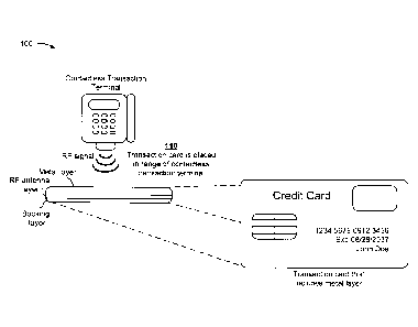
[0011] Figs. 1A-1C are diagrams of an overview of an example implementation
100
described herein. In example implementation 100 of Figs. 1A-1C a transaction
card is provided
for contactless transactions with a contactless transaction terminal (e.g., a
point of sale (PoS)
terminal). In Figs. 1A-1C, the transaction card includes a metal layer, an RF
antenna layer, and a
backing layer.
100121 As shown in Fig. IA, and by reference number 110, the transaction
card is placed
in range of the contactless transaction terminal. For example, the transaction
card may be placed
in range by a consumer (e.g., an individual named John Doe as shown on the
transaction card)
6
CA 3015273 2018-08-24
84450460
waving the transaction card over or near the contactless transaction terminal.
Accordingly, an
RF antenna of the RF antenna layer of the transaction card is in range of the
contactless
transaction terminal such that the RF antenna may be capable of transmitting
and/or receiving RF
signals to and/or from the contactless transaction terminal.
[0013] As shown in Fig. 1B, and by reference number 120, the metal layer of
the
transaction card captures eddy currents from the RF signal, preventing the RF
signal from
reaching the RF antenna, and thus preventing the RF antenna from communicating
data to the
contactless transaction terminal. For example, the RF signal may be absorbed
via the eddy
currents and/or the eddy currents may cause interference that prevents the RF
antenna from being
able to read and/or detect the RF signal. As shown in Fig. 1B, dense eddy
currents are present in
the metal layer of the transaction card. Accordingly, the dense eddy currents
prevent the RF
antenna in the RF antenna layer from communicating data (e.g., account
information, a payment
token, and/or the like) associated with the transaction card to the
contactless transaction terminal.
[0014] As shown in Fig. 1C, and by reference number 130, by including a
plurality of
holes in the metal layer of the transaction card, the density of the eddy
currents can be reduced,
thereby allowing the RF antenna to receive and/or transmit an RF signal.
Accordingly, the
transaction card of Fig. 1C is a different transaction card than the
transaction card of Fig. 1B.
The transaction card of Fig. 1C shows that eddy currents in the metal layer of
the transaction
card are less dense than the eddy currents in the transaction card of Fig. 1B.
Furthermore,
according to some implementations herein, the plurality of holes (and/or a
pattern of the plurality
of holes) may be configured to maintain the structural integrity of the
transaction card while
reducing the density of the eddy currents at the same time. For example, the
transaction cart of
Fig. 1C may have a threshold stiffness relative to the stiffness of the
transaction card of Fig. 1B
7
CA 3015273 2018-08-24
84450460
such that a difference in the stiffness between the transaction cards of Figs.
1B and 1C is
relatively unnoticeable.
[0015] As illustrated in example implementation 100 of Figs. 1A-1C, a
contactless
transaction card with a metal layer including a plurality of holes may be
provided to enable
contactless transaction with a contactless transaction terminal. Therefore,
some implementations
herein improve wireless communications between the contactless transaction
card and the
contactless transaction terminal by reducing a density of eddy currents in the
metal layer, while
maintaining the structural integrity of the transaction card and/or aesthetics
of the transaction
card, relative to a metal transaction card that does not include the plurality
of holes.
Accordingly, some implementations herein may conserve resources (e.g., power,
processing
capabilities, and/or the like) of a contactless transaction terminal by
reducing an amount of
communication failures between a metal contactless transaction card and the
transaction
terminal.
[0016] As indicated above, Figs. 1A-1C are provided merely as an example.
Other
examples are possible and may differ from what was described with regard to
Figs. 1A-1C.
[0017] Fig. 2 is a diagram of an example environment 200 in which devices
described
herein, may be implemented. As shown in Fig. 2, environment 200 may include a
transaction
card 210, a transaction terminal 220, a network 230, and a transaction backend
240. In
environment 200, transaction card 210 may communicate data associated with or
relating to a
transaction with transaction terminal 220, which facilitates processing the
transaction through
communication with transaction backend 240 via network 230. Devices of
environment 200
may interconnect via wired connections, wireless connections, or a combination
of wired and
wireless connections.
8
CA 3015273 2018-08-24
84450460
100181 Transaction card 210 includes a transaction card with a metal layer
containing a
plurality of holes. Transaction card 210 is capable of storing and/or
communicating data for a
PoS transaction with transaction terminal 220. For example, transaction card
210 may store or
communicate data including account information (e.g., an account identifier, a
cardholder
identifier, etc.), expiration information of transaction card 210, banking
information, transaction
information (e.g., a payment token), and/or the like. For example, to store or
communicate the
data, transaction card 210 may include a magnetic strip and/or an integrated
circuit (IC) chip
(e.g., a EUROPAY , MASTERCARD , VISA (EMV) chip). Transaction card 210 may
include an antenna to communicate data associated with transaction card 210.
The antenna may
be a passive RF antenna, an active RF antenna, and/or a battery-assisted RF
antenna. In some
implementations, transaction card 210 may be a smart transaction card, capable
of
communicating wirelessly (e.g., via Bluetooth, Bluetooth Low Energy (BLE),
and/or the like)
with a computing device, such as a smartphone, a digital wallet, and/or other
device.
100191 Transaction terminal 220 includes one or more devices capable of
receiving,
generating, storing, processing, and/or providing information associated with
facilitating a
transaction (a PoS transaction). For example, transaction terminal 220 may
include a
communication device and/or computing device capable of receiving data from
transaction card
210 and/or processing a transaction based on the data. In some
implementations, transaction
terminal 220 may include a desktop computer, a laptop computer, a tablet
computer, a handheld
computer, and/or a mobile phone (e.g., a smart phone, a radiotelephone, etc.).
Transaction
terminal 220 may be owned and/or operated by one or more individuals or
businesses engaged in
a sale of goods or services (e.g., one or more merchants, vendors, service
providers, and/or the
like).
9
CA 3015273 2018-08-24
84450460
[0020] Transaction terminal 220 may include one or more devices to
facilitate processing
a transaction via transaction card 210. Transaction terminal 220 may include a
PoS terminal, a
security access terminal, an ATM terminal, and/or the like. Transaction
terminal 220 may
include one or more input devices and/or output devices to facilitate
obtaining transaction card
data from transaction card 210 and/or interaction or authorization from a
cardholder of
transaction card 210. Example input devices of transaction terminal 220 may
include a number
keypad, a touchscreen, a magnetic strip reader, a chip reader, and/or an RF
signal reader. A
magnetic strip reader of transaction terminal 220 may receive transaction card
data as a magnetic
strip of transaction card 210 is swiped along the magnetic strip reader. A
chip reader of
transaction terminal 220 may receive transaction card data from an IC chip
(e.g., an EMV chip)
of transaction card 210 when the chip is placed in contact with the chip
reader. An RF signal
reader of transaction terminal 220 may enable contactless transactions from
transaction card 210
by obtaining transaction card data wirelessly from transaction card 210 as
transaction card 210
comes within a range of transaction terminal 220 that the RF signal reader may
detect an RF
signal from an RF antenna of transaction card 210. Example output devices of
transaction
terminal 220 may include a display device, a speaker, a printer, and/or the
like.
[0021] Network 230 includes one or more wired and/or wireless networks. For
example,
network 230 may include a cellular network (e.g., a long-term evolution (LTE)
network, a code
division multiple access (CDMA) network, a 3G network, a 4G network, a 5G
network, another
type of next generation network, etc.), a public land mobile network (PLNIN),
a local area
network (LAN), a wide area network (WAN), a metropolitan area network (MAN), a
telephone
network (e.g., the Public Switched Telephone Network (PSTN)), a private
network, an ad hoc
CA 3015273 2018-08-24
84450460
network, an intranet, the Internet, a fiber optic-based network, a cloud
computing network,
and/or the like, and/or a combination of these or other types of networks.
[0022] Transaction backend 240 includes one or more devices capable of
authorizing
and/or facilitating a transaction. For example, transaction backend 240 may
include one or more
servers and/or computers to store and/or provide information (e.g.,
authorizations, balances,
payment tokens, security information, account information, and/or the like)
associated with
processing a transaction via transaction terminal 220.
[0023] Transaction backend 240 may include one or more devices associated
with banks
and/or transaction card associations that authorize the transaction and/or
facilitate a transfer of
funds or payments between an account of a cardholder of transaction card 210
and an account of
an individual or business of transaction terminal 220. For example,
transaction backend 240 may
include one or more devices of one or more issuing banks associated with a
cardholder of
transaction card 210, one or more devices of one or more acquiring banks (or
merchant banks)
associated with transaction terminal 220, and/or one or more devices
associated with one or more
card associations (e.g., VISA , MASTERCARD , and/or the like) associated with
transaction
card 210. Accordingly, in response to receiving transaction card data
associated with transaction
card 210 from transaction terminal 220, various banking institutions and/or
card associations of
transaction backend 240 may communicate to authorize the transaction and/or
transfer funds
between the accounts associated with transaction card 210 and/or transaction
teiminal 220.
[0024] Transaction backend 240 may include one or more devices associated
with
security that may provide or deny authorization associated with the
transaction. For example,
transaction backend 240 may store and/or provide security access information
that may or may
not allow access through an access point (e.g., a gate, a door, and/or the
like) of a secure location
11
CA 3015273 2018-08-24
84450460
(e.g., a room, a building, an geographical area, a transportation terminal,
and/or the like) based
on information (e.g., account information, a key, an identifier, credentials,
and/or the like)
associated with transaction card 210 and/or provided by transaction terminal
220.
[0025] Transaction backend 240 may include one or more devices associated
with a
rewards program with transaction card 210 and/or an entity (e.g., a bank, a
merchant, a service
provider, a vendor, and/or the like) associated with the transaction card 210
and/or transaction
terminal 220 and/or an entity associated with transaction terminal 220. For
example, transaction
backend 240 may authorize the earning and/or redemption of rewards (e.g.,
rewards points
associated with transaction card 210, cash rewards, client loyalty rewards
associated with an
entity associated with transaction terminal 220, and/or the like) based on a
transaction processed
by transaction terminal 220 with transaction card 210.
100261 The number and arrangement of devices and networks shown in Fig. 2
are
provided as an example. In practice, there may be additional devices and/or
networks, fewer
devices and/or networks, different devices and/or networks, or differently
arranged devices
and/or networks than those shown in Fig. 2. Furthermore, two or more devices
shown in Fig. 2
may be implemented within a single device, or a single device shown in Fig. 2
may be
implemented as multiple, distributed devices. Additionally, or alternatively,
a set of devices
(e.g., one or more devices) of environment 200 may perform one or more
functions described as
being performed by another set of devices of environment 200.
100271 Fig. 3 is a diagram of an example implementation 300 of a metal
contactless
transaction card described herein. The transaction card, of example
implementation 300 of Fig.
3. may correspond to transaction card 210. In Fig. 3, the transaction card is
shown with a metal
12
CA 3015273 2018-08-24
84450460
layer, an RF antenna layer, and a backing layer. In the example implementation
of Fig. 3, the RF
antenna layer is positioned between the metal layer and the backing layer of
the transaction card.
[0028] As shown in Fig. 3, the RF antenna layer includes an RF antenna to
facilitate
communicating data relating to a transaction wirelessly via an RF signal
(e.g., an RF signal
communicated with transaction terminal 220). The metal layer, of the example
implementation
of Fig. 3, includes a plurality of holes (which may be referred to herein
collectively as "the
holes") to limit eddy currents (e.g., eddy currents caused by the RF signal)
in the metal layer to a
threshold density. For example, the threshold density may be a density that
corresponds to a
particular threshold of the amplitude of the RF signal. In some
implementations, the threshold
density may correspond to a percentage of a density of the eddy currents in
the metal layer
without the holes.
[0029] Furthermore, as shown in Fig. 3, the holes extend from a top surface
of the metal
layer to a bottom surface of the metal layer. In some implementations, the
holes may not extend
from the top surface of the metal layer to the bottom surface of the metal
layer. For example, the
holes may extend from the top surface to a middle plane of the metal layer
that is between the
top surface and the bottom surface of the metal layer. Additionally, or
alternatively, the holes
may extend from the bottom surface to the middle plane of the metal layer that
is between the top
surface and the bottom surface of the metal layer. In some implementations,
the holes may
include a subset of holes that extend from the top surface to the bottom
surface of the metal
layer, a subset of holes that extend from the top surface to the middle plane
of the metal layer,
and/or a subset of holes that extend from the bottom surface to the middle
plane of the metal
layer.
13
CA 3015273 2018-08-24
84450460
[0030] In some implementations, a threshold percentage (e.g., 50%, 80%,
100%, and/or
the like) of the holes may include a dielectric. For example, the holes may be
partially or
entirely filled with a dielectric. More specifically, the holes may be filled
with a nonconductive
material such that a surface of the material in the holes is on plane (within
a tolerance range)
with the top surface of the metal layer. In some implementations, an
identification film may be
included over the top surface of the metal layer. For example, the
identification film may
include identification information associated with the transaction card, such
as a cardholder's
name, an account number, an expiration date, a bank identifier, a card
association identifier,
and/or the like. Accordingly, the identification film may be included and/or
added to provide an
aesthetic look and indicate information associated with the transaction card.
[0031] In some implementations, the holes may be etched and/or drilled into
the metal
layer of the transaction card of Fig. 3. For example, the holes in the metal
layer of example
implementation 300 may be formed using a die cut process, a microcomputer
numerical control
(micro CNC) process, and/or a drill press. In some implementations, each of
the holes or some
of the holes (or at least the openings of the holes on the top surface) may
have substantially a
same shape (e.g., triangular, circular (cylindrical), square, rectangular,
polygonal, and/or the like)
and/or size. In some implementations, each of the holes or some of the holes
(or at least the
openings of the holes on the top surface) may have substantially a different
shape and/or size. In
some implementations, the holes may be equal to or less than one tenth of an
inch (or less than
approximately 3/32 of an inch or 2.3 millimeters (mm)) wide (e.g., may have a
diameter of less
than one tenth of an inch (or less than 2.3mm)).
[0032] The holes, in example implementation 300 of Fig. 3, may be
positioned in a
specified pattern. For example, the holes may be positioned in a specific
pattern (e.g., a random
14
CA 3015273 2018-08-24
84450460
pattern, a symmetrical pattern, etc.) associated with a particular symbol,
image, icon, shape,
and/or the like. In some implementations, the holes may be positioned in a
specified pattern to
maintain a threshold stiffness of the metal layer to provide structural
integrity to the transaction
card. For example, a threshold stiffness may correspond to a percentage of the
stiffness of the
metal layer (or transaction card) if the holes were not included in the metal
layer. Furthermore,
in some implementations, the holes may be positioned in a specified pattern
that corresponds to a
layout of the RF antenna layer. For example, the holes may be distributed
throughout the metal
layer to match a layout of the RF antenna in the RF antenna layer and/or to
match a location of
the RF antenna of the RF antenna layer.
[0033] In some implementations, a layout of the holes may be designed based
on the
layout of the RF antenna and/or RF antenna layer. Such a layout may be
designed based on the
design or characteristics of the RF antenna (e.g., active, passive, or battery
assisted),
characteristics of the RF antenna layer, characteristics of the metal layer
(e.g., a type of metal, a
type of metal alloy, or dimensions of the metal layer), dimensions of the
transaction card, and/or
the like. In some implementations, the holes may be positioned in a determined
optimal layout
designed to limit eddy currents to an optimal threshold density (e.g., a
density less than the
threshold density, such as a lowest possible eddy current density). As used
herein, an optimal
layout and/or optimal threshold density are considered optimal relative to the
design analysis
used to design the layout. In some implementations, simulations can be done to
determine the
optimal layout. For example, the holes can be moved and/or positioned, the
eddy currents may
then be determined based on the position of the holes and/or the structural
integrity of the metal
layer (and/or transaction card) may be determined based on the position of the
holes. Further,
CA 3015273 2018-08-24
84450460
the above may be repeated until an optimal layout of the holes (e.g., a
combination of lowest
eddy currents and best structural integrity) is found.
[0034] Accordingly, a transaction card with a metal layer is provided that
communicates
data relating to a transaction with a transaction terminal (e.g., transaction
terminal 220) while
limiting eddy currents in the metal layer to a threshold density. Furthermore,
some
implementations herein maintain structural integrity of the transaction card
by positioning a
plurality of holes in specified locations (or in a specified pattern)
throughout the metal layer.
[0035] As indicated above, Fig. 3 is provided merely as an example. Other
examples are
possible and may differ from what was described with regard to Fig. 3.
[0036] Fig. 4 is a diagram of an example implementation 400 of a metal
contactless
transaction card described herein. The transaction card of example
implementation 400 of Fig. 4
may correspond to transaction card 210. Similar to Fig. 3, in Fig. 4, the
transaction card is
shown with an RF antenna layer positioned between the metal layer and the
backing layer of the
transaction card.
[0037] In example implementation 400 of Fig. 4, a majority of the holes may
be
positioned in the metal layer in an area that corresponds to a position of the
RF antenna in the RF
antenna layer. For example, the holes may be positioned to overlap the RF
antenna. The greater
density of the holes lessens the density of the eddy currents in the
transaction card. Accordingly,
eddy currents may be less dense in the area of the metal layer that is
adjacent the RF antenna.
Accordingly, a greater density of a subset of the holes of the plurality of
holes may be closer to
an area of the metal layer that overlaps the RF antenna and a lesser density
of a subset of the
holes may be further from the area that overlaps the RF antenna. Therefore,
the transaction card
16
CA 3015273 2018-08-24
84450460
of example implementation 400 may facilitate communicating data associated
with a transaction
with a transaction terminal (e.g., transaction terminal 220).
[0038] As indicated above, Fig. 4 is provided merely as an example. Other
examples are
possible and may differ from what was described with regard to Fig. 4.
[0039] Fig. 5 is a diagram of an example implementation 500 of a metal
contactless
transaction card described herein. The transaction card of example
implementation 500 of Fig. 5
may correspond to transaction card 210. Similar to Figs. 3 and 4, in Fig. 5,
the transaction card
is shown with an RF antenna layer positioned between the metal layer and the
backing layer of
the transaction card. In example implementation 500, the backing layer may be
comprised of a
metal or primarily of a metal.
[0040] In example implementation 500 of Fig. 5, the backing layer includes
a plurality of
holes (labeled as backing layer holes). As shown, the backing layer holes
overlap the holes of
the metal layer. For example, the holes of the metal layer and the backing
layer holes may be
positioned to match one another (within a tolerance range) relative to the
layout or dimensions of
the transaction card of example implementation 500. In some implementations, a
subset of holes
of the metal layer may overlap a subset of the backing layer holes, while
another subset of the
holes of the metal layer do not overlap another subset of the backing layer
holes. According to
some implementations, the backing layer holes may be positioned in a specified
pattern similar
to the holes of the metal layer. The specified pattern of the backing holes
may match or not
match the specified pattern of the holes of the metal layer.
100411 In some implementations, the backing layer holes may or may not be a
same size
and/or shape as the holes of the metal layer. Additionally, alternatively, the
a subset of the
backing layers holes may be a same size and/or shape as some of holes of the
metal layer and
17
CA 3015273 2018-08-24
84450460
another subset of the backing layer holes may not be the same size and/or
shape as some of the
holes of the metal layer. Furthermore, a density of the backing layer holes
may or may not
match a density of the holes of the metal layer. In some implementations, a
quantity of the
backing layer holes may or may not match a quantity of the holes of the metal
layer.
[0042] Accordingly, the transaction card of example implementation 500 may
wirelessly
communicate data relating to a transaction while limiting eddy currents in the
metal layer and/or
in the metal backing layer of the transaction card. Furtheintore, the metal
backing layer of
example implementation 500 may provide additional stiffness and/or increase a
structural
integrity of the transaction card relative to the backing layer being a
plastic or other non-metallic
material.
[0043] As indicated above, Fig. 5 is provided merely as an example. Other
examples are
possible and may differ from what was described with regard to Fig. 5.
100441 Fig. 6 is a diagram of an example implementation 600 of a metal
contactless
transaction card described herein. As shown in Fig. 6, a plurality of holes
are included in a metal
layer. The metal layer of example implementation 600 may be a metal layer of
transaction card
210. In Fig. 6, a perimeter of the holes that defines an area of the holes in
example
implementation 600 is shown. In some implementations, the area of the holes
defined by the
perimeter of the holes may be a threshold area of the metal layer (and/or the
transaction card).
For example, the area of the holes may be at least 50% (or 75% or 95%, etc.)
of the area of the
metal layer (and/or of the transaction card). In some implementations, a
combined surface area
of the holes may be a threshold area of an area of the metal layer defined by
the perimeter of the
holes. For example, a total of the surface areas of the holes in example
implementation 600 is to
be at least 10% (or 20% or 30%) of the area of the perimeter of the holes.
18
CA 3015273 2018-08-24
84450460
[0045] Furthermore, the holes of example implementation 600 are shown in a
specified
shape (i.e., a rectangular shape). As shown, the holes may be equidistant from
one another in the
particular shape. In some implementations, distances between holes in a
particular shape may
increase or decrease based on a density of the holes within the pattern.
though the pattern may
maintain the specified shape. In some implementations, the holes of the metal
layer may not be
evenly distributed. In some implementations, the holes may appear to have a
random pattern.
[0046] In some implementations, the position of the holes in the metal
layer of example
implementation 600 may be positioned without regard to the RF antenna area.
Accordingly, the
layout of the holes may not depend on the layout of the RF antenna and/or the
RF antenna layer.
[0047] Accordingly, a pattern of holes in a metal layer of a transaction
card may enable
the transaction card to wirelessly communicate data associated with a
transaction with a
transaction terminal processing the transaction.
[0048] As indicated above, Fig. 6 is provided merely as an example. Other
examples are
possible and may differ from what was described with regard to Fig. 6.
[0049] Fig. 7 is a diagram of an example implementation 700 of a metal
contactless
transaction card described herein. As shown in Fig. 7, a plurality of holes
are included in a metal
layer. The metal layer of example implementation 700 may be a metal layer of
transaction card
210. In Fig. 7, a perimeter of the holes that defines an area of the holes in
example
implementation 700 is shown. As shown, the holes are positioned in the metal
layer such that
the perimeter of the area of the holes overlaps a perimeter of the RF antenna
in the RF antenna
layer. In some implementations, the perimeter of the area of the holes (or the
area of the holes)
may be less than or greater than the perimeter of the area of the RF antenna
(or the area of the RF
antenna).
19
CA 3015273 2018-08-24
84450460
[0050] Accordingly, a pattern of holes in a metal layer that is based on a
location of an
RF antenna of a transaction card may enable the transaction card to wirelessly
communicate data
associated with a transaction with a transaction terminal processing the
transaction.
[0051] As indicated above, Fig. 7 is provided merely as an example. Other
examples are
possible and may differ from what was described with regard to Fig. 7.
[0052] Fig. 8 is a diagram of an example implementation 800 of a metal
contactless
transaction card described herein. As shown in Fig. 8, a plurality of holes
are included in a metal
layer. The metal layer of example implementation 800 may be a metal layer of
transaction card
210. In Fig. 8, an RF antenna area is shown. Further, as shown, the holes are
positioned in a
specified pattern in which the holes are more densely positioned over the RF
antenna area and
less densely positioned in the area outside of the RF antenna layer.
Accordingly, a first subset of
the holes are positioned in a greater density over the RF antenna in the RF
antenna layer than a
second subset of the holes that are not positioned over the RF antenna in the
RF antenna layer.
In some implementations, the pattern may include a greater density of holes
closer to the center
of the RF antenna area and a lesser density of holes farther from the center
of the RF antenna
area. In some implementations, the pattern of the holes may be dependent on a
configuration or
design of the RF antenna, as shown in Fig. 8.
[0053] Accordingly, a pattern of holes in a metal layer that is based on a
location and/or
configuration of an RF antenna of a transaction card may enable the
transaction card to
wirelessly communicate data associated with a transaction with a transaction
terminal processing
the transaction.
[0054] As indicated above, Fig. 8 is provided merely as an example. Other
examples are
possible and may differ from what was described with regard to Fig. 8.
CA 3015273 2018-08-24
84450460
[0055] Fig. 9 is a diagram of an example implementation 900 of a metal
contactless
transaction card described herein. As shown in Fig. 9, a plurality of holes
are included in a metal
layer. The metal layer of example implementation 900 may be a metal layer of
transaction card
210. In Fig. 9, an RF antenna area is shown. Further, as shown, the holes are
positioned in
specified patterns in which the holes outside of the RF antenna are positioned
in a first pattern
(e.g., a rectangle) and the holes inside the RF antenna area are positioned in
diamond (or arrow)
patterns that get more dense as the pattern approaches the center of the RF
antenna area.
[0056] Accordingly, a plurality of patterns of holes in a metal layer that
are based on a
location of an RF antenna of a transaction card may enable the transaction
card to wirelessly
communicate data associated with a transaction with a transaction terminal
processing the
transaction.
[0057] As indicated above, Fig. 9 is provided merely as an example. Other
examples are
possible and may differ from what was described with regard to Fig. 9.
[0058] According to some implementations herein, a metal, contactless
transaction card
is provided with a plurality of holes in one or more metal layers of the
transaction card. The
plurality of holes in the metal layer limit eddy currents in the metal layer
to a threshold density.
Accordingly, the eddy currents in the metal layer of the transaction card are
too weak to interfere
with an RF signal used for communicating data associated with the transaction
card with a
transaction terminal. Furthermore, the plurality of holes may be positioned in
a pattern to
maintain the aesthetics and structural integrity of the transaction card
relative to a metal
transaction card that does not include the plurality of holes.
[0059] The foregoing disclosure provides illustration and description, but
is not intended
to be exhaustive or to limit the implementations to the precise form
disclosed. Modifications and
21
CA 3015273 2018-08-24
84450460
variations are possible in light of the above disclosure or may be acquired
from practice of the
implementations.
[0060] As used herein, the term component is intended to be broadly
construed as
hardware, firmware, or a combination of hardware and software.
[0061] Some implementations are described herein in connection with
thresholds. As
used herein, satisfying a threshold may refer to a value being greater than
the threshold, more
than the threshold, higher than the threshold, greater than or equal to the
threshold, less than the
threshold, fewer than the threshold, lower than the threshold, less than or
equal to the threshold,
equal to the threshold, or the like.
[0062] Even though particular combinations of features are recited in the
claims and/or
disclosed in the specification, these combinations are not intended to limit
the disclosure of
possible implementations. In fact, many of these features may be combined in
ways not
specifically recited in the claims and/or disclosed in the specification.
Although each dependent
claim listed below may directly depend on only one claim, the disclosure of
possible
implementations includes each dependent claim in combination with every other
claim in the
claim set.
[0063] No element, act, or instruction used herein should be construed as
critical or
essential unless explicitly described as such. Also, as used herein, the
articles "a" and "an" are
intended to include one or more items, and may be used interchangeably with
"one or more."
Furthermore, as used herein, the term "set" is intended to include one or more
items (e.g., related
items, unrelated items, a combination of related and unrelated items, etc.),
and may be used
interchangeably with "one or more." Where only one item is intended, the term
"one" or similar
language is used. Also, as used herein, the terms "has," "have," "having," or
the like are
22
CA 3015273 2018-08-24
84450460
intended to be open-ended terms. Further, the phrase "based on" is intended to
mean "based, at
least in part, on" unless explicitly stated otherwise.
23
CA 3015273 2018-08-24