Note: Descriptions are shown in the official language in which they were submitted.
INDUCTOR ASSEMBLIES
RELATED APPLICATION(S)
[001] The present application claims the benefit of and priority from U.S.
Provisional
Patent Application No. 62/557,289, filed September 12, 2017.
FIELD OF THE INVENTION
[002] The present invention relates to inductor assemblies and, more
particularly, to
inductor assemblies including inductor coils and methods for making the same.
BACKGROUND OF THE INVENTION
[003] Inductors coils are used in the AC power networks for power factor
correction,
voltage regulation, reduction of di/dt, and protection of downstream
equipment.
SUMMARY OF THE INVENTION
[004] According to embodiments of the invention, an inductor assembly includes
a
coil including a spirally wound metal foil.
[005] In some embodiments, the coil has a longitudinal coil axis and a radial
coil
thickness, the metal foil has a foil width extending substantially parallel to
the coil axis, and
the foil width is greater than the coil thickness.
[006] In some embodiments, the metal foil has a foil thickness in the range of
from
about 0.5 mm to 1 mm.
[007] In some embodiments, the coil includes an electrical insulator layer
spirally co-
wound with the metal foil.
[008] In some embodiments, the electrical insulator layer has a thickness in
the range
of from about 0.05 to 1 mm.
[009] In some embodiments, the ratio of the foil width to the foil thickness
is in the of
from about 170 to 500.
[0010] According to some embodiments, the metal foil and the electrical
insulator
layer are not bonded to one another across their widths.
[0011] In some embodiments, the coil has a substantially cylindrical outer
profile.
[0012] According to some embodiments, the inductor assembly includes an
electrically insulating epoxy resin surrounding and engaging the coil.
1
Date Recue/Date Received 2022-02-20
[0013] In some embodiments, the inductor assembly further includes a second
coil
including a second spirally wound metal foil, and the epoxy resin surrounds
and engages the
second coil, and is interposed between the first and second coils.
[0014] According to some embodiments, the inductor assembly includes an
enclosure
defining an enclosed chamber, wherein the coil is disposed in the chamber.
[0015] In some embodiments, the inductor assembly includes at least one
mounting
bracket supporting the enclosure and the coil.
[0016] According to some embodiments, the inductor assembly includes a
terminal
bus bar electrically connected to the metal foil and including a terminal, and
an electrically
insulating heat shrunk tube surrounding a portion of the terminal bus bar.
[0017] In some embodiments, the coil includes a second metal foil spirally co-
wound
with the first metal foil to form a multilayer conductor.
[0018] In some embodiments, the coil includes an electrical insulator layer
spirally
co-wound with the first and second metal foils.
[0019] According to some embodiments, the first and second metal foils and the
electrical insulator layer are not bonded to one another across their widths.
[0020] According to some embodiments, the coil has a coil longitudinal axis,
the coil
has an innermost winding of the metal foil and an outermost winding of the
metal foil, the
inductor assembly includes a first terminal bus bar connected to the innermost
winding and
projecting outwardly from an axial end of the inductor assembly, and the
inductor assembly
includes a second terminal bus bar connected to the outermost winding and
projecting
outwardly from the axial end of the inductor assembly.
[0021] According to embodiments of the invention, a multi-unit inductor system
includes first and second inductor assemblies. The first inductor assembly
includes a first
coil, the first coil including a spirally wound first metal foil. The second
inductor assembly
includes a second coil, the second coil including a spirally wound second
metal foil. The first
coil is electrically connected to the second coil.
[0022] In some embodiments, the first coil has a first coil longitudinal axis
and the
second coil has a second coil longitudinal axis. Each of the first and second
inductor
assemblies includes: a first terminal bus bar connected to the coil thereof
and projecting
outwardly from an axial end of the inductor assembly; and a second terminal
bus bar
connected to the coil thereof and projecting outwardly from the axial end of
the inductor
assembly. The first and second inductor assemblies are positioned side-by-side
and the first
2
CA 3015864 2018-08-30
terminal bus bar of the second inductor assembly is electrically connected to
the
second terminal bus bar of the first inductor assembly.
[0023] According to embodiments of the invention, a method for forming an
inductor
assembly includes spirally winding a metal foil into the form of a coil.
[0024] In some embodiments, the method includes spirally co-winding an
electrical
insulator sheet with the metal foil.
[0025] According to some embodiments, the metal foil and the electrical
insulator
sheet are not bonded to one another during the step of co-winding the
electrical insulator
sheet and the metal foil.
[0025a] In another aspect, there is provided a inductor assembly comprising: a
coil
including a spirally wound first metal foil; a second metal foil spirally co-
wound in face-to-
face electrical contact with the first metal foil to form a multilayer
conductor; and an
electrical insulator sheet spirally co-wound with the first and second metal
foils; wherein: the
first metal foil and the second metal foil are not bonded to one another
across their widths;
and the first metal foil and the second metal foil are not bonded to the
electrical insulator
sheet across their widths.
10025b] In yet another aspect, there is provided a multi-unit inductor system
comprising: a first inductor assembly including a first coil, the first coil
including a spirally
wound first metal foil; and a second inductor assembly including a second
coil, the second
coil including a spirally wound second metal foil; wherein the first coil is
electrically
connected to the second coil; and wherein: the first coil has a first coil
longitudinal axis; the
second coil has a second coil longitudinal axis; each of the first and second
inductor
assemblies includes: a first terminal bus bar connected to the coil thereof
and projecting
outwardly from an axial end of the inductor assembly; and a second terminal
bus bar
connected to the coil thereof and projecting outwardly from the axial end of
the inductor
assembly; wherein the first and second inductor assemblies are positioned side-
by-side and
the first terminal bus bar of the second inductor assembly is electrically
connected to the
second terminal bus bar of the first inductor assembly.
10025c] In yet another aspect, there is provided a method for forming an
inductor
assembly, the method comprising: spirally co-winding a first metal foil, a
second metal foil,
and an electrical insulator sheet; wherein the first metal foil and the second
metal foil are co-
wound in face-to-face electrical contact with one another to form a multilayer
conductor; and
wherein, during the step of spirally co-winding the first metal foil, the
second metal foil, and
the electrical insulator sheet: the first metal foil and the second metal foil
are not bonded to
3
Date Recue/Date Received 2022-02-20
one another across their widths; and the first metal foil and the second metal
foil are not
bonded to the electrical insulator sheet across their widths.
[0025d] In still another aspect, there is provided an inductor assembly
comprising:
a coil including a spirally wound metal foil; a terminal bus bar electrically
connected to the
metal foil and including a terminal; and an electrically insulating polymeric
tube surrounding
a portion of the terminal bus bar.
BRIEF DESCRIPTION OF THE DRAWINGS
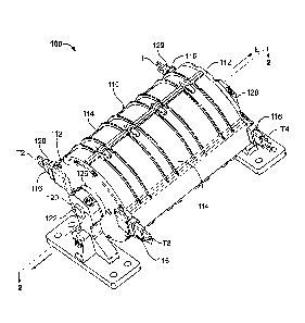
[0026] FIG. 1 is a top, perspective view of an inductor assembly according to
embodiments of the invention.
[0027] FIG. 2 is a cross-sectional view of the inductor assembly of FIG. 1
taken
along the line 2-2 of FIG. 1.
[0028] FIG. 3 is a perspective view of the inductor assembly of FIG. 1 wherein
shells
of the inductor assembly are removed for the purpose of explanation.
[0029] FIG. 4 is a perspective view of the inductor assembly of FIG. 1 wherein
the
shells and potting of the inductor assembly are removed for the purpose of
explanation.
[0030] FIG. 5 is a perspective view of the inductor assembly of FIG. 1 wherein
the
shells, the potting and coils of the inductor assembly are removed for the
purpose of
explanation.
[0031] FIG. 6 is a perspective view of a coil assembly forming a part of the
inductor
assembly of FIG. 1.
[0032] FIG. 7 is a side view of the coil assembly of FIG. 6.
[0033] FIG. 8 is an end view of the coil assembly of FIG. 6.
[0034] FIG. 9 is an enlarged, fragmentary, cross-sectional view of the coil
assembly
of FIG. 6.
[0035] FIG. 10 is a fragmentary, perspective view of a conductor foil and an
insulator
sheet forming parts of the coil assembly of FIG. 6, wherein the conductor foil
and the
insulator sheet are shown flattened out for the purpose of explanation.
[0036] FIG. 11 is an electrical diagram representing a two-phase AC electrical
power
system including the inductor assembly of FIG. 1.
3a
Date Recue/Date Received 2022-02-20
[0037] FIG. 12 is a perspective view of an inductor assembly according to
further
embodiments of the invention.
[0038] FIG. 13 is a cross-sectional view of the inductor assembly of FIG. 12
taken
along the line 13-13 of FIG. 12.
[0039] FIG. 14 is an electrical diagram representing an electrical power
system
including the inductor assembly of FIG. 12.
[0040] FIG. 15 is a perspective view of an inductor assembly according to
further
embodiments of the invention.
[0041] FIG. 16 is a cross-sectional view of the inductor assembly of FIG. 15
taken
along the line 16-16 of FIG. 15.
[0042] FIG. 17 is a perspective view of the inductor assembly of FIG. 15
wherein
shells of the inductor assembly are removed for the purpose of explanation.
[0043] FIG. 18 is a perspective view of the inductor assembly of FIG. 15
wherein the
shells, potting and coils of the inductor assembly are removed for the purpose
of explanation.
[0044] FIG. 19 is a perspective view of a coil assembly forming a part of the
inductor
assembly of FIG. 15.
[0045] FIG. 20 is an exploded, perspective view of the coil assembly of FIG.
19.
[0046] FIG. 21 is an enlarged, fragmentary, end view of the coil assembly of
FIG.
19.
[0047] FIG. 22 is an enlarged, fragmentary, end view of the coil assembly of
FIG.
19.
[0048] FIG. 23 is a side view of the coil assembly of FIG. 19.
[0049] FIG. 24 is a perspective view of a multi-unit inductor system including
a
plurality of the inductor assemblies of FIG. 15.
[0050] FIG. 25 is a schematic diagram a multi-unit inductor system including a
plurality of the inductor assemblies of FIG. 1.
[0051] FIG. 26 is a schematic diagram of the multi-unit inductor system of
FIG. 5.
[0052] FIG. 27 is a perspective view of an inductor assembly according to
further
embodiments of the invention.
[0053] FIG. 28 is a cross-sectional view of the inductor assembly of FIG. 27
taken
along the line 28-28 of FIG. 27.
[0054] FIG. 29 is a perspective view of a multi-unit inductor system including
a
plurality of the inductor assemblies of FIG. 27.
4
CA 3015864 2018-08-30
[0055] FIG. 30 is a perspective view of a coil assembly according to further
embodiments of the invention.
[0056] FIG. 31 is an exploded, perspective view of the coil assembly of FIG.
30.
[0057] FIG. 32 is a side view of the coil assembly of FIG. 30.
[0058] FIG. 33 is an enlarged, fragmentary, end view of the coil assembly of
FIG.
30.
[0059] FIG. 34 is an enlarged, fragmentary, end view of the coil assembly of
FIG.
30.
DETAILED DESCRIPTION OF EMBODIMENTS OF THE INVENTION
[0060] The present invention now will be described more fully hereinafter with
reference to the accompanying drawings, in which illustrative embodiments of
the invention
are shown. In the drawings, the relative sizes of regions or features may be
exaggerated for
clarity. This invention may, however, be embodied in many different forms and
should not
be construed as limited to the embodiments set forth herein; rather, these
embodiments are
provided so that this disclosure will be thorough and complete, and will fully
convey the
scope of the invention to those skilled in the art.
[0061] It will be understood that, although the terms first, second, etc. may
be used
herein to describe various elements, components, regions, layers and/or
sections, these
elements, components, regions, layers and/or sections should not be limited by
these terms.
These terms are only used to distinguish one element, component, region, layer
or section
from another region, layer or section. Thus, a first element, component,
region, layer or
section discussed below could be termed a second element, component, region,
layer or
section without departing from the teachings of the present invention.
[0062] Spatially relative terms, such as "beneath", "below", "lower", "above",
"upper" and the like, may be used herein for ease of description to describe
one element or
feature's relationship to another element(s) or feature(s) as illustrated in
the figures. It will be
understood that the spatially relative terms are intended to encompass
different orientations of
the device in use or operation in addition to the orientation depicted in the
figures. For
example, if the device in the figures is turned over, elements described as
"below" or
"beneath" other elements or features would then be oriented "above" the other
elements or
features. Thus, the exemplary term "below" can encompass both an orientation
of above and
below. The device may be otherwise oriented (rotated 900 or at other
orientations) and the
spatially relative descriptors used herein interpreted accordingly.
CA 3015864 2018-08-30
[0063] As used herein, the singular forms "a", "an" and "the" are intended to
include
the plural forms as well, unless expressly stated otherwise. It will be
further understood that
the terms "includes," "comprises," "including" and/or "comprising," when used
in this
specification, specify the presence of stated features, integers, steps,
operations, elements,
and/or components, but do not preclude the presence or addition of one or more
other
features, integers, steps, operations, elements, components, and/or groups
thereof. It will be
understood that when an element is referred to as being "connected" or
"coupled" to another
element, it can be directly connected or coupled to the other element or
intervening elements
may be present. As used herein, the term "and/or" includes any and all
combinations of one
or more of the associated listed items.
[0064] Unless otherwise defined, all terms (including technical and scientific
terms)
used herein have the same meaning as commonly understood by one of ordinary
skill in the
art to which this invention belongs. It will be further understood that terms,
such as those
defined in commonly used dictionaries, should be interpreted as having a
meaning that is
consistent with their meaning in the context of this specification and the
relevant art and will
not be interpreted in an idealized or overly formal sense unless expressly so
defined herein.
[0065] Typical inductance coil designs use a conductor which is insulated
using a
varnish and is turned around a spool. However, such designs typically will not
be able to
withstand significant transient overvoltages between the turns of the coil and
will be large in
size, as the load current requires a significant cross-section of the
conductor. In that case,
there is a significant space lost in between the turns of the conductor, as it
has a round shape.
If an insulation cover were mounted over the coil to ensure that it can
withstand very high
transient overvoltages, then the overall coil assembly would become even
larger in size.
Further, vibration might be an issue as there is minimal contact between the
turns of the coil,
allowing some possible movement.
[0066] With reference to FIGS. 1-11 a dual coil inductor assembly 100
according to
embodiments of the invention is shown therein. The inductor assembly 100 has a
longitudinal axis L-L.
[0067] The inductor assembly 100 includes an enclosure 110, a pair of axially
spaced
apart support bases 120, a support shaft 122, an electrically insulating
fitting 124, a pair of
bushings 126, potting 128, insulation sleeves or tubes 129, a first coil
assembly 131, and a
second coil assembly 151.
[0068] The bases 120 and shaft 122 are metal (in some embodiments, aluminum).
The shaft 122 is supported by and affixed to the bases 120 at either end.
6
CA 3015864 2018-08-30
[0069] The fitting 124 is mounted around the shaft 122. The fitting 124 may be
formed of a plastic or polymeric material such as Polyethersulfone with a
dielectric strength
in the range of from about 30 to 40 kV/mm.
[0070] The coil assemblies 131, 151 (described in more detail below) are
mounted on
the fitting 124 and the shaft 122. The coil assemblies 131, 151 each include a
pair of terminal
bus bars 140, 142, 160, 162.
[0071] The enclosure 110 includes a pair of laterally opposed shells 114 and a
pair of
axially opposed end plates 112 that are fastened together to form the
enclosure 110. The
enclosure 110 defines an internal cavity or chamber 118 within which the
support shaft 122,
the fitting 124, the potting 128, the insulation tubes 129, the first coil
assembly 131, and the
second coil assembly 151 are disposed and contained. Four terminal openings
116 are
defined in the enclosure 110 and communicate with the chamber 118.
[0072] The enclosure components 112, 114 may be formed of any suitable
material.
In some embodiments, the enclosure components 112, 114 are formed of an
electrically
insulating polymeric flame retardant material such as Noryl N190X by SABIC
with a
dielectric strength of about 19 kV/mm.
[0073] Each of the four insulation tubes 129 surrounds a length of a
respective
terminal bus bar 140, 142, 160, 162 extending through the chamber 118, through
a terminal
opening 116, and beyond the terminal opening 116 a prescribed distance. The
tubes 129 may
be formed of any suitable material. In some embodiments, the tubes 129 are
formed of an
electrically insulating polymeric material. In some embodiments, the tubes 129
are formed of
an electrically insulating elastomeric material. In some embodiments, the
tubes 129 are
formed of an electrically insulating heat shrinkable polymer (e.g., elastomer)
that has been
heat shrunk about the corresponding terminal bus bar 140, 142, 160, 162.
[0074] The potting 128 fills the void space within the chamber 118 that is not
occupied by the other components. The potting 128 may formed of any suitable
material.
The potting 128 is electrically insulating. In some embodiments, the potting
128 is formed of
a material having a breakdown voltage of at least 18 kV/mm. In some
embodiments, the
potting 128 is an epoxy resin or a Polyurethane resin.
[0075] Each bushing 126 is annular and is sandwiched or interposed between an
end
plate 112 and the adjacent base 120 and mounted on the shaft 122. The bushings
126 may be
formed of any suitable material. In some embodiments, the bushings are formed
of a resilient
polymeric material. In some embodiments, the bushings 126 are formed of an
elastomer and,
in some embodiments, a silicone elastomer or rubber.
7
CA 3015864 2018-08-30
[0076] The coil assembly 131 includes a multi-layer coil 130, an inner
terminal bus
bar 140, and an outer terminal bus bar 142.
[0077] The coil 130 is an air core coil. The coil 130 has a coil axis A-A and
axially
opposed ends 130A, 130B. The coil 130 includes an electrically conductive
conductor sheet,
strip or foil 132 and an electrically insulative insulator strip or sheet 134.
The foil 132 and
sheet 134 are spirally co-wound or wrapped about the axis A-A to form windings
136. The
windings 136 extend progressively from an innermost winding 136E of the
conductor foil
132 in an inner passage 138 to an outermost winding 136F of the conductor foil
132 on the
outer diameter of the coil 130. Each winding 136 is radially superimposed on,
stacked on, or
wrapped around the preceding winding 136.
[0078] The conductor foil 132 has opposed side edges 132A that are axially
spaced
apart along the coil axis A-A and extend substantially parallel to one
another. The conductor
foil 132 is spirally wound such that each edge 132A remains substantially in
or proximate a
single lateral plane E-E (FIG. 7) throughout the coil 130 from the winding
136E to the
winding 136F. That is, the conductor foil 132 is maintained in alignment with
itself and is
spirally, not helically, wound.
[0079] According to some embodiments, the coil 130 includes at least 10 turns
or
windings from the winding 136E to the winding 136F and, in some embodiments,
from about
60 to 100 turns. It will be appreciated that in the figures the layers 132,
134 and turns of the
coils 130, 150 are not specifically shown or, in FIG. 8, are only partially
shown. As such, the
depictions of the layers 132, 134 in the drawings may not be to scale with
regard to the
number of turns, the thicknesses of the layers, or the spacing between layers.
[0080] The conductor foil 132 may be formed of any suitable electrically
conductive
material. In some embodiments, the conductor foil 132 is formed of metal. In
some
embodiments, the conductor foil 132 is formed of copper or aluminum.
[0081] The insulator sheet 134 may be formed of any suitable electrically
insulative
material. In some embodiments, the insulator sheet 134 is formed of a
polymeric material.
In some embodiments, the insulator sheet 134 is formed of polyester film. In
some
embodiments, the insulator sheet 134 is formed of a material having a
breakdown voltage of
at least 4 kV/mm and, in some embodiments, in the range of from about 13 kV/mm
to 20
kV/mm.
[0082] The coil 130 is generally tubular. In some embodiments, the outer
profile of
the coil 130 is substantially cylindrical and is substantially circular in
lateral cross-section.
8
CA 3015864 2018-08-30
[0083] The coil 130 has a thickness CT (FIG. 7), a length CL (FIG. 7; parallel
with
the coil axis L-L), and an outer diameter CD (FIG. 8). The thickness CT is the
radial
distance from the innermost conductor winding 136E to the outermost conductor
winding
136F in a lateral plane N-N (FIG. 7) orthogonal to the coil axis A-A.
100841 According to some embodiments, the coil 130 is generally cylindrical
with a
length CL greater than its outer diameter CD. According to some embodiments,
the ratio
CL/CD is at least 0,2 and, in some embodiments, is in the range of from about
0.3 to 1.5.
[0085] FIGS. 9-10 are fragmentary views of the conductor foil 132 and the
insulator
sheet 134 laid flat (e.g., prior to winding into the coil 130). The conductor
foil 132 has a
thickness MT, a length ML, and a width MW. The insulator sheet 134 has a
thickness IT, a
length IL, and a width IW.
[0086] According to some embodiments, the conductor foil width MW is greater
than
the coil outer diameter CD. In some embodiments, the ratio MW/CD is at least
0.2 and, in
some embodiments, is in the range of from about 0.4 to 1.5.
[0087] According to some embodiments, the conductor foil width MW is greater
than
the coil thickness CT. In some embodiments, the ratio MW/CT is at least 0.5
and, in some
embodiments, is in the range of from about 2 to 3.
[0088] According to some embodiments, the thickness MT is in the range of from
about 0.1 to 2 mm and, in some embodiments, in the range of from about 0.5 mm
to 1 mm.
According to some embodiments, the length ML is in the range of from about 1 m
to 40 m.
According to some embodiments, the width MW is in the range of from about 0.5
cm to 30
cm.
[0089] According to some embodiments, the thickness IT is in the range of from
about 0.05 to 1 mm. According to some embodiments, the length IL is in the
range of from
about 1 m to 40 m. According to some embodiments, the width IW is in the range
of from
about 0.5 cm to 30 cm.
[0090] According to some embodiments, the ratio MW/MT is at least 2.5 and, in
some embodiments, is in the range of from about 170 to 500.
[0091] According to some embodiments, the ratio 1W/IT is at least 2.5 and, in
some
embodiments, is in the range of from about 1000 to 4000.
[0092] According to some embodiments, edge sections 134G of the insulator
sheet
134 extend axially outwardly beyond the adjacent edges of the conductor foil
132 a distance
(FIG. 7). In some embodiments, the distance 10 is at least 1 mm and, in some
embodiments, is in the range of from about 3 mm to 10 mm.
9
CA 3015864 2018-08-30
[0093] According to some embodiments, the coil 130 is formed by the following
method. The conductor foil 132 is individually formed as a discrete tape,
strip, sheet or foil.
The insulator sheet 134 is separately individually formed as a discrete tape,
strip, sheet or
foil. The preformed foil 132 and preformed sheet 134 are thereafter mated,
laminated or
layered together and spirally co-wound into the coil configuration to form the
coil 130. In
some embodiments, the layers 132, 134 are co-wound about a cylindrical
mandrel, form or
support. In some embodiments, the layers 132, 134 are co-wound about the
fitting 124.
[0094] In some embodiments, the foil 132 and the sheet 134 are not bonded to
one
another along their lengths prior to winding into the coil. That is, the foil
132 and the sheet
134 are loosely co-wound and are not bonded or laminated to one another until
after
formation of the coil 130. In some embodiments, the foil 132 and the sheet 134
are not
bonded to one another in the completed coil 130 except by the potting 128 at
the ends of the
coil 130. Thus, in this case, the foil 132 and the sheet 134 are not bonded to
one another
across their widths. In some embodiments, the foil 132 and the sheet 134 are
tightly wound so
that air gaps between the windings of the conductor foil 132 are minimized or
eliminated.
[0095] The terminal bus bars 140, 142 may be formed of any suitable
electrically
conductive material. In some embodiments, the terminal bus bars 140, 142 are
formed of
metal. In some embodiments, the terminal bus bars 140, 142 are formed of
copper or tin-
plated copper.
[0096] The inner terminal bus bar 140 (FIG. 2) includes a contact leg 140A and
a
terminal leg Ti joined by a connector leg 140B. The contact leg 140A is
secured in
mechanical and electrical contact with the innermost winding 136E of the
conductor foil 132
by screws 5, nuts 6, and a clamping member or plate 141 (FIG. 8). The
conductor foil
winding 136E is interposed or sandwiched between the contact leg 140A and the
clamping
plate 141. The screws 5 penetrate through the winding 136E and are secured by
the nuts 6
such that the contact leg 140A and the clamping plate 141 compressively clamp
onto the
winding 136E therebetween. The terminal leg Ti extends out of the enclosure
110 through
an opening 116.
[0097] The outer terminal bus bar 142 (FIG. 2) includes a contact leg 142A and
a
terminal leg T2 joined by a connector leg 142B. The contact leg 142A is
secured in
mechanical and electrical contact with the outermost winding 136F of the
conductor foil 132
by screws 5, nuts 6, and a clamping plate 141 (FIG. 5). The winding 136F is
clamped
between the contact leg 142A and the clamping plate 141 by the screws 5 (which
penetrate
through the winding 136F) and the nuts 6 in the same manner as described above
for the
CA 3015864 2018-08-30
contact leg 140A, the screws 5, the nuts 6, and the clamping plate 141. The
terminal leg T2
extends out of the enclosure 110 through an opening 116.
[0098] The coil assembly 151 is constructed in the same manner as the coil
assembly
131 and includes a multi-layer coil 150, an inner terminal bus bar 160, and an
inner terminal
bus bar 162 corresponding to the 130, the inner terminal bus bar 140, and the
outer terminal
bus bar 142. The coil 150 has a coil axis B-B.
[0099] The terminal leg T3 of the inner terminal bus bar 160 is secured in
mechanical
and electrical contact with the innermost winding 156E of the conductor foil
of the coil 150
by screws 5, nuts 6, and a clamping plate 141 in the same manner as described
above for the
contact leg 140A, the screws 5, the nuts 6, and the clamping plate 141. The
terminal leg T3
extends out of the enclosure 110 through an opening 116.
[00100] The terminal leg T4 of the outer terminal bus bar 162 is secured in
mechanical and electrical contact with the outermost winding 156F of the
conductor foil of
the coil 150 by screws 5, nuts 6, and a clamping plate 141 in the same manner
as described
above for the contact leg 140A, the screws 5, the nuts 6, and the clamping
plate 141. The
terminal leg T4 extends out of the enclosure 110 through an opening 116.
[00101] Thus, in accordance with some embodiments, the coils 130, 150 use a
metal
foil or conductor that is very thin (e.g., from 0.2mm up to 1.5mm) and very
wide (e.g., from
30mm up to 200mm). Then, this conductor in the form of a foil is wrapped
around a plastic
cylinder (e.g., the fitting 124). In between the turns of the foil, a thin
insulating sheet is used
that will provide adequate insulation between the turns of the coil (e.g.,
from 5kV up to
20kV). Bus bars are connected to the inner and outer windings of the conductor
foil and
project out from the enclosure. The bus bars are further electrically
insulated using heat
shrinkable electrically insulating sleeves. The heat shrinkable sleeves can
prevent flashover
between the bus bars and the remainder of the coils. The coils are covered
inside a plastic
enclosure and then potted with epoxy resin to provide electrical insulation in
between the
turns of the conductor foil at the two axial ends of the coil. Further, the
potting prevents
humidity from penetrating inside the coil that might reduce the insulation of
the coil or age
the insulation properties of the insulation used. Further, the potting will
also make the coil
more stable in case of vibration and also increase the insulation between the
two outputs of
the coil.
[00102] According to method embodiments, the inductor assembly 100 is a two
phase
coil used in a two phase AC electrical power system 7 as illustrated by the
diagram in FIG.
11. The input of line Li is connected to the terminal T2 and the output of
line Li is
11
CA 3015864 2018-08-30
connected to the terminal Ti. The input of line L2 is connected to the
terminal T3 and the
output of line L2 is connected to the terminal T4. In some embodiments, AC
power system
has a voltage Li-L2 of about 650Vrms and a load current of about 100A. Circuit
breakers
may be provided between the input terminals T2, T3 of the inductor assembly
100 and the
power supply. The output terminals Ti, T4 of the inductor assemblies 100 may
be connected
to a power distribution panel.
[00103] In the event of a surge current (high di/dt) in a line, the insulation
tube 129
will isolate the covered terminal bus bar and thereby prevent flashover
between the coil
connected to that line and a terminal bus bar of the other coil. For example,
it can be seen in
FIG. 2 that the connecting leg 142B of the bus bar 142 extends along the
length of the coil
150. When a surge current is applied to the coil 150, the tube 129 on the
terminal bus bar 142
can prevent flashover from the coil 150 to the connecting leg 142B of the bus
bar142.
[00104] The potting 128 (e.g., epoxy resin) covers the ends of the coils 130,
150 and
thereby stabilizes the coils 130, 150 and increases the electrical insulation
between the turns
of the conductor foil (e.g., the conductor foil 132) within each coil 130,
150. The potting 128
also increases the electrical insulation between the adjacent ends of the two
coils 130, 150.
The potting 128 further increases the electrical insulation between the coils
130, 150 and the
bus bars 140, 142, 160, 162.
[00105] The external plastic enclosure 110 can take vibrations and provide
environmental protection for the coils 130, 150. The enclosure 110 also
increases electrical
insulation for the coils 130, 150. The strong mounting brackets or bases 120
and support
shaft 122 can ensure that the inductor assembly 100 can withstand vibration.
[00106] The bushings 126 can serve to take up manufacturing tolerances in the
inductor assembly 100, thereby reducing vibration. The bushings 126 can also
serve to damp
or absorb forces (e.g., vibration) applied to the inductor assembly 100. The
bushings 126 can
also resiliently and temporarily take up expansion of the inductor assembly
100 caused by
heating of the coils 130, 150.
[00107] The potting can also take up manufacturing tolerances in the inductor
assembly 100, thereby reducing vibration.
[00108] Because screws 5 or other fasteners and clamping plates 141 are used
to
secure the bus bars 140, 142, 160, 162 to the innermost and outermost windings
136E, 136F,
156E, 156F, it is not necessary to use a welding or soldering technique that
may melt the thin
coil conductor foil.
12
Date Recue/Date Received 2021-01-06
[00109] FIGS. 12-14 show an inductor assembly 200 according to further
embodiments of the invention. The inductor assembly 200 is constructed
similarly to the
inductor assembly 100 but includes only a single coil assembly 231. The coil
assembly 231
includes a coil 230 and terminal bus bars 240, 242 corresponding to and
constructed in same
manner as described for the coil assembly 131, the coil 130 and the terminal
bus bars 140,
142. The terminal bus bars 240, 242 have terminal legs Ti and T2 corresponding
to the
terminal legs Ti and T2 of the inductor assembly 100.
[00110] As schematically illustrated in FIG. 14, the inductor assembly 200 can
be
connected in series to the protective earth (PE) of a power system 9 with a
voltage of
650Vrms between its lines and a load current of 100A. The inductor assembly
200 may be
rated for half of the actual line currents (i.e., around 50A) according to
relevant standards.
The output Ti of the inductor assembly 200 is connected to the PE terminals
inside a
distribution panel.
[00111] According to some embodiments of the invention, an inductor assembly
as
described herein has a specific load current rating of around 100A, can
operate in a normal
low voltage (LV) application (up to 1000 Vac), is able to sustain very high
transient
overvoltage events that might be developed across its ends (in the range of
100kV), is able to
comply with extreme vibrating conditions, is able to be installed in outside
environments,
substantially reduces or minimizes the risk of fire under failure, has a small
footprint and size
(e.g., less than 43000 cm3), and is relatively lightweight (e.g., less than 25
kg).
[00112] FIGS. 15-24 show a dual coil inductor assembly 300 according to
further
embodiments of the invention. The inductor assembly 300 is constructed
similarly to the
inductor assembly 100 but is configured such that the terminal legs Ti, T2
extend from one
axial end 302A of the inductor assembly 300, and the terminal legs T3, T4
extend from the
opposite axial end 302B of the inductor assembly 300.
[00113] The inductor assembly 300 includes an enclosure assembly 310, a pair
of
axially spaced apart support bases 320, a support shaft 322, an electrically
insulating fitting
324, a pair of bushings 326, potting 328, insulation sleeves or tubes 329, a
first coil assembly
331, and a second coil assembly 351 corresponding to the components 110, 120,
122, 124,
126, 128, 129, 131, and 151, respectively, except as shown and discussed.
[00114] The enclosure assembly 310 includes a pair of axially opposed,
cylindrical,
cup shaped shells 314 and a pair of axially opposed end plates 312A and 312B.
Each shell
314 defines a chamber 318 to contain a respective one of the assemblies 331,
351 and potting
328. Two terminal openings 316 are defined in each end plate 312 and
communicate with the
13
CA 3015864 2018-08-30
adjacent chamber 318. An electrically insulating partition bushing 315 is
interposed between
the adjacent inner ends of the shells 314. The partition bushing 315 may be
formed of a
material as described above for the bushings 126.
[00115] The coil assemblies 331, 351 are constructed in the same manner as the
coil
assemblies 131, 151 except in the configuration of their terminal bus bars
340, 342, 360, 362.
With reference to FIG. 21, the terminal bus bar 340 is connected to the
innermost winding
336E of the coil 330 and has a terminal leg Ti extending through an opening
316 in the end
plate 312A. With reference to FIG. 22, the terminal bus bar 342 is connected
to the
outermost winding 336F of the coil 330 and has a terminal leg T2 extending
through the
other opening 316 in the end plate 312A. The terminal bus bar 360 is connected
to the
innermost winding of the coil 350 and has a terminal leg T3 extending through
an opening
316 in the end plate 312B. The terminal bus bar 362 is connected to the
outermost winding
of the coil 350 and has a terminal leg T4 extending through the other opening
316 in the end
plate 312B. Each terminal leg Ti, T2, T3, T4 is covered by an insulation tube
329 that
extends through the respective opening 316. Each terminal leg Ti, T2, T3, T4
may further
be covered by an inner insulation tube 327 within the insulation tube 329. The
insulation
tube 327 may be formed of the same material as described for the insulation
tube 129.
[00116] FIGS. 19-23 show the coil assembly 331 in more detail. The coil
assembly
351 is constructed in the same manner as the coil assembly 331. As can be seen
in FIGS. 19-
23, the coil 330 includes a foil 332, an insulator sheet 334, clamp plates
341, and fasteners 5,
6 corresponding to and assembled in the same manner as the components 132,
134, 141, 5
and 6, respectively, of the coil assembly 131. The end of the innermost
winding 336E of the
foil 332 is mechanically secured in electrical contact with the terminal bus
bar 340 by a
clamp plate 341A and fasteners 5, 6. The bus bar 340, clamp plate 341A and
winding 336E
may be received in a slot in the fitting 324 as illustrated. The end of the
outermost winding
336F of the foil 332 is mechanically secured in electrical contact with the
terminal bus bar
342 by a clamp plate 341 and fasteners 5, 6.
[00117] As will be appreciated from FIG. 16, the dual coil inductor assembly
300 has
a longitudinal axis L-L, the coil 330 has a coil axis A-A, and the coil 350
has a coil axis B-B.
The coil axes A-A, B-B are substantially parallel with and, in some
embodiments,
substantially coaxial with, the axis L-L. In some embodiments, the coil axes A-
A, B-B are
substantially parallel with one another. The terminal legs Ti, T2, T3, T4 each
extend or
project axially from an end 302A, 302B of the inductor assembly 300 in a
direction along the
14
CA 3015864 2018-08-30
=
axis L-L. In some embodiments, the terminal legs Ti, T2, T3, T4 each extend
along an axis
that is substantially parallel with the axis L-L.
[00118] Thus, the input terminal Ti and the output terminal T2 of the coil 330
extend
from the same end 302A of the unit 300. The input terminal 13 and the output
terminal T4
of the coil 350 extend from the same opposing end 302B of the unit 300. This
construction
can enable the coils 330, 350 to be better insulated from one another because
there is no
terminal bus bar from one coil 330, 350 extending across the other coil 330,
350.
[00119] The terminal configuration of the inductor assembly 300 also permits
enables
the assembly of a multi-unit inductor system 301 as shown in FIGS. 24 and 26,
for example.
The system 301 includes a plurality (as shown, four) of dual coil inductor
assemblies 300A-D
(each constructed as described for the assembly 300) in a relatively compact
side-by-side
arrangement. The inductor coils 330 of the inductor assemblies 300A-D are
connected to the
line Li and to one another in series by connecting conductors 7 (e.g., metal
cables). The
inductor coils 350 of the inductor assemblies 300A-D are connected to the line
L2 and to one
another in series by connecting conductors 7 (e.g., metal cables).
[00120] In the system 301, the longitudinal axes L-L of the inductor
assemblies
300A-D extend non-coaxially to one another. That is, the respective
longitudinal axes L-L of
the inductor assemblies 300A-D extend (as shown) substantially parallel to one
another but
laterally displaced from one other, or may extend transversely to one another.
[00121] The configuration of the system 301 avoids a coaxial configuration of
inductor assemblies 100A-D as shown in the inductor system 101 of FIG. 25, for
example,
wherein a common central metal post 122' supports each of the coils 130, 150
of the multiple
inductor assemblies 100A-D. In the system 101, the dielectric withstand
voltage of the
system 101 may be limited by the distance DI between each terminal Ti, T2, T3,
T4 and the
adjacent base 120. In the event of a lightning strike or other surge event,
the induced voltage
on the coil terminals due to the high di/dt will result into a flashover; as a
result the current
may flash over from a terminal Ti- 14 to the adjacent base 120, and from the
base 120 the
current can conduct through the central metal post 122' to the high voltage HV
side of the
circuit, thereby short circuiting around the coils 130, 150 of the downstream
inductor
assemblies 100A-D. That is, the overall dielectric withstand voltage of the
system 101 is
reduced because the voltage potential between the ends LV, HV of the circuit
are bridged by
the central metal post 122'.
[00122] By contrast and with reference to FIG. 26, in the system 301, current
from a
lightning surge or other surge event may still flash over, due to induced
lightning impulse
CA 3015864 2018-08-30
voltage from the high di/di, from a terminal Ti, T2, T3, T4 to the adjacent
base 320 across a
distance D2. However, in order for the current to conduct to the next inductor
assembly
300B-D, the current must flash over a distance D3 from the base 320 of the
first inductor
assembly 300A to the base 320 of the inductor assembly 300B. The distances
between the
bases 320 of the adjacent inductor assemblies 300A-D can be chosen to provide
an increased
and sufficient dielectric withstand voltage between the inductor assemblies
300A-D and for
the system 301 overall. In this way, a high amount of electrical insulation
between the
inductor assemblies 300A-D is achieved. As a result, the overall lightning
impulse
overvoltage of the overall system 301 from the LV side to the HV side is
maintained. For
example, if the Lightning Impulse breakdown voltage of each inductor assembly
300A-D is
100 kV, then the overall Lightning Impulse breakdown voltage of the system 301
will be 400
kV. This can be accomplished while retaining an electrically conductive metal
support shaft
322 in each inductor assembly 300A-D. A metal support shaft 322 may be
desirable to
provide improved strength, thermal conductive, resistance to thermal damage
(e.g., melting),
and ease and flexibility in fabrication.
[00123] The partition bushing 315 can electrically insulate the coil
assemblies 331,
351 from one another. The partition bushing 315 can serve to take up
manufacturing
tolerances in the inductor assembly 300, thereby reducing vibration. The
partition bushing
315 can also serve to damp or absorb forces (e.g., vibration) applied to the
inductor assembly
300. The partition bushing 315 can also resiliently and temporarily take up
expansion of the
inductor assembly 300 caused by heating of the coils 330, 350.
[00124] FIGS. 27-29 show an inductor assembly 400 according to further
embodiments of the invention. The inductor assembly 400 is constructed
similarly to the
inductor assembly 300 but includes only a single coil assembly 431. The coil
assembly 431
includes a coil 430 and terminal bus bars 440, 442 corresponding to and
constructed in same
manner as described for the coil assembly 131, the coil 130 and the terminal
bus bars 140,
142. The terminal bus bars 440, 442 have terminal legs Ti and T2 corresponding
to the
terminal legs Ti and T2 of the inductor assembly 300.
[00125] The inductor assembly 400 has a longitudinal axis L-L and the coil 430
has a
coil axis A-A. The coil axis A-A is substantially parallel with and, in some
embodiments,
substantially coaxial with, the axis L-L. The terminal legs Ti, T2 each extend
or project
axially from the end 410A of the inductor assembly 400 in a direction along
the axis L-L. In
some embodiments, the terminal legs TI, T2 each extend along an axis that is
substantially
parallel with the axis L-L. Thus, the input terminal Ti and the output
terminal T2 of the coil
16
CA 3015864 2018-08-30
430 extend from the same end 402B of the unit 400 as discussed above with
regard to the
inductor assembly 300.
[00126] A plurality of the inductor assemblies 300 can be assembled into a
multi-unit
inductor system 401 as shown in FIG. 29, for example. The system 401 includes
a plurality
(as shown, four) of inductor assemblies 400A-D (each constructed as described
for the
assembly 400) in a relatively compact side-by-side arrangement. The inductor
coils 430 of
the inductor assemblies 400A-D are connected to the line Li and to one another
in series by
connecting conductors 7 (e.g., metal cables).
[00127] In the system 401, the longitudinal axes L-L of the inductor
assemblies
400A-D extend non-coaxially to one another. That is, the respective
longitudinal axes L-L of
the inductor assemblies 400A-D extend (as shown) substantially parallel to one
another but
laterally displaced from one other, or may extend transversely to one another.
This
configuration can thus provide the advantages discussed above with regard to
the inductor
assembly 300.
[00128] With reference to FIGS. 31-34, a coil assembly 531 according to
further
embodiments is shown therein. The coil assembly 531 can be used in place of
any of the coil
assemblies 131, 151, 231, 331, 351, 431. The coil assembly 531 is constructed
and operates
in the same manner as the coil assembly 331, except at follows.
[00129] The coil assembly 331 includes a coil 530 that differs from the coil
330 as
discussed below. The coil assembly 531 also includes terminal busbars 540,
542, clamp
plates 341, and fasteners 5, 6 corresponding to and assembled in the same
manner as the
components, 340, 342, 341, Sand 6, respectively, of the coil assembly 331.
[00130] The coil 530 includes a first foil 532 and an insulator sheet 534
corresponding to the foil 332 and the insulator sheet 334. The coil 530
further includes a
second conductor or foil 533. The first and second foils 532, 533 collectively
form a
multilayer electrical conductor 537. The foils 532, 533 may be formed of the
same materials
and in the same dimensions as described above for the foil 132.
[00131] The first foil 532, the second foil 533 and the insulator sheet 534
are spirally
co-wound or wrapped about the coil axis A-A to form windings 536 with the
second foil 533
interposed or sandwiched between the first foil 532 and insulator sheet 534.
The windings
536 extend progressively from an innermost winding 536E of the multilayer
conductor 537
(i.e., the conductor foils 532, 533) to an outermost winding 536F of the
multilayer conductor
537 (i.e., the conductor foils 532, 533) on the outer diameter of the coil
530. Each winding
17
CA 3015864 2018-08-30
536 is radially superimposed on, stacked on, or wrapped around the preceding
winding 536.
The foils 532, 533 may be wound tightly in fact to face electrical contact
with one another.
[00132] Each of the conductor foils 532, 533 has opposed side edges that are
axially
spaced apart along the coil axis A-A and extend substantially parallel to one
another. The
conductor foils 532, 533 are spirally wound such that each side edge remains
substantially in
or proximate a single lateral plane (i.e., corresponding to planes E-E of FIG.
7) throughout
the coil 530 from the winding 536E to the winding 536F. That is, the
multilayer conductor
537 and the conductor foils 532, 533 are maintained in alignment with
themselves and are
spirally, not helically, wound. In some embodiments, the conductor foils 532,
533 are
substantially coextensive.
[00133] The end of the innermost winding 536E of the multilayer conductor
(i.e., the
ends of the foil 532 and the foil 533) is mechanically secured in electrical
contact with the
terminal bus bar 540 by the clamp plate 541A and fasteners 5, 6. The bus bar
540, clamp
plate 541A and winding 536E may be received in a slot in the fitting 524 as
illustrated. The
end of the outermost winding 536F of the multilayer conductor (i.e., the ends
of the foil 532
and the foil 533) is mechanically secured in electrical contact with the
terminal bus bar 542
by the clamp plate 541 and fasteners 5, 6.
[00134] The multilayer conductor 537 has an increased cross-sectional area as
compared to the foil 132 and thereby provides less electrical resistance for a
conductor of the
same length. As a result, the coil 530 (and thereby an inductor assembly
incorporating the
coil assembly 531) can be rated for a greater amperage and power.
[00135] For example, the two-phase inductor assembly 300 may be rated for 100A
for
each line Li, L2 (with the load currents through Li and L2). The PE inductor
assembly 400
may be rated for 50A (i.e., half the rating of the line inductor). In that
case, the coils of the
inductor assemblies 300, 400 each use a single conductor foil.
[00136] The parallel, superimposed conductor foils 532, 533 of the multilayer
conductor 537 double the cross-sectional area of the coil conductor as
compared to the single
foil conductors of the inductor assemblies 300, 400. As a result, the two-
phase inductor
assembly incorporating the coil assembly 531 may be rated for 150A for each
line Li, L2,
and the PE inductor assembly incorporating the coil assembly 531 may be rated
for 75A.
[00137] In some embodiments, the foil 532, the foil 533, and the insulator
sheet 534
are not bonded to one another along their lengths prior to winding into the
coil. That is, the
foils 532, 533 and the sheet 534 are loosely co-wound and are not bonded or
laminated to one
another until after formation of the coil 530. In some embodiments, the foils
532, 533 and
18
CA 3015864 2018-08-30
the insulator sheet 534 are not bonded to one another in the completed coil
130 except by the
potting 528 at the ends of the coil 530. In this case, the layers, 532, 533,
534 are not bonded
to one another across their widths. In some embodiments, the foils 532, 533
and the sheet
534 are tightly wound so that air gaps between the windings of the conductor
foils 532, 533
are minimized or eliminated.
1001381 The multilayer conductor 537 provides advantages over using a thicker
single
foil for the coil conductor (e.g., two 0.8 mm foils 522, 533 instead of a
single 1.6 mm foil
132) because a thicker single foil may be too thick to make the turns
efficiently (i.e., without
creating gaps in between the turns of the coil, etc). The outer diameter of
the coil 530 may be
modestly increased as compared to the diameter of the coil 130 while
maintaining the same
coil length. On the other hand, if the conductor cross-section was increased
by using the
same thickness foil 132 (e.g., 0.8 mm) but doubling the width of the foil 132,
then the coil
footprint would be substantially double in length, which may require the
inductor assembly to
have an undesirable footprint.
[00139] The foregoing is illustrative of the present invention and is not to
be
construed as limiting thereof. Although a few exemplary embodiments of this
invention have
been described, those skilled in the art will readily appreciate that many
modifications are
possible in the exemplary embodiments without materially departing from the
teachings and
advantages of this invention. Accordingly, all such modifications are intended
to be included
within the scope of this invention as defined in the claims. The invention is
defined by the
following claims, with equivalents of the claims to be included therein.
19
CA 3015864 2018-08-30