Note: Descriptions are shown in the official language in which they were submitted.
CA 03016071 2018-08-28
WO 2017/156143
PCT/US2017/021384
TRANSPARENT CERAMIC GARNET SCINTILLATOR
DETECTOR FOR POSITRON EMISSION TOMOGRAPHY
100011 The United States Government has rights in this invention pursuant
to
Contract No. DE-AC52-07NA27344 between the United States Department of Energy
and Lawrence Livermore National Security, LLC for the operation of Lawrence
Livermore National Laboratory.
FIELD OF THE INVENTION
100021 The present invention relates to scintillators, and more
particularly to
transparent ceramic garnet scintillator detectors, which may be particularly
useful for
positron emission tomography (PET).
BACKGROUND
100031 Positron emission tomography (PET) is a powerful and sensitive
technique for
medical imaging applications. A positron-emitting radionuclide tracer is
typically
injected into a patient, and the distribution of said tracer within the
patient may be
quantitatively measured from PET image data. For instance, when the emitted
positron
meets an electron inside the patient's body, the positron and electron
annihilate and
produce two 511 keV gamma rays traveling in opposite directions. These
oppositely-
traveling gamma rays are measured in electronic coincidence by opposing pairs
of
radiation detectors. Measuring the timing resolution essentially involves an
algorithm that
"draws a line" between the opposing radiation detectors and which intersects
the patient.
The timing resolution information may then be employed to (ideally) identify a
point in
- 1 -
CA 03016071 2018-08-28
WO 2017/156143
PCT/US2017/021384
space on this line corresponding to the location at which the positron-
electron
annihilation occurred in the patient's body. However, in practice, this timing
specified
region is not a point in space, but rather a line segment, the length of which
is determined
by the timing performance of the radiation detector and its associated
electronics.
(0004)
Scintillator radiation detectors are often utilized in PET devices. In
particular,
cerium-doped lutetium orthosilicate, LSO(Ce), and cerium-doped lutetium-
yttrium
oxyorthosilicate, LYSO(Ce) single crystal scintillators exhibit fast rise and
decay times
and thus provide the best performance to date for PET applications. However,
LSO(Ce)
LYSO(Ce) are costly due to their high melting point, requiring costly iridium
crucibles
and high electrical input, as well as inclusion of costly lutetium as a
primary component
in the crystal.
-2-
CA 03016071 2018-08-28
WO 2017/156143
PCT/US2017/021384
SUMMARY
00051 According to one embodiment, a method includes forming a powder
having a
composition with the formula: AhBiCi012, where h is 3 10%, i is 2 10%, and
j is 3
10%, and where A includes one or more rare earth elements, B includes aluminum
andior
gallium, and C includes aluminum and/or gallium. The method additionally
includes
consolidating the powder to form an optically transparent ceramic, and
applying at least
one thermodynamic process condition during the consolidating to reduce oxygen
and/or
thermodynamically reversible defects in the ceramic.
100061 According to another embodiment, a radiation detection system
includes at
least one optically transparent ceramic scintillator having the formula (Gd3-a-
cYa)x(Cja5-
bAlOy012Dc, where a is from about 0.05 to about 2, b is from about 1 to about
3, x is from
about 2.8 to about 3.2, y is from about 4.8 to about 5.2, c is from about
0.003 to about
0.3, and D is a dopant, and where the optically transparent ceramic
scintillator has
physical characteristics of being formed from a ceramic powder consolidated in
oxidizing
atmospheres.
100071 According to yet another embodiment, a scintillator includes (Gd3-a-
cYa)x(Ga5-
bAlb)y012Dc, where a is from about 0.05 to about 2, b is from about 1 to about
3, x is from
about 2.8 to about 3.2, y is from about 4.8 to about 5.2, c is from about
0.003 to about
0.3, and D is a dopant, and where the scintillator is an optically transparent
ceramic
scintillator having physical characteristics of being formed from a ceramic
powder
consolidated in oxidizing atmospheres.
-3-
CA 03016071 2018-08-28
WO 2017/156143
PCT/US2017/021384
100081 Other aspects and advantages of the present invention will become
apparent
from the following detailed description, which, when taken in conjunction with
the
drawings, illustrate by way of example the principles of the invention.
-4-
CA 03016071 2018-08-28
WO 2017/156143
PCT/US2017/021384
BRIEF DESCRIPTION OF THE DRAWINGS
[0009] For a fuller understanding of the nature and advantages of the
present
invention, as well as the preferred mode of use, reference should be made to
the
following detailed description read in conjunction with the accompanying
drawings.
[0010] FIG. 1 is a simplified schematic of a spectroscopy system, according
to one
embodiment.
[0011] FIG. 2 is a flowchart of a method for forming an optically
transparent,
ceramic scintillator, according to one embodiment.
[0012] FIG. 3 is a chart of exemplary processing steps for forming an
optically
transparent, ceramic scintillator, as well as the density of the scintillator
at the various
stages of manufacture, according to one embodiment. Note that in FIG. 3, HIP
stands for
"hot isostatic pressing".
100131 FIG. 4 is a plot of decay traces acquired with Cs-137 gamma
excitation for
various optically transparent, ceramic scintillators, where the
sintering/annealing steps
are denoted on the figure (vac = vacuum).
[0014] FIG. 5 is a plot of the Ce4+ optical absorption spectra for various
optically
transparent, ceramic scintillators.
- 5 -
CA 03016071 2018-08-28
WO 2017/156143
PCT/US2017/021384
DETAILED DESCRIPTION
100151 The following description is made for the purpose of illustrating
the general
principles of the present invention and is not meant to limit the inventive
concepts
claimed herein. Further, particular features described herein can be used in
combination
with other described features in each of the various possible combinations and
permutations.
[0016] Unless otherwise specifically defined herein, all terms are to be
given their
broadest possible interpretation including meanings implied from the
specification as
well as meanings understood by those skilled in the art and/or as defined in
dictionaries,
treatises, etc.
[0017] It must also be noted that, as used in the specification and the
appended
claims, the singular forms "a," "an" and "the" include plural referents unless
otherwise
specified.
[0018] As also used herein, the term "about" when combined with a value
refers to
plus and minus 10% of the reference value. For example, a length of about 10
mm refers
to a length of 10 mm 1 mm, resolution of 4% refers to 4 0.4%, etc.
[0019] As additionally used herein, a material that is "optically
transparent" refers to
a material that is substantially free (e.g. >95% free, preferably > 99.9%
free) of included
secondary phases, such that the material is homogenous (e.g. comprises one-
phase).
Moreover, optically transparent materials are those through which light
propagates
uniformly and are capable of transmitting at least 90% of incident light
through the bulk
of the scintillator part.
-6-
CA 03016071 2018-08-28
WO 2017/156143
PCT/US2017/021384
[0020] The description herein is presented to enable any person skilled in
the art to
make and use the invention and is provided in the context of particular
applications of the
invention and their requirements. Various modifications to the disclosed
embodiments
will be readily apparent to those skilled in the art upon reading the present
disclosure,
including combining features from various embodiments to create additional
and/or
alternative embodiments thereof.
[0021] Moreover, the general principles defmed herein may be applied to
other
embodiments and applications without departing from the spirit and scope of
the present
invention. Thus, the present invention is not intended to be limited to the
embodiments
shown, but is to be accorded the widest scope consistent with the principles
and features
disclosed herein.
[0022] As discussed previously, current positron emission tomography (PET)
imagers use cerium-doped lutetium orthosilicate, LSO(Ce), or cerium-doped
lutetium-
yttrium orthosilicate, LYSO(Ce) single crystal scintillators due to their fast
rise and decay
times. However, LSO(Ce) and LYSO(Ce) are costly due to their high melting
points,
>2000 C, the requirement that they be grown from the melt, and inclusion of
lutetium as
the primary component.
[0023] Moreover, there are distinct disadvantages associated with the use
and
fabrication of oxide, garnet, and silicate single crystal scintillators. For
instance, such
single crystal scintillators may include oxygen related defects that tend to
trap and
subsequently de-trap charge carriers (electrons or holes) generated in the
scintillation
process, thereby delaying the rise and decay of the scintillation pulse.
Current melt-
growth techniques to fabricate oxide, garnet, and silicate single crystals do
not mitigate
-7-
CA 03016071 2018-08-28
WO 2017/156143
PCT/US2017/021384
the presence of these oxygen related defects. For instance, melt growth of
oxide, garnet,
and silicate single crystals typically employs iridium crucibles, from which
the crystals
are pulled from the melt using the Czochralski method. However, owing to
materials
compatibility issues, a high concentration of oxygen in the growth atmosphere
(which
may enhance the diffusion of oxygen ions into the single crystals) cannot be
sustained by
this method because the iridium metal of the crucible will degrade, leading to
failure.
Additionally, the diffusion of oxygen ions into single crystals is hampered
due to absence
of grain boundaries as the entire crystal boule is a contiguous single
crystal. Further, such
single crystals often exhibit non-uniform doping profiles as the
dopants/activators that
luminesce tend to segregate axially and radially in the Czochralski growth
process.
[00241 Embodiments disclosed herein are thus directed to transparent
ceramic
scintillators. Transparent ceramic scintillators are a class of optically
transparent,
polycrystalline materials that may be formed with oxide crystalline materials
possessing a
cubic crystal structure, such that the isotropic refractive index does not
refract or reflect
the light at grain boundaries, and excellent transparency may be achieved. In
preferred
approaches, the transparent ceramics disclosed herein are essentially free of
residual
porosity to achieve high transparency. Since transparent ceramics are fully
polycrystalline monoliths that are optically clear, they may replace single
crystals in PET
scanners and other gamma detectors in various approaches, offering advantages
of high
mechanical ruggedness and more uniform doping by the activators that
luminesce. In
particular approaches, embodiments disclosed herein may include a ceramic
garnet
scintillator having the general formula: (Gd,Y)3(Ga,A1)5012(Ce), where the
Gd:Y ratio is
-8-
CA 03016071 2018-08-28
WO 2017/156143
PCT/US2017/021384
greater than 1 (e.g., about 3:1), the Ga:Al ratio is about 1:1 (e.g.,
2.2:2.8), and the Ce-
doping level substitutes for up to about 5% of the total combined amount of Gd
and Y.
[0025] In addition, embodiments disclosed herein may be directed to novel
methods
for treating thermodynamically reversible defects in optically transparent,
ceramic
scintillators. Thermodynamically reversible defects may include crystal
lattice
imperfections that may be influenced (e.g., reduced or increased in
concentration,
alternated or changed, etc.) by applying different thermodynamic process
conditions
including, but not limited to, temperature, gas atmosphere, pressure, etc. By
treating
thermodynamically reversible defects in ceramic scintillators, the novel
methods
disclosed herein may reduce the emission decay thereof, and thus improve the
timing
resolution of ceramic scintillators for PET devices for example by shortening
the
emission rise time.
[0026] In particular approaches, the novel methods disclosed herein may
utilize
oxidizing atmospheres during the fabrication of the optically transparent
ceramic
scintillators to treat oxygen related defects or other thermodynamically
reversible defects
present therein. For instance, in some approaches, an oxidizing atmosphere may
be
utilized during consolidation of ceramic nano- and/or micro-particles into a
green body
with higher density and less porosity. In other approaches, the novel methods
may
additionally implement a post-anneal step also in an oxidizing atmosphere
after
consolidation.
[0027] The use of transparent ceramic scintillators in the embodiments
disclosed
herein, instead of single crystal scintillators, is favorable in the pursuit
of obtaining low
oxygen related defect concentrations, because the incorporation of additional
oxide
-9-
CA 03016071 2018-08-28
WO 2017/156143
PCT/US2017/021384
species (usually by way of 02 containing atmospheres) may be highly enabled
during the
ceramic processing steps (e.g., the aforementioned sintering and/or annealing
steps). Such
may particularly be the case when the ceramic scintillator material still
comprises
particles at the nano- or microscale due to their high surface area. It is of
note, however,
that the oxidation may also be enabled in consolidated ceramics by virtue of
the oxide
ions' ability to be transported along the micro-structured grain boundaries
that exist in the
optical parts (e.g., after the elimination of porosity when the scintillator
is at full density).
100281 Following are several examples of general and specific embodiments
of
transparent ceramic garnet scintillator detectors, and/or related systems and
methods.
100291 For instance, in one general embodiment, a method includes forming a
powder having a composition with the formula: AhB1Ci012, where h is 3 10%, i
is 2
10%, and j is 3 10%, and where A includes one or more rare earth elements, B
includes
aluminum and/or gallium, and C includes aluminum and/or gallium. The method
additionally includes consolidating the powder to form an optically
transparent ceramic,
and applying at least one thermodynamic process condition during the
consolidating to
reduce oxygen and/or thermodynamically reversible defects in the ceramic.
100301 In another general embodiment, a radiation detection system includes
at least
one optically transparent ceramic scintillator having the formula (Gel v ((-1
. a,xµ¨a5-
bAlb)y012Dc, where a is from about 0.05 to about 2, b is from about 1 to about
3, x is from
about 2.8 to about 3.2, y is from about 4.8 to about 5.2, c is from about
0.003 to about
0.3, and D is a dopant, and where the optically transparent ceramic
scintillator has
physical characteristics of being formed from a ceramic powder consolidated in
oxidizing
atmospheres.
-10-
CA 03016071 2018-08-28
WO 2017/156143
PCT/US2017/021384
10031] In yet another general embodiment, a scintillator includes (Gd3-a-
cYa)x(Ga5-
bAlb)y0i2Dc, where a is from about 0.05 to about 2, b is from about I to about
3, x is from
about 2.8 to about 3.2, y is from about 4.8 to about 5.2, c is from about
0.003 to about
0.3, and D is a dopant, and where the scintillator is an optically transparent
ceramic
scintillator having physical characteristics of being formed from a ceramic
powder
consolidated in oxidizing atmospheres.
100321 Scintillator-Based Radiation Detector System
100331 Referring now to FIG. 1, a simplified schematic of a scintillation
based
radiation detector system 100 is shown according to one embodiment. As an
option, the
radiation detector system 100 may be implemented in conjunction with features
from any
other embodiment listed herein, such as those described with reference to the
other FIGS.
Of course, the radiation detector system 100 and others described herein may
be used in
various applications and/or in permutations which may or may not be
specifically
described in the illustrative embodiments listed herein. For instance, the
radiation
detector system 100 may include more or less components than those shown in
FIG. 1, in
various approaches.
100341 As shown in FIG. 1, the radiation detector system 100 comprises a
scintillator
material 102, such as of a type described herein, and which is referred to
herein
interchangeably as a scintillator. The radiation detector system 100 also
includes a
photodetector 104, such as a photomultiplier tube, a silicon photomultiplier,
photodiode,
or other device/transducer known in the art, which can detect and register the
magnitude
of the light emitted from the scintillator 102. The radiation detector system
100 is
- 11 -
CA 03016071 2018-08-28
WO 2017/156143
PCT/US2017/021384
preferably configured to register x-rays and gamma rays, as well as being able
to partially
or completely determine the photon energy of said forms of radiation.
100351 The scintillator 102 produces light pulses upon occurrence of an
event, such
as a gamma ray, an x-ray, or other radiation producing ionization in the
scintillator 102.
For instance, as a gamma ray traverses the scintillator 102, a pulse of
visible photons is
released from the scintillator 102. The light pulses are detected by the
photodetector 104
and transduced into electrical signals that correspond to the magnitude of the
pulses. The
type of radiation can then be determined by analyzing the histogram of the
integrated
light pulses and thereby identifying the gamma ray energies absorbed by the
scintillator.
100361 In some embodiments, the radiation detector 100 may be, further
comprise, or
be coupleable/coupled to, a preamplifier, a multi-channel analyzer, and/or
digitizer (not
shown in FIG. 1).
100371 In other embodiments, the radiation detector 100 may include a
processing
device 106 configured to process pulse traces output by the photodetector 104,
which
correspond to light pulses from the scintillator 102. In some approaches, the
processing
device 106 may be further configured to generate radiological image data based
on the
pulse traces output by the photodetector 104.
100381 In additional approaches, radiation detector 100 may include a
processing
device that receives data from a photodetector that is not permanently coupled
to the
processing device. Illustrative processing devices include microprocessors,
field
programmable gate arrays (FPGAs), application specific integrated circuits
(ASICs),
computers, etc.
- 12 -
CA 03016071 2018-08-28
WO 2017/156143
PCT/US2017/021384
[0039] The result of the processing may be output and/or stored. For
example, the
result may be displayed on a display device 108 in any form, such as in a
histogram of
the number of counts received against the total light from the seintillator or
derivative
thereof.
[0040] In some approaches, the radiation detector system 100 may be a
positron
emission topography (PET) system. In such approaches, the PET system may
include a
plurality of opposing scintillator voxels, where each voxel may have a
dimension ranging
from about (1 ¨40) x (1 ¨40) x (10-50) mm3.
[0041] In other approaches, the radiation detector system 100 may be an X-
ray
imaging device, such as a Computer Tomography (CT) device. In yet more
approaches,
the radiation detector system 100 may be a PET/CT device. In further
approaches, the
radiation detector system 100 may be selected from the group consisting of: a
CT system;
a PET system; a single-photon emission computed tomography system (SPECT); and
combinations thereof.
100421 The program environment in which one embodiment of the invention may
be
executed illustratively incorporates one or more general-purpose computers or
special-
purpose devices such hand-held computers. Details of such devices (e.g.,
processor,
memory, data storage, input and output devices) are well known and are omitted
for the
sake of clarity.
[0043] It should also be understood that the techniques of the present
invention might
be implemented using a variety of technologies. For example, the methods
described
herein may be implemented in software running on a computer system, or
implemented
in hardware utilizing one or more processors and logic (hardware and/or
software) for
- 13 -
CA 03016071 2018-08-28
WO 2017/156143
PCT/US2017/021384
performing operations of the method, application specific integrated circuits,
programmable logic devices such as Field Programmable Gate Arrays (FPGAs),
and/or
various combinations thereof In particular, methods described herein may be
implemented by a series of computer-executable instructions residing on a
storage
medium such as a physical (e.g., non-transitory) computer-readable medium. In
addition,
although specific embodiments of the invention may employ object-oriented
software
programming concepts, the invention is not so limited and is easily adapted to
employ
other forms of directing the operation of a computer.
100441 Portions of the invention can also be provided in the form of a
computer
program product comprising a physical computer readable medium having computer
code thereon. A computer readable medium can include any physical medium
capable of
storing computer code thereon for use by a computer, including optical media
such as
read only and writeable CD and DVD, magnetic memory or medium (e.g., hard disk
drive), semiconductor memory (e.g., FLASH memory and other portable memory
cards,
etc.), etc.
100451 Scintillator Materials
100461 In various approaches, a scintillator (e.g., scintillator 102 in
FIG. 1) may be a
ceramic comprising optically transparent, polycrystalline materials. In
preferred
approaches, the scintillator may comprise a ceramic garnet composition.
100471 In particular approaches, the scintillator may have a ceramic garnet
composition comprising cations with dodecahedral (A), octahedral (B) and
tetrahedral
(C) coordination in the formula A3B2C3012, where the stoichiometric amounts of
A. B
and C may be about 3, 2, and 3, respectively. In some approaches, the garnet
composition
- 14 -
may be highly phase-stable via use of inter-substitutional ions, where one or
more of the A, B or
C metal ions may be capable of substituting on another of these three sites.
For instance, U.S.
Patent No. 8,461,535 describes the use of scandium, yttrium, and/or gallium
ions as a phase
stabilizer in rare earth aluminum garnets.
[0048] As noted above, the garnet composition of the scintillator may be
expressed by the
formula A3B2C3012, where A is the dodecahedral site, B is the octahedral site,
and C is the tetrahedral
site. In some approaches, the garnet composition may include that of a rare
earth aluminum garnet,
where A includes a rare earth element or a mixture of rare earth elements
(e.g., yttrium (Y),
gadolinium (Ga), lutetium (Lu), lanthanum (La), terbium (Tb), praseodymium
(Pr), neodymium
(Nd), cerium (Ce), samarium (Sm), europium (Eu), dysprosium (Dy), holmium
(Ho), erbium (Er),
ytterbium (Yb), and/or combinations thereof), and B and C are aluminum. In
more approaches, the
garnet composition may include that of a rare earth gallium garnet, where A
includes a rare earth
element or a mixture of rare earth elements, and B and C are both gallium and
aluminum.
[0049] Not all rare earth elements form a cubic garnet crystal structure
with aluminum and
gallium, even under the correct stoichiometric ratio. This is due to the
requirement that the ratio of
ionic radii of dodecahedral to octahedral to tetrahedral being limited to an
optimal range for the cubic
garnet crystal structure. An example of a garnet composition with poor phase
stability is Gd3A15012,
which commonly forms a mixture of garnet and perovskite phases and is
undesirable for forming
transparent parts. However, Gd-based garnets are of particular interest for
scintillation because they
offer a high
- 15 -
Date Recue/Date Received 2022-03-30
CA 03016071 2018-08-28
WO 2017/156143
PCT/US2017/021384
effective atomic number for gamma ray interaction, and have been found to have
high
light yields.
[00501 To overcome phase stability issues with Gd-based garnets, a
preferred
composition for the scintillator may comprise gadolinium and yttrium primarily
on the A
site, where yttrium serves as an inter-substitutional ion on the A and B
sites, and the
gallium and aluminum serve as inter-substitutional ions on the B and C sites,
a
composition referred to as GYGAG. The inclusion of the inter-substitutional
ions relaxes
the requirement on the stoichiometry of the starting materials, such that a
broader range
of compositions may be fabricated into transparent ceramics without the
undesirable
inclusion of secondary phases (e.g., perovskite structures).
[00511 In additional approaches, the garnet composition (e.g., GYGAG and
others
disclosed herein) of the scintillator may comprise one or more dopants, "D"
(also referred
to herein as activator ions), which may also be primarily located on the A
site. These
dopants, D, may be configured to capture energy imparted to the scintillator
and emit
light in the ultraviolet, visible or infrared region. In general, the emission
generated by an
activator is characteristic of the electronic structure of said activator. In
various
approaches, the one or more activator ions may be particularly configured to
modify the
output scintillation light compared to that of the pure scintillator (i.e., a
scintillator
without any activator ions but is otherwise identical except for a possible
decrease in the
amount of its "A" ions to maintain stoichiometry) by one or more of the
following:
changing the emission wavelength or decay time, increasing or decreasing the
amount of
light emitted, and improving the spectral resolution of the scintillator as a
gamma or x-
ray detector. Suitable activator ions may include, but are not limited to, Tr,
Cu, Ag+,
-16-
CA 03016071 2018-08-28
WO 2017/156143
PCT/US2017/021384
Au, PP", Ink, Sn", Sb3, Ce3, pr3+, Eu2+, yb2+, N.D 5-%
W', Sr2+, and
combinations thereof. Additionally, certain ions can be used to enhance the
scintillation
performance of garnet compositions. These ions can be added along with the
activators
listed above, while maintaining the original stoichiometry of the
compositions. These
ions are, but not being limited to: B, Ba, Sr, Ca, Mg, or any combinations
thereof.
[0052] In approaches where the garnet composition (e.g., GYGAG and other
disclosed herein) of the scintillator comprises a Ce3- dopant, a small
concentration of
Ce" (e.g., from about 0% up to about 50% of the Ce3+ doping concentration) may
also be
included within the garnet composition. When excited charge carriers
(electrons or holes)
are produced in the scintillator by incident ionizing radiation, electron and
holes may be
trapped at oxygen and/or other thermodynamically reversible defects, if
present, as well
as directly on the Cc' or Ce'. When an electron-hole pair is trapped on Ce3 ,
it
promotes the activator in the excited state, resulting in scintillation
emission. Without
wishing to be bound by any particular theory, it is believed that a small
concentration of
Ce4+ may eliminate afterglow in the scintillator by allowing electrons that
are trapped on
defects (such as oxide related defects) to non-radiatively recombine (i.e.,
without the
generation of light) rather than being subsequently released from other traps
to eventually
arrive at the CO+ dopants/activators on timescales that can lengthen both rise
and decay
times of the dopant/activator emission. Inclusion of Ce4+ in addition to the
Ce3+ dopant
may be achieved, in one approach, by adding a small concentration of one or
more
divalent aliovalent dopants, such as Mg', Ca', Sr", Ba' , etc., to the garnet
composition of the scintillator, thereby resulting in formation of a
commensurate
concentration of Ce4+ to maintain charge balance in the composition. In an
alternative
- 17 -
CA 03016071 2018-08-28
WO 2017/156143
PCT/US2017/021384
approach, formation of the Ce' doped garnet composition may include an
annealing step
in which the composition is heated in air or an oxygen containing atmosphere
to produce
a small Cell+ concentration is the composition. This annealing step may also
reduce the
presence of the oxygen and/or other thermodynamically reversible defects
present in the
garnet composition, as discussed in greater detail, infra.
[0053] In a preferred approach, the garnet composition of the scintillator
may have
the formula (Gd3-a-cYa)x(Ga5-bAlb)y012Dc, where a is from about 0.05 to about
2; b is from
about 1 to about 3; x is from about 2.8 to about 3.2; y is from about 4.8 to
about 5.2; and
c is from about 0.003 to about 0.3. The Gd:Y ratio may preferably be greater
than one,
and more preferably be a ratio of about 3:1 in some approaches. The Ga:Al
ratio may
preferably be about 1:1, such as 2.5:2.5, in more approaches. In further
approaches, the
dopant, D, may preferably substitute for about 0.1 to about 10% of the total
combined
amount of Gd and Y. In yet more approaches, the dopant D may be Ce3', or a
combination of Ce3+ and Ce4+. In approaches where the dopant D includes Ce3+,
the
level/degree of transparency of the scintillator may be controlled based on
the amount of-
Ce3+ therein. Similarly, in approaches where the dopant D includes a
combination of Ce3'
and Ce', the level/degree of transparency of the scintillator may be
controlled based on
the amount of at least one of the Ce3+ and Ce4f therein.
[00541 In one particularly preferred approach, the garnet composition may
be
Gd1.40Y1.40Ce0.02Ga2.20 Al2.80012, which has been found to be especially phase
stable and
produce a high light yield scintillator. The (Gd,Y) to (Ga, Al) ratio may
varied over a
limited range, while still maintaining stability.
-18-
CA 03016071 2018-08-28
WO 2017/156143
PCT/US2017/021384
[0055] In additional approaches, the scintillator, e.g., having any of the
garnet
compositions disclosed herein, may be sintered from powders, never melted, and
grown
as an optically transparent polycrystalline monolith/body, where the length of
at least one
dimension of scintillator is in a range from about 1 'lam to about 12 inches.
[0056] In some approaches, the scintillator, e.g., having any of the garnet
compositions disclosed herein, may be a radiation detection in a PET device.
In other
approaches, said scintillator may be a radiation detection in a Computed
Tomography
(CT) device, or other X-ray imaging device. In yet other approaches, the said
scintillator
may be a radiation detector in a PET/CT and/or SPECT devices.
[0057] In various approaches, the scintillator, e.g., having any of the
garnet
compositions disclosed herein, may exhibit a rise time, decay time, and/or
coincident
timing resolution about equal or superior to cerium-doped lutetium
orthosilicate,
LSO(Ce), and cerium-doped lutetium-yttrium orthosilicate, LYSO(Ce), single
crystal
scintillators.
100581 In preferred approaches, the scintillator, e.g., having any of the
garnet
compositions disclosed herein, may exhibit a rise time component of less than
or equal to
about 10 ns, preferably less than or about equal to about 4 ns, and more
preferably less
than or equal to about 1 ns. In further preferred approaches, the
scintillator, e.g., having
any of the garnet compositions disclosed herein, may have a coincident timing
resolution
of about 400 Ps or less, and more preferably about 250 or less.
[0059] Exemplary Methods of Making the Scintillator Material
[0060] FIG. 2 provides a non-limiting, exemplary method 200 of making an
optically
transparent, ceramic scintillator, according to one embodiment. The method
200, and
-19-
CA 03016071 2018-08-28
WO 2017/156143
PCT/US2017/021384
other presented herein, may be carried out in any desired environment.
Moreover, more
or less operations than those shown in FIG. 2 may be included in the method
200,
according to various embodiments. It should also be noted that any of the
aforementioned
features of the scintillators described herein may be used in any of the
embodiments
described in accordance with the various methods.
[0061] As shown in FIG. 2, the method 200 includes first forming a powder
comprising a plurality of nano- and/or micro- particles. See operation 202. In
various
approaches, the particles may be formed via flame-spray pyrolysis of one or
more liquid
precursor materials, combustion synthesis processes, precipitation from one or
more
liquid solution by changing the pH of said solution(s), sol-gel technology
synthesis
processes, or other such suitable technique as would become apparent to one
skilled in
the art upon reading the present disclosure. In some approaches, the powder
may be
characterized by a mean particle diameter in a range from about 5 nm to about
1000 nm.
In more approaches, the particles may be subject to at least one processing
step, such as
milling, to achieve particles with a particles size of about 500 microns or
less. In yet more
approaches, the powder may include particles that are substantially uniform in
shape and
size, and which may be spherical or substantially spherical in shape. In
preferred
approaches, the powder may exhibit low agglomeration tendencies so as to
maintain a
fine uniform powder.
100621 In various approaches, the powder may have a garnet crystal formula
A3B2C3012, were A is the dodecahedral site, B is the octahedral site, and C is
the
tetrahedral site. In particular approaches, A may include gadolinium and
yttrium and B
and C may each include gallium and aluminum.
-20-
CA 03016071 2018-08-28
WO 2017/156143
PCT/US2017/021384
[0063] In additional approaches, the powder may include a dopant configured
to act
as an activator ion, where the dopant may be selected from the group
consisting of: Tr,
Cu, Ag+, Au, pb2+, Bi3+, In+, Sn2+, Sb3+, Ce3+, Eu2+, Yb2+, Nb5+, Ta5+,
W64", and
combinations thereof. The total amount of the dopants in the nanopowder may be
about
at.% or less in some approaches.
[0064] In numerous approaches, the powder composition may have the formula
(Gd3-
a-cYa)x(Ga5-bAlb)y0i2Cec, where a is from about 0.05 to about 2; b is from
about 1 to
about 3; x is from about 2.8 to about 3.2; y is from about 4.8 to about 5.2;
and c is from
about 0.003 to about 0.3. The Gd:Y ratio may preferably be greater than one,
and more
preferably be a ratio of about 3:1 in some approaches. The Ga:Al ratio may
preferably be
about 1:1, such as 2.5:2.5, in more approaches. In further approaches, the Ce
dopant
(which may include Ce3', or include a combination of Ce3+ and Ce4+) may
preferably
substitute for about 0.01 to about 10% of the total combined amount of Gd and
Y.
100651 In approaches where the powder includes cerium as a dopant, the
method 200
may include optional steps to control the cerium valence state. As discussed
previously,
cerium may exist as Ce3+ and Ce4+, and the relative population of these
species may result
in significant differences in the scintillation mechanism. For instance,
electrons and holes
may be trapped on defects (such as oxide related defects and/or other
thermodynamically
reversible defects) in a scintillator, and subsequently released to arrive at
the Ce3-
dopants/activators on timescales that may lengthen the rise and decay times of
the
dopant/activator emission. This delayed scintillation response (afterglow) may
be
mitigated and/or eliminated in some approaches by forming a small
concentration of Ce4+
within the Ce3+ doped ceramic. Accordingly, the method 200, in one optional
approach,
-21 -
CA 03016071 2018-08-28
WO 2017/156143
PCT/US2017/021384
may include adding a small concentration of one or more divalent aliovalent
dopants,
such as me, Ca2+, Sr, Ba2- , etc., to the Ce3+ doped garnet composition of the
scintillator, thereby resulting in formation of a commensurate concentration
of Ce4+ to
maintain charge balance in the composition. An alternative, optional process
for forming
Ce4+ may involve an annealing step that includes heating in air or an oxygen
containing
atmosphere, as discussed, infra.
100661 As also shown in FIG. 2, the method 200 includes pressing the powder
into a
"green body." See operation 204. To form a green body according to some
approaches,
the powder may be dispersed in a dispersant (e.g., polyethylene glycol (PEG)),
which
may include an optional binder. Dispersion may be accomplished by high shear
mixing,
ultrasonication, and other such suitable process as would become apparent to a
skilled
artisan upon reading the present disclosure. Conditions such as temperature,
pH, etc. of
the suspension may be controlled according to methods known in the art.
[0067] In additional approaches, the slurry may further be spray-dried to
confer an
advantageously even distribution of agglomerates for subsequent pressing
and/or
sintering as will be discussed in detail below. In one exemplary approach,
spray-drying
may include atomizing the slurry in an inert atmosphere at a temperature of
approximately 200 C. In !Imam- approaches, the nano- or micro-particles of
the powder
particles may be coated with one or more organic compounds to facilitate
tmifonn
agglomerate distribution. In still further approaches, the slurry may be
passed through a
filter or sieve, e.g., preferably a filter or sieve having a pore diameter
less than or equal to
about 50 gm. Filtering the slurry may be especially effective in constricting
particle
agglomerate size to a desired range.
- 22 -
CA 03016071 2018-08-28
WO 2017/156143
PCT/US2017/021384
100681 In various approaches, it may be advantageous to press the slurry
into a pre-
formed configuration before sintering, e.g., by warm pressing in a carbon die.
Pressing
the slurry under heat prior to sintering may be particularly advantageous in
approaches
where particles are coated with organics in forming the slurry composition as
described
above, because heating the slurry during pressing permits organics to flow
freely and
evaporate out of the slurry solution. In some approaches, warm pressing may be
performed by subjecting the spray-dried powders to pressures of about 50 - 400
MPa to
form the green body.
100691 In additional approaches, heat may be applied during and/or after
the pressing,
e.g. by incubating the die containing the slurry in an environment comprising
a vacuum
atmosphere at temperatures of approximately 900 - 1100 C or more.
100701 In more approaches, pre-sintering processes may include calcination
of the
slurry and/or green body at temperatures ranging from about 500 C to about
1500 C, for
example to completely remove organic compounds therefrom.
100711 In some approaches, the resulting green body formed after the
pressing and
calcination steps may have a density of about 60%.
100721 As further shown in FIG. 2, the method 200 may include sintering the
green
body to about near density (e.g., a density of about 90% or more). See
operation 206. In
some approaches, the green body is sintered in a controlled atmosphere. More
preferably,
the green body may be sintered in substantially pure oxygen, or oxygen
combined with
one or more noble gases. In various approaches, the sintering process may
occur in a
controlled atmosphere at a temperature of at least about 1200 C, or more
preferably at a
temperature of about 1600 C.
-23 -
CA 03016071 2018-08-28
WO 2017/156143
PCT/US2017/021384
[0073] In operation 208, the sintered body may be subsequently heated under
pressure of more than about 500 atmospheres and more preferably about 2000
atmospheres (equivalent to about 30,000 psi or about 200 MPa). In this step,
known as
hot isostatic pressing (HIP-ing), the remaining pores are forced to closure so
that the
scintillator optic becomes essentially transparent.
[0074] As a final processing step, the transparent ceramic may be annealed
in air or
oxygen containing atmosphere at a temperature ranging from about 1000 C to
about
1900 'C. See operation 210. In preferred approaches, the transparent ceramic
may be
annealed at a temperature of about 1700 C.
[0075] It is of note that that sintering and/or annealing the ceramic
material in air
and/or other oxygen containing atmosphere may reduce oxygen related defects
and/or
other thermodynamically reversible defects in the ceramic to the lowest
achievable
concentrations, and thus may be a desirable process for achieving crystalline
perfection
thereof. It is further of note that sintering and/or annealing the ceramic
material in air or
other oxygen containing atmosphere may also help prevent gallium evaporation.
Additionally, in approaches where transparent ceramic includes Ce3 , annealing
the fully
consolidated, optically transparent ceramic in an oxidizing atmosphere may
generate
Ce4+.
[00761 While not shown in FIG. 2, the consolidated, optically transparent
ceramic
may be optically polished.
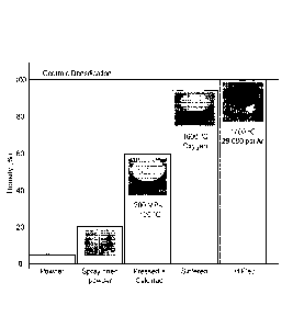
[0077] FIG. 3 provides a chart illustrating exemplary processing steps
(such as those
described above in FIG. 2) for forming an optically transparent, ceramic
garnet
scintillator, as well as the density of the scintillator at the various stages
of manufacture.
- 24 -
CA 03016071 2018-08-28
WO 2017/156143 PCT/US2017/021384
100781 Experimental Results and Comparatil e Examples
100791 Several illustrative experimental results and comparative examples
associated
with the ceramic garnet scintillators described herein are provided below, as
well as methods
of making the same. It is important to note that these experimental results
and comparative
examples are in no way limiting, and are provided for illustration purposes
only.
[0080] Six GYGAG(Ce) ceramic scintillator samples (Samples A-F) were
fabricated
using a single batch of GYGAG(Ce) nanopowder. The six GYGAG(Ce) ceramic
scintilla or
samples were prepared in exactly the same way using the processing steps
described in FIG.
2, except for that each sample was subject to different sintering and/or
annealing conditions.
For instance, Samples A-C were each sintered under vacuum, whereas Samples D-F
were
each sintered in pure 02. After sintering, all the samples attained about
equivalent
transparency and appeared similar by eye in room light. One each of the vacuum
and oxygen
sintered samples (i.e., Samples B and E) were then annealed in air at about
1600 C, and one
each of the vacuum and oxygen sintered samples (i.e., Samples C and F) were
then annealed
under vacuum at about 1600 C. For clarity the sintering/annealing steps
performed for each
sample may be noted as follows, where "vac" is "vacuum":
Sample A: Vac/None
Sample B: Vac/Air
Sample C: Vac/Vac
Sample D: 02/None
Sample E: 02/Air
Sample F: 02/Vac.
-25 -
CA 03016071 2018-08-28
WO 2017/156143 PCT/US2017/021384
10081] To observe the presence of afterglow, Samples A-F were briefly
illuminated with
a 254 nm mercury lamp and photographed in the dark about 1 second after
turning off the
ultraviolet lamp. It was surprisingly and unexpectedly found that that the air-
annealed
samples (i.e., Samples B and E) did not exhibit afterglow, whereas the vacuum
anneal
increased afterglow for the vacuum sintered sample (i.e., Sample C) and
decreased afterglow
for the oxygen sintered sample (i.e., Sample F). The samples that were not
annealed (i.e.,
Samples A and D) each exhibited afterglow.
100821 The rise times and the coincident timing resolution of Samples A-F
was also
measured, and is summarized in Table 1, below. It was also surprisingly and
unexpectedly
found that the air-annealed samples (i.e., Samples B and E) exhibited rise
times and
coincident timing resolution suitable for use in PET scanners, for which <400
ps is likely
required, <300 ps is preferable, and <250 ps is most preferable.
Sample A
(Vac/None) (Vac/Air) (Vac/Vac) (02/None) (02/Air) (02/Vac)
Rise time 8.8 8.4 9.4 14.7 5 11.2
(ns)
Timing 505 333 486 500 240 360
resolution
(ps)
Table 1
100831 FIG. 4 illustrates the decay traces for Samples A-F acquired with Cs-
137 gamma
excitation. It was again surprisingly and unexpectedly found that the
reduction in afterglow
in Samples A-F strongly correlated with shorter decays on the micro-second
timescale, as
shown in Fig. 4. The decays consist of several components: a fast component
with a decay of
about 100 ns and which is assigned to the Ce3+ decay; a medium component with
a decay of
about 500 ns and which is assigned to energy migration via the Ge sublaftice;
and a slow
-26-
CA 03016071 2018-08-28
WO 2017/156143 PCT/US2017/021384
component with a decay of about 1-5 s, thought to be due to shallow traps
that can be
accessed via hopping of carriers to and from the conduction band. It is of
note that this third
component is missing from the decays acquired for the air annealed samples.
The fastest
decays correspond to the air-annealed samples (i.e., Samples B and F),
however, the best
energy resolution of the photopeak is obtained for the vacuum sintered samples
with either
no anneal (i.e., Sample A) or a vacuum anneal (i.e., Sample C). In other
words, the oxygen-
sinter and air-anneal treatments were found to improve the time-resolution at
the "cost" of
degraded energy resolution (for which lower values are better), which renders
the
scintillators fabricated in this manner more suitable for use in PET scanners
rather than for
spectroscopic identification of radioactive isotopes.
[00841 FIG. 5 is the UV absorption spectrum of Samples A-F. The feature in
the UV
absorption spectrum near 300 nm is known to be due to the Ce4- ions, and
therefore serves as
a measure of its content in the samples. It was again surprisingly and
unexpectedly found that
most significant Ce4 absorbance was observed for the air-annealed samples
(i.e., Samples B
and F), with a noticeable enhancement for the 02-sintered samples (i.e.,
Samples D-F).
[00851 All of the above features mentioned in relation to FIGS. 4 and 5
(e.g., observance
of afterglow, observance of Ce' absorbance, effective decay (defined as the
time to 1% of
initial intensity), and resolution obtained at 662 keV) is summarized in Table
2 below.
- 27 -
CA 03016071 2018-08-28
WO 2017/156143
PCT/US2017/021384
Sample A
( Vac/None) (Vac/Air) (Vac/Vac) (02/None) (02/Air) (02/Vac)
Afterglow High Low High High Low Medium
observed?
Ce4+ None High None Low High Low
observed?
Effective 0.74 0.76 0.60 1.2 0.49 1.5
decay ( s)
Resolution 5.4 8.6 5.2 6.0 7.5 6.4
(%)
Table 2
100861 Applications and Uses
[0087] Embodiments of the present invention may be used in a wide variety
of
applications, and potentially any application in which detection of gamma
rays, x-rays,
charged particles, etc. is useful.
[0088] Illustrative uses of various embodiments of the present invention
include, but
are not limited to, applications requiring radiation detection. Medical
imaging
applications, including positron emission tomography (PET), time of flight
(TOF) PET;
Computed Tomography (CT) and other X-ray imaging techniques, combined PET/CT
techniques SPECT, SPEC/CT, etc., are a few such examples.
[0089] For applications pertaining to radiation detection, such as those
discussed
directly above, any of the scintillators described herein may be employed in a
radiation
detector. In particular approaches, this radiation detector may include a
means of reading-
of detecting the light response of the scintillator and registering the
magnitude of the light
yield by employing a photomultiplier tube, silicon photomultiplier,
photodiode, or any
transducer configured to respond to the scintillation light. This radiation
detector may
ultimately produce a pulse height spectrum, where the light response is
presented as a
histogram of the number of counts collected within each bin of light yield
generated by
-28-
CA 03016071 2018-08-28
WO 2017/156143
PCT/US2017/021384
the scintillator. Moreover, in preferred approaches, such a radiation detector
is configured
to register x-rays and/or gamma rays, and is also configured to partially or
completely
distinguish between these particular forms of radiation and approximately
determine the
energy of the gamma or x-ray photon.
[0090] The inventive concepts disclosed herein have been presented by way
of
example to illustrate the myriad features thereof in a plurality of
illustrative scenarios,
embodiments, and/or implementations. It should be appreciated that the
concepts generally
disclosed are to be considered as modular, and may be implemented in any
combination,
permutation, or synthesis thereof. In addition, any modification, alteration,
or equivalent
of the presently disclosed features, functions, and concepts that would be
appreciated by a
person having ordinary skill in the art upon reading the instant descriptions
should also be
considered within the scope of this disclosure.
[0091] While various embodiments have been described above, it should be
understood that they have been presented by way of example only, and not
limitation.
Thus, the breadth and scope of a preferred embodiment should not be limited by
any of
the above-described exemplary embodiments, but should be defined only in
accordance
with the following claims and their equivalents.
-29-