Note: Descriptions are shown in the official language in which they were submitted.
- 1 -
DEVICE, SYSTEM, AND METHOD FOR MEASURING INTERNAL
IMPEDANCE OF A TEST BATTERY USING FREQUENCY RESPONSE
10
20
FIELD
Embodiments of the present disclosure relate to apparatuses, systems, and
methods
for impedance measurement of energy storage cells, such as electrochemical
cells, and
more particularly, to analysis of the state of health of energy storage cells.
BACKGROUND
Chemical changes to electrodes in a rechargeable battery may cause degradation
in
the battery's capacity, duration of charge retention, charging time, and other
functional
parameters. Battery degradation may accumulate over the life of the battery.
Environmental factors (e.g., high temperature) and functional factors (e.g.,
improper
charging and discharging) may accelerate battery degradation. Operators of
systems that
CA 3016537 2019-11-27
CA 03016537 2018-08-31
WO 2017/151955
PCT/US2017/020499
- 2 -
rely on rechargeable battery power may desire to monitor the degradation of
the batteries
they use. One indicator of battery degradation is an increase in battery
impedance.
FIG. 1 is an impedance plot 102 of a fresh battery and an impedance plot 104
of an
aged battery, measured at several different frequencies using an
Electrochemical
Impedance Measurement (EIM) system. The Y-axis is the imaginary impedance and
the
X-axis is the real impedance for a plurality of different frequencies plotted
in FIG. I. As
illustrated in FIG. 1, the aged battery (plot 104) exhibits a higher impedance
than the fresh
battery (plot 102) at each of the different frequencies. Operators of systems
that rely on
rechargeable batteries may use impedance data, such as the impedance data of
FIG. 1, to
determine that a replacement battery is needed before a failure occurs. Such
preemptive
replacement may prevent expensive delays and property damage that may occur in
the
event of a battery failure. Also, knowledge of a battery's continued
reliability may prevent
expenses associated with unnecessarily replacing a battery that still has a
substantial
amount of lifetime left.
Existing impedance measurement systems have a resolution of approximately 0.1
mOhm when operating at an excitation current range of approximately 500 mA. As
a
result, existing impedance measurement systems may be able to determine the
impedance
of a test battery exhibiting a 10 mOhm internal impedance with adequate
resolution. The
resolution of existing impedance measurement systems may limit the ability to
test
batteries exhibiting lower internal impedance (e.g., 1 mOhm). Other methods of
impedance measurement (e.g., electro-chemical impedance spectroscopy) may
achieve
high resolution, but may be slow to be tuned, such as requiring time on the
order of about
10 minutes to obtain the measurements.
DISCLOSURE
Disclosed herein is an impedance measurement device. The impedance
measurement device comprises a current driver configured to generate an
excitation current
signal to be applied to a test battery responsive to a control signal, and a
processor operably
coupled with the current driver. The processor is configured to generate the
control signal
during an auto-ranging mode and a measuring mode. The auto-ranging mode
applies the
excitation current signal to the test battery over a plurality of different
amplitudes to
measure a response to the excitation current signal at each amplitude. The
measuring mode
CA 03016537 2018-08-31
WO 2017/151955 PCT/US2017/020499
- 3 -
applies the excitation current signal to the test battery for an amplitude
responsive to the
results of the auto-ranging mode.
In some embodiments, an impedance measurement system is disclosed. The
impedance measurement system includes a test battery and an impedance
measurement
device operably coupled to the test battery. The impedance measurement device
includes a
preamplifier including a current driver and a signal measuring module operably
coupled
with the test battery, a current control signal generator operably coupled
with the
preamplifier, a data acquisition system operably coupled with the
preamplifier, and a
processor operably coupled with the current control signal generator and the
data
acquisition system. The processor is configured to control the current control
signal
generator to transmit a current control signal to the preamplifier during an
auto-ranging
mode to cause the current driver to generate an excitation current signal
exhibiting a range
of amplitudes, control the data acquisition system to analyze the response of
the test battery
from the signal measuring module during the auto-ranging mode, control the
current
control signal generator to transmit the current control signal to the
preamplifier during a
measuring to cause the current driver to generate the excitation current
signal exhibiting an
selected amplitude based, at least in part, on analyzing the response of the
test battery
during the auto-ranging mode, and control the data acquisition system to
analyze the
response of the test battery from the signal measuring module during the
measuring mode
to determine an impedance of the test battery.
In some embodiments, a method of measuring impedance of a test battery is
disclosed. The method comprises applying an excitation current signal to a
test battery
including a plurality of pulses exhibiting different amplitudes during an auto-
ranging mode,
measuring an electrical signal from the test battery responsive to the
excitation current
signal over the plurality of different amplitudes, applying the excitation
current signal to
the test battery exhibiting a fixed amplitude during a measuring mode, wherein
the fixed
amplitude is set based, at least in part, on an analysis of the electrical
signal measured
during the auto-ranging mode, and measuring the electrical signal from the
test battery
responsive to the excitation current signal exhibiting the fixed amplitude
during the
measuring mode to determine an internal impedance of the test battery.
CA 03016537 2018-08-31
WO 2017/151955 PCT/US2017/020499
- 4 -
BRIEF DESCRIPTION OF THE DRAWINGS
FIG. 1 is an impedance plot of a fresh battery and an impedance plot of an
aged
battery, measured at several different frequencies using an Electrochemical
Impedance
Measurement System.
FIG. 2 is a simplified block diagram of an impedance measurement system
configured to perform real-time impedance spectrum measurement of a test
battery
according to an embodiment of the present disclosure.
FIG. 3 is a simplified block diagram of selected features of the impedance
measurement device of the impedance measurement system of FIG. 2.
FIG. 4 is a simplified block diagram of the current driver of FIG. 3.
FIG. 5 illustrates a circuit diagram of the signal measuring module of the
preamplifier of FIGS. 2 and 3.
FIG. 6 is a flowchart illustrating a method for operating an impedance
measurement
system of a battery according to an embodiment of the present disclosure.
MODE(S) FOR CARRYING OUT THE INVENTION
In the following detailed description, reference is made to the accompanying
drawings, which form a part hereof, and in which is shown by way of
illustration specific
embodiments in which the present disclosure may be practiced. These
embodiments are
described in sufficient detail to enable those of ordinary skill in the art to
practice the present
disclosure. It should be understood, however, that the detailed description
and the specific
examples, while indicating examples of embodiments of the present disclosure,
are given by
way of illustration only and not by way of limitation. From this disclosure,
various
substitutions, modifications, additions rearrangements, or combinations
thereof within the
scope of the present disclosure may be made and will become apparent to those
of ordinary
skill in the art.
In accordance with common practice, the various features illustrated in the
drawings
may not be drawn to scale. The illustrations presented herein are not meant to
be actual views
of any particular apparatus (e.g., device, system, etc.) or method, but are
merely idealized
representations that are employed to describe various embodiments of the
present disclosure.
Accordingly, the dimensions of the various features may be arbitrarily
expanded or reduced
for clarity. In addition, some of the drawings may be simplified for clarity.
Thus, the
CA 03016537 2018-08-31
WO 2017/151955 PCT/US2017/020499
- 5 -
drawings may not depict all of the components of a given apparatus or all
operations of a
particular method.
Information and signals described herein may be represented using any of a
variety of
different technologies and techniques. For example, data, instructions,
commands,
information, signals, bits, symbols, and chips that may be referenced
throughout the
description may be represented by voltages, currents, electromagnetic waves,
magnetic fields
or particles, optical fields or particles, or any combination thereof Some
drawings may
illustrate signals as a single signal for clarity of presentation and
description. It should be
understood by a person of ordinary skill in the art that the signal may
represent a bus of
signals, wherein the bus may have a variety of bit widths and the present
disclosure may be
implemented on any number of data signals including a single data signal.
The various illustrative logical blocks, modules, circuits, and algorithm acts
described
in connection with embodiments disclosed herein may be implemented as
electronic
hardware, computer software, or combinations of both. To clearly illustrate
this
interchangeability of hardware and software, various illustrative components,
blocks,
modules, circuits, and acts are described generally in terms of their
functionality. Whether
such functionality is implemented as hardware or software depends upon the
particular
application and design constraints imposed on the overall system. Skilled
artisans may
implement the described functionality in varying ways for each particular
application, but
such implementation decisions should not be interpreted as causing a departure
from the scope
of the embodiments of the disclosure described herein.
In addition, it is noted that the embodiments may be described in terms of a
process
that is depicted as a flowchart, a flow diagram, a structure diagram, or a
block diagram.
Although a flowchart may describe operational acts as a sequential process,
many of these
acts can be performed in another sequence, in parallel, or substantially
concurrently. In
addition, the order of the acts may be rearranged. A process may correspond to
a method, a
function, a procedure, a subroutine, a subprogram, etc. Furthermore, the
methods disclosed
herein may be implemented in hardware, software, or both. If implemented in
software, the
functions may be stored or transmitted as one or more computer-readable
instructions (e.g.,
software code) on a computer-readable medium. Computer-readable media may
include both
computer storage media and communication media including any medium that
facilitates
transfer of a computer program from one place to another. Computer-readable
media may
include volatile and non-volatile memory, such as, for example, magnetic and
optical storage
CA 03016537 2018-08-31
WO 2017/151955 PCT/US2017/020499
- 6 -
devices. such as, for example, hard drives, disk drives, magnetic tapes, CDs
(compact discs),
DVDs (digital versatile discs or digital video discs), solid state storage
devices (solid state
drives), and other similar storage devices.
It should be understood that any reference to an element herein using a
designation
such as "first," "second," and so forth does not limit the quantity or order
of those elements,
unless such limitation is explicitly stated. Rather, these designations may be
used herein as a
convenient method of distinguishing between two or more elements or instances
of an
element. Thus, a reference to first and second elements does not mean that
only two elements
may be employed there or that the first element must precede the second
element in some
manner. Also, unless stated otherwise a set of elements may comprise one or
more elements.
When describing circuit elements, such as, for example, resistors, capacitors,
and transistors,
designators for the circuit elements begin with an element type designator
(e.g., R, C, M)
followed by a numeric indicator.
As used herein, the terms "energy storage cell" and "energy storage cells"
refer to
rechargeable electrochemical cells that convert chemical energy to a direct
current electrical
voltage potential across a positive terminal and a negative terminal of the
energy storage cell.
The terms "battery,- "cell,- and "battery cell- may each be used
interchangeably herein with
the term "energy storage cell."
As used herein, the term "mid-range voltage" means a voltage in a range near
50 V.
Thus, a mid-range voltage may include an average voltage of about 40 V to 60 V
with a
variation of about 90% to 99% depending on the tolerances desired for a given
system.
As used herein, the term "high-range voltage- means a voltage in a range near
300 V. Thus, a high-range voltage may include an average voltage of about 250
V to
350 V with a variation of about 90% to 99% depending on the tolerances desired
for a
given system.
As used herein, the terms "sinusoid,- and "sinusoidal," refer to electrical
signals (e.g.,
currents and voltage potentials) that oscillate at least substantially
according to a sine or cosine
function (e.g., having various magnitudes and phase shifts) over time As
should be readily
apparent to those of ordinary skill in the art, any given sinusoidal signal
may be equivalently
expressed either as a sine function or a cosine function, as the sine and
cosine are merely
phase-shifted versions of each other. Sinusoidal signals are disclosed herein
as being applied
to energy storage cells and shunts (e.g., resistors of known resistance values
for calibration
purposes). In some cases, these sinusoidal signals are referred to more
specifically herein as
CA 03016537 2018-08-31
WO 2017/151955 PCT/US2017/020499
- 7 -
either sine signals or cosine signals. These specific references to sine
signals and cosine
signals may be indicative of the phase of such signals relative to a time when
a sinusoidal
signal is first asserted to a conductive line (e.g., a positive or negative
battery terminal, a
conductive trace on a circuit board, a wire, etc.).
As used herein, the term "sum-of-sinusoids" ("SOS") refers to electrical
signals that
oscillate according to a sum of sinusoidal signals. An SOS signal may include
sums of sine
signals, sums of cosine signals, or combinations thereof For example, a
harmonic orthogonal
synchronous transform (HOST) SOS signal may include a base sinusoidal signal
having a
base frequency summed with one or more sinusoidal signals having successive
integer
harmonic frequencies of the base frequency, and alternating between sine
signals and cosine
signals (or some phase-shifted version thereof) for each successive harmonic.
The orthogonal
nature of the harmonic sinusoidal signals summed together in a HOST SOS may
serve to
reduce or eliminate excessive transients. While examples are provided herein
referring to
SOS signals, embodiments of the present disclosure also contemplate using
other types of
excitation signals, including sum of alternating sines, cosines (ASC) signals.
FIG. 2 is a simplified block diagram of an impedance measurement system 200
configured to perform real-time impedance spectrum measurement of a test
battery 205
according to an embodiment of the present disclosure. The test battery 205
refers to the
battery under test, and may be an actual battery deployed and in use by an end
user. The
impedance measurement system 200 may include an impedance measurement device
(IMD) 210 (sometimes referred to as an impedance measurement box (IMB))
operably
coupled to the test battery 205. The IMD 210 may include a processor 212, a
data
acquisition system (DAS) 214, an SOS generator (SOSG) 216, a preamplifier 218,
and a
power supply 222. The IMD 210 may be used in a variety of different
environments and
battery types such that the health of the battery may be monitored in situ. As
an example,
the impedance measurement system 200 may be incorporated within an automobile
or
other vehicle with batteries that include one or more energy storage cells.
Such vehicles
may include electric or hybrid vehicles. It is also contemplated that
embodiments of the
disclosure may be employed in non-vehicular applications such as, by way of
non-limiting
example, in association with energy storage cells operably coupled to solar,
wind, or tidal
energy generation systems.
The SOSG 216 may be configured to generate an SOS control signal to the
preamplifier 218 to control an SOS current signal output by the preamplifier
218. The SOS
CA 03016537 2018-08-31
WO 2017/151955 PCT/US2017/020499
- 8 -
control signal may be selected to cause the preamplifier 218 to provide an SOS
current signal
including a sum of a plurality of different current signals having a plurality
of different
frequencies of interest for testing impedance of the test battery 205. In some
embodiments,
the SOS control signal may include a voltage signal proportional to a desired
current for the
SOS current signal to be output by the preamplifier 218. Accordingly, the SOS
control signal
may include an SOS voltage signal. An SOS signal is used herein as an example,
and the
SOSG 216 may be an excitation current control signal generator that is
configured to control
other types of excitation current signals to apply to the test battery 205.
Thus, SOS signals are
used herein as a non-limiting example of a signal that may be applied to the
test battery 205.
The IMD 210 may be configured to measure electrical signals 206 at terminals
of the
test battery 205 responsive to the SOS current signal being applied to the
terminals of the test
battery 205. The preamplifier 218 may be configured to measure a battery
response signal
(e.g., voltage response and/or current response) responsive to receiving the
electrical
signals 206 from the test battery 205. The DAS 214 may be configured to
receive the battery
response signal and compute the impedance of the test battery 205 at the
frequencies of the
SOS control signal. In this way, the IMD 210 may be configured to test the
impedance of the
test battery 205 at a plurality of different frequencies substantially
simultaneously.
In some embodiments, the DAS 214 may divide the measured voltage response by
the
measured current response to obtain the impedance response of the test battery
205. In such
embodiments, no calibration may be needed because the impedance of the test
battery 205
may be determined by dividing a measured voltage by a measured current. In
some
embodiments, the DAS 214 may be configured to measure only a voltage response
of the test
battery 205 to the SOS current signal 356 (FIG. 3). In such embodiments,
calibration may be
needed to determine the impedance of the test battery 205. Different
calibration methods
(e.g., single-shunt calibration, multiple shunt calibration, etc.) are
contemplated, which may
be used to account for real and imaginary portions of signals. For a single
shunt method, a
standard deviation may be determined for its measurements over time, and then
an unknown
shunt resistance may be determined by equating a ratio of the known single
shunt resistance to
the standard deviation of the measurements over its time record.
The IMD 210 may utilize data processing methods (e.g., algorithms) for
generating
battery impedance spectrum data 225. Impedance spectrum data 225 may be
transmitted
from the IMD 210 to a remote computer 230. The impedance spectrum data 225 may
be
formatted in any suitable format (e.g., Comma Separated Values (CSV) format).
Each
CA 03016537 2018-08-31
WO 2017/151955 PCT/US2017/020499
- 9 -
individual spectrum may include a time stamp, an information header, and the
impedance
spectrum data 225 may include the frequencies, the real part of the impedance,
the
imaginary part of the impedance and the common mode battery voltage for that
spectrum.
Additional data that may be transmitted to the remote computer 230 with the
impedance
spectrum data 225 include the SOS RMS current and the magnitude and phase
calibration
constants. The remote computer 230 may include a personal computer, a tablet
computer,
a laptop computer, a smart phone, a server, a vehicle computer (e.g., central
processing
unit), or other suitable computing devices.
A user may control the IMD 210 from the remote computer 230 using
commands 235 via an interface, such as a Universal Serial Bus (USB) interface,
hardwire
serial interfaces, hardwire parallel interfaces, a wireless interfaces (e.g.,
WiFi, ZIGBEE ,
BLUETOOTHR), or other suitable interface. For example, the IMD 210 may be able
to be
controlled via a human interface on the remote computer 230 or the IMD 210 for
the
purpose of inputting control constraints to the IMD 210, performing embedded
system
diagnostics, calibration, or performing manual impedance spectrum acquisition.
The
IMD 210 may implement a minimum of three-point magnitude and phase calibration
for
each frequency within the SOS control signal.
The processor 212 may be configured to synchronize and control the DAS 214,
the
SOSG 216, and the preamplifier 218. In some embodiments, the measurements may
be
performed according to a set schedule and/or control parameters dictated by
the remote
computer 230. As a non-limiting example, the processor 212 may interface with
the
remote computer 230 to download desired parameters and commands and upload
various
measured data. As non-limiting examples, the processor 212, or other devices
not shown
such as memory, may include adequate buffer memory to hold an acquired battery
response
time record until processed, hold the desired number of battery impedance
spectrums for
archive, hold system control and interface software, hold high resolution SOS
samples, and
hold the impedance spectrum control parameters. The processor 212 may be
further
configured to accept downloaded impedance spectrum control and calibration
parameters
and upload to the remote computer 230 archived battery impedance spectrum data
under
direction of the remote computer 230.
In operation, when a measurement is executed, the DAS 214 may transmit a
digital
signal ("Power Up") to the power supply 222 to cause the power supply 222 to
power up
the rest of the system (e.g., the preamplifier 218). The electrical signals
206 may be
CA 03016537 2018-08-31
WO 2017/151955 PCT/US2017/020499
- 10 -
measured by the in the preamplifier 218 and input to the DAS 214 as the analog
signal
"Battery Voltage." At least one of the DAS 214 or the processor 212 may
digitize the
voltage and may send the digitized result to the remote computer 230. At least
one of the
remote computer 230 or the processor 212 may then process the measured DC
battery
voltage and use the DAS 214 to send a series of digital signals (e.g., "Buck
Signals", "Buck
DiA Control," etc.) to the preamplifier 218 to generate a DC bias voltage to
subtract from
the DC voltage response from the overall response of the test battery 205. As
will be
discussed further below with reference to FIG. 5, a low buck signal and a high
buck signal
may be generated to achieve the higher gain signals used for improved
measurement
resolution.
With the preamplifier 218 connected to the test battery 205, at least one of
the
remote computer 230 or processor 212 sends a measurement signal such as, for
example,
the SOS control signal or other suitable measurement signal to the
preamplifier 218. When
the test battery 205 is excited with the SOS current, the voltage that appears
at its terminals
may be the battery voltage plus any voltage drop of the SOS current acting on
the internal
impedance of the test battery 205. It is this SOS voltage drop that, when
captured and
processed, will yield the spectrum of the battery impedance for the test
battery- 205. A
challenge may be that the battery voltage can be as much as two orders of
magnitude
greater than the SOS voltage drop. Thus, to accurately detect that signal, the
battery
voltage may be subtracted out prior to measuring the SOS voltage drop allowing
all the bits
of resolution of the AID convertor to focus on the desired signal to greatly
improve
accuracy. This subtraction of the battery voltage may be accomplished by
measuring the
battery voltage prior to the application of the SOS current and then feeding
back a
computer generated buck voltage that is subtracted with a differential
amplifier from the
total battery voltage to yield only the SOS voltage.
In one embodiment, the SOSG 216, under control of the processor 212, may be
configured to synthesize a sample clock to be used by the DAS 214. The sample
clock
frequency may be selected at a rate that may differ depending on the data
processing
method used. The SOSG 216 may have a programmable signal level for the DAC
output
to the smoothing filter 306 (FIG. 3), which enables the processor 212 to
control the SOS
RMS current level to the test battery 205. The SOSG 216, under the control of
the
processor 212, may be configured to operate in an auto-ranging mode as well as
a
measuring mode. The auto-ranging mode may occur prior to the measuring mode to
CA 03016537 2018-08-31
WO 2017/151955 PCT/US2017/020499
- 11 -
determine the SOS current amplitude that should be used for the SOS current
during the
measuring mode. The auto-ranging mode and the measuring mode will be discussed
further below with respect to FIG. 6.
The DAS 214 may be configured with a desired resolution (e.g., 16 bit, 32 bit,
etc.)
and accept an external sample clock from the SOSG 216 with clock frequency
that may
range, for example, from 1 kHz to 100 kHz. The DAS 214 may accept an enable
signal
from the processor 212 to start acquiring data concurrent with the application
of the SOS
current signal to the test battery 205 being tested during its auto-ranging
mode or its
measuring mode. The DAS 214 may accept the analog battery voltage signal that
has been
conditioned by the preamplifier 218 for digitizing. The DAS 214 may include a
buffer
memory to hold a sample of the digitized battery voltage signal for uploading
to memory
(not shown). Each of the acquired samples may become part of the time record
array that is
input into the data processing method. Additionally, the DAS 214 may acquire a
measurement of the DC voltage and case temperature of the test battery 205
prior to the
application of the SOS current.
In some embodiments, the SOS current leads may be configured as a twisted pair
and protected with a fuse. The preamplifier 218 may utilize a full
differential battery
voltage sense and may incorporate a method to bias out the common mode battery
voltage
from the batteries response to the SOS current excitation. This biasing may
enable the full
resolution of the DAS 214 to be focused upon the test batteries response to
the SOS current
rather than the average battery voltage.
The preamplifier 218 input signal may be the zero order hold SOS control
signal
from the SOSG 216. The preamplifier 218 may include an active Butterworth low-
pass
filter as the smoothing filter 306 (FIG. 3) and include about 1 dB of
attenuation at 8 kHz
and 60 dB of attenuation to the frequencies introduced by the zero order hold
upon the SOS
signal. The SOS control signal may then be fed into a current driver 308 (FIG.
3), which
converts the SOS control signal into a current (e.g., "SOS Current") provided
to the test
battery 205. A signal measuring module 310 (FIG. 3) of the preamplifier 218
may detect
the battery voltage and subtract a DC buck voltage to become the battery
response that may
be digitized by the DAS 214. The resultant battery response may be used by
various data
processing methods discussed herein to generate the impedance spectrum.
In some embodiments, an optional connection circuit (not shown) may be
included
between the preamplifier 218 and the test battery 205 to isolate at least one
signal line of the
- 12 -
preamplifier 218 providing the SOS current signal from a direct current
voltage sourced by the
test battery 205. As a result, sensitive electronics included in the
preamplifier 218 may not be
exposed to the extremes of the direct current voltage potential sourced by the
test battery 205.
Also, the preamplifier 218 may be subjected to less noise than if the analog
ground were
extended outside of the preamplifier 218. As a result, the connection to the
test battery 205
may be disconnected when the SOS current signal is not being sent to the test
battery 205. An
example of such an optional connection circuit that uses relays coupled to
between the
preamplifier 218 and the test battery 205 is described in United States Patent
Application
Publication No. 2014/0358462, filed June 4, 2014, entitled "Apparatuses and
Methods for
Testing Electrochemical Cells by Measuring Frequency Response."
FIG. 3 is a simplified block diagram of selected features of the IMD 210 of
the
impedance measurement system 200 of FIG. 2. As shown in FIG. 3, the IMD 210
may
include an SOS control module 302, a digital-to-analog converter (DAC) 304, a
smoothing
filter 306, a signal measuring module 310, and an impedance computation module
312. The
SOSG 216 may incorporate the SOS control module 302 and the DAC 304. The
preamplifier 218 may incorporate the smoothing filter 306, the current driver
308, and the
signal measuring module 310. The DAS 214 may incorporate the impedance
computation
module 312.
The SOS control module 302 may be configured to generate a digital SOS signal
350
including a sum of sinusoids having a plurality of different frequencies that
are of interest for
impedance measurement of the test battery 205 (FIG. 2). The digital SOS signal
350 may be
sampled at least at a Nyquist rate of a highest one of the plurality of
different frequencies of
the digital SOS signal 350. The digital SOS signal 350 may also represent at
least one period
of a lowest one of the plurality of different frequencies of the digital SOS
signal 350. The
SOS control module 302 may be configured to provide the digital SOS signal 350
to the
DAC 304.
The DAC 304 may be configured to convert the digital SOS signal 350 to an
analog
signal transmitted to the preamplifier 318. As those of ordinary skill in the
art should
understand, digital signals, such as the digital SOS signal 350, are only
capable of manifesting
a discrete set of discontinuous signal levels. As a result, when digital
signals are converted to
analog signals, the analog equivalent may manifest stepwise, or "choppy,"
fluctuations. Thus,
the analog signal generated by the DAC 304 may be a choppy SOS signal 352 that
manifests
CA 3016537 2019-11-27
CA 03016537 2018-08-31
WO 2017/151955 PCT/US2017/020499
- 13 -
stepwise fluctuations. This choppy SOS signal 352 may be received by the
smoothing
filter 306 within the preamplifier 218. In some embodiments, the smoothing
filter 306 may be
incorporated within the SOSG 216.
The smoothing filter 306 may be configured to "smooth" the choppy SOS signal
352
to provide a smooth SOS control signal 354. By way of non-limiting example,
the smoothing
filter 306 may include a low-pass filter configured to smooth the stepwise
fluctuations of the
choppy SOS signal 352. The smooth SOS control signal 354 may be provided to
the current
driver 308. Responsive to the smooth SOS control signal 354 being provided to
the current
driver 308, the current driver 308 may transmit a corresponding SOS current
signal (FIG. 2) to
the test battery 205.
As should be appreciated by those of ordinary skill in the art, a filter may
alter a
magnitude, phase, or combination thereof, of periodic signals. It should also
be appreciated
that filters may alter the magnitude and phase of different components of
signals oscillating at
different frequencies in different ways. Accordingly, each of the different
frequency
components of the smooth SOS control signal 354 may be altered in magnitude,
frequency, or
a combination thereof, from the corresponding magnitude and frequency of the
different
frequency components of the digital SOS signal 350, due at least in part to
the smoothing
filter 306.
In some embodiments, properties of the smoothing filter 306 may be known to
analytically estimate the frequency response of smoothing filter 306. In some
embodiments,
calibration may be used to determine the frequency response to the smoothing
filter 306. The
SOS control module 302 may use the frequency response of the smoothing filter
306 to take
into account expected changes in magnitude, phase, or a combination thereof,
that the
smoothing filter 306 is expected to impose on the different frequency
components of the SOS
control signal 354. The SOS control module 302 may compensate for the expected
changes
when generating the digital SOS signal 350. In other words, the SOS control
module 302 may
be configured to pre-emphasize the digital SOS signal 350 to compensate for
the response of
the smoothing filter 306. By way of non-limiting example, if the smoothing
filter 306 is
expected to attenuate and shift a first frequency component of the choppy SOS
signal 352 by
known amounts, the SOS control module 302 may preemptively increase the
magnitude and
shift the phase of the corresponding first frequency component of the digital
SOS signal 350
by the known amounts to compensate for the expected changes.
CA 03016537 2018-08-31
WO 2017/151955 PCT/US2017/020499
- 14 -
The signal measuring module 310 may be configured to measure electrical
signals 206
at the terminals of the test battery 205. By way of non-limiting example, the
signal measuring
module 310 may be configured to measure a voltage response of the test battery
205 to the
SOS signal, a current response of the test battery 205 to the SOS signal, or a
combination
thereof The signal measuring module 310 may be configured to provide the
impedance
computation module 312 with measured signal data 360 indicating the measured
response of
the test battery 205 to the SOS signal.
The impedance computation module 312 may be configured to compute a determined
impedance (impedance data 362) of the test battery 205 using the measured
signal data 360
from the signal measuring module 310. By way of non-limiting example, the
measured signal
data 360 may include both the voltage response and the current response of the
test
battery 205 to the SOS current signal 356 (FIG. 2). The impedance computation
module 312
may be configured to divide the voltage response by the current response for
each of the
plurality of different frequencies of the SOS current signal 356 to determine
the impedance
data 362 for each of the plurality of different frequencies.
Also by way of non-limiting example, the measured signal data 360 may include
only
the voltage response of the test battery 205 to the SOS current signal 356.
The impedance
computation module 312 may be configured to estimate the current response
using the voltage
response and calibration data from previous or subsequent calibrations of the
control circuitry.
A known calibration response may be measured by applying the SOS current
signal 356 to
one or more shunts of known impedance, and measuring and storing calibration
data including
the response of the one or more shunts to the SOS current signal 356.
The impedance computation module 312 may be configured to provide or store
impedance data 362 including the determined impedance of the test battery 205
at each of the
frequencies included in the digital SOS signal 350 (i.e., the same frequencies
included in the
choppy SOS signal 352, the SOS control signal 354, and the SOS current signal
356). In
some embodiments, the impedance data 362 may be displayed to a user of the
impedance
measurement system 200 (FIG. 2) (e.g., on an electronic display of the
impedance
measurement system 200 in list form, in plot form, in table form, etc.). In
some embodiments,
the impedance data 362 may be processed automatically to determine whether the
test
battery 205 should be replaced, and the user may be informed of the automatic
determination.
In some embodiments, the impedance data 362 may be processed automatically to
determine
an estimate of how much life is remaining to the test battery 205. Such
automatic processing
CA 03016537 2018-08-31
WO 2017/151955 PCT/US2017/020499
- 15 -
may be performed locally by the impedance measurement system 200, remotely by
a
computing device (e.g., remote computer 230) configured to communicate with
the
impedance measurement system 200, or combinations thereof A warning (e.g.,
visual,
audible, or a combination thereof) may be provided when the IMD 210 detects
that the test
battery 205 should be replaced.
FIG. 4 is a simplified block diagram of the current driver 308 of FIG. 3. In
some
embodiments, the current driver 308 may include differential current sources
including a push
current source 410 and a pull current source 420 that are configured to
receive the SOS
control signal 354 (e.g., through the smoothing filter 306 (FIG. 3)) and
generate the SOS
current signal 356 provided to the test battery 205. The SOS current signal
356 may include a
current signal that is proportional to a voltage potential of the SOS control
signal 354. As
discussed above, the SOS current signal 356 may include a sum of sinusoidal
current signals
having frequencies of interest for test battery 205 impedance measurements.
The push current source 410 may be configured to push current 'PUSH into the
test
battery 205, and the pull current source 420 may be configured to pull current
'PULL from the
test battery 205. The analog ground terminal GND of the current driver 308 may
be floated
between the push current source 410 and the pull current source 420, isolating
the analog
ground terminal GND from the terminals of the test battery 205. The push
current source 410
and the pull current source 420 may be high impedance current sources. As a
result, the SOS
current excitation circuitry may be fully high impedance ground isolated. As a
result, the
system analog ground GND may be moved to within the IMD 210 (FIG. 2) where it
is better
shielded from noise than in many conventional systems. In addition, the
current driver
voltages powering the operational amplifiers 412, 422 may be balanced (e.g.,
at + 30V) which
may further reduce noise from the power supply 222 (FIG. 2). As a result of
the balanced
voltages for the current driver 308, a protector may not be necessary for
protecting the current
driver 308 if the test battery 205 is connected backward.
In some embodiments, the push current source 410 may include an operational
amplifier 412 operably coupled to resistors Ri-NTA1, RINA2, R
_FA1, RFA2, and RSA in an operational
amplifier current source configuration. Input resistors R1NA1 and R1NA2 may be
operably
coupled to the inverting input and the non-inverting input, respectively, of
the operational
amplifier 412. The non-inverting input of the operational amplifier 412 may be
configured to
receive the SOS control signal 354 through the resistor RINA2. The inverting
input of the
CA 03016537 2018-08-31
WO 2017/151955 PCT/US2017/020499
- 16 -
operational amplifier 412 may be operably coupled to analog ground GND through
resistor
REsAi. Resistors RINAi and RINA2 may be selected to have the same resistance
value RINA.
The inverting input of the operational amplifier 412 may also be operably
coupled to
an output of the operational amplifier 412 through resistor RFAI. The non-
inverting input of
the operational amplifier 412 may be operably coupled to the output of the
operational
amplifier 412 through resistors RFA2 and RSA. The resistance of RFAI and RFA2
may be
selected to have the same resistance value RFA. An output of the push current
source 410 may
be located between resistors RFA2 and RSA. Accordingly, a push portion of the
SOS current
signal 356 may be provided between resistors RFA2 and RSA. Thus configured,
the push
portion of the SOS current signal 356 provided by the push current source 410
may be
expressed as:
RFA
'PUSH r-SOSCON7'ROL R 1õR
SA
where Ipusti is the current provided by the push current source 410, and
VsoscoNfRoL is
the voltage potential of the SOS control signal 354. As may be seen by
inspecting this
expression, the busit is proportional to VsoscoNTRou
In some embodiments, the pull current source 420 may include an operational
amplifier 422 operably coupled to resistors RE=mi, RINB2, RTBI, Rpm, and RsB
in an operational
amplifier current source configuration. Input resistors R1NB1 and R1B2 may be
operably
coupled to the inverting input and the non-inverting input, respectively, of
the operational
amplifier 422. The inverting input of the operational amplifier 422 may be
configured to
receive the SOS control signal 354 through the resistor RNB1. The non-
inverting input of the
operational amplifier 422 may be operably coupled to analog ground GND through
resistor
RINB2. Resistors RINB1 and RINB2 may be selected to have the same resistance
value RINB.
The inverting input of the operational amplifier 422 may also be operably
coupled to
an output of the operational amplifier 422 through resistor RFBI. The non-
inverting input of
the operational amplifier 412 may be operably coupled to the output of the
operational
amplifier 422 through resistors RFB2 and RsB. The resistance of RFBI and RFB2
may be selected
to have the same resistance value RFB. An output of the pull current source
420 may be
located between resistors RFB2 and RsB. Accordingly, a pull portion 'PULL of
the SOS current
signal 356 may be pulled from by a node between resistors RFB2 and RsB. Thus
configured,
the pull portion 'PULL of the SOS current signal 356 pulled by the pull
current source 420 may
be expressed as:
- 17 -
RFB
'PULL VSOSCONTROL RINBRSB
where 'PULL is the current pulled by the pull current source 420, and
VsoscoNTRoi is the
voltage potential of the SOS control signal 354. As is apparent from
inspection of this
expression. Iptru, is proportional to Vsos CONTROL. Additional details
regarding a configuration
including a push current source and a pull current source are described in
United States Patent
Application No. 14/789,959, filed July 1, 2015, entitled "Apparatuses and
Methods for
Testing Electrochemical Cells by Measuring Frequency Response."
In
some embodiments, the current driver 308 may include a single-ended current
driver in place
of the push-pull current driver of FIG. 4. An example of a single-ended
current driver is
described in United States Patent Application Publication No. 2014/0358462,
filed June 4,
2014, entitled "Apparatuses and Methods for Testing Electrochemical Cells by
Measuring
Frequency Response."
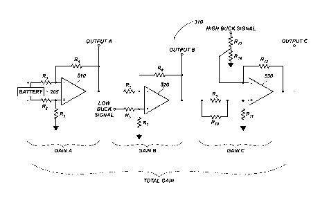
FIG. 5 illustrates a circuit diagram of the signal measuring module 310 of the
preamplifier 218 of FIGS. 2 and 3. The signal measuring module 310 may be
suitable for use
with mid-range voltage systems (e.g., approximately 50 V) as well as high-
range voltage
systems (e.g., approximately 300 V). Other voltage ranges are also
contemplated. The signal
measuring module 310 includes a plurality of operational amplifiers 510, 520,
530 operably
coupled as a first gain stage (operational amplifier 510) and additional gain
stages (operational
amplifiers 520, 530) that cascade from the first gain stage. The first gain
stage exhibits a first
gain (Gain A), the second gain stage exhibits a second gain (Gain B), and the
third gain stage
exhibits a third gain (Gain C).
The test battery 205 may be connected to the first amplifier 510 acting as an
attenuator. As shown in FIG. 5, the positive terminal of the test battery 205
may be coupled to
the inverting input of the first amplifier 510 (e.g., through resistor R1),
and the negative
terminal of the test battery 205 may be coupled to the non-inverting input of
the first
amplifier 510 (e.g., through the voltage divider of resistors R2, R3). The
output of the first
amplifier 510 (i.e., output A) may be returned to the DAS 214 (FIG. 2). The
values of
resistors R1, R2, R3, and R4 may be selected for a desired Gain A. In some
embodiments,
Gain A is approximately -0.166. Thus, the voltage sent to the DAS 214 as
output A may be
CA 3016537 2019-11-27
CA 03016537 2018-08-31
WO 2017/151955 PCT/US2017/020499
- 18 -
within a range of about +/- 10 V for a 50 V battery. For a 300 V battery, the
voltage sent to
the DAS 214 as output A may be within a range of about 60 V.
The second amplifier 520 may be used to condition the battery voltage and set
an
appropriate voltage for comparison to a low buck signal received from the DAS
214. In
particular, the second amplifier 520 may receive the output (i.e., output A)
from the first
amplifier 510 at its inverting input (e.g., through resistor R5), and the buck
signal from the
DAS 214 at its non-inverting input (e.g., through the voltage divider of
resistors R6, R7). The
output of the second amplifier 520 (i.e., output B) may be returned to the DAS
214. The
values of resistors R5, R6, R7, and R8 may be selected for a desired Gain B.
In some
embodiments, Gain B is approximately -20 (e.g., -19.85). Thus, the voltage
sent to the
DAS 214 as output B may be within a range of about +/- 200 V for a 50V battery
(assuming
Gain A is approximately -0.166). For a 300 V battery, the voltage sent to the
DAS 214 as
output B may be within a range of about 1.2 kV (assuming Gain A is
approximately -0.166).
The third amplifier 530 may be used to condition the battery voltage and set
an
appropriate voltage for comparison to a buck signal from the DAS 214. In
particular, the third
amplifier 530 may receive the output (i.e., output B) from the second
amplifier 520 at its
non-inverting input (e.g., through voltage divider of resistors R9/R10, and
R11), and the buck
signal from the DAS 214 at its inverting input (e.g., through the voltage
divider of resistors
R13, R14). The output of the third amplifier 530 (i.e., output C) may be
returned to the
DAS 214. The values of resistors R9, R10, R11, R12, R13, and R14 may be
selected for a
desired Gain C. In some embodiments, Gain C is approximately +20 (e.g.,
+19.95). Thus, the
voltage sent to the DAS 214 as output C may be within a range of about +/- 4kV
for a 50 V
battery (assuming Gain A is approximately -0.166, and Gain B is approximately -
20). For a
300 V battery, the voltage sent to the DAS 214 as output C may be within a
range of about
24 kV (assuming Gain A is approximately -0.166, and Gain B is approximately -
20).
A Total Gain for the signal measuring module 310 may be the product of each of
the
Gains A, B, C. Thus, when Gain A -0.166, Gain B -20, and Gain C +20, the Total
Gain
may be approximately +66 (e.g., 66.4). The total gain may be raised in
comparison to many
conventional systems (that have been on the order of about 17), which
increased gain (e.g., by
a factor of approximately 4) may contribute to an increased sensitivity and
resolution of the
signal measuring module 310. Having at least two bias voltage feedback lines
in the gain
stages of signal measuring module 310 may enable the total gain to be
increased safely.
CA 03016537 2018-08-31
WO 2017/151955
PCT/US2017/020499
- 19 -
Output A, output B, and output C may each be transmitted to the DAS 214 for
feedback when generating the buck signals. The DAS 214 may be configured to
adapt the
generation of the buck signals responsive to the feedback received from output
A, output B,
and output C. The buck signals may be received from the DAS 214 at each of the
second gain
stage and the third gain stage of the signal measuring module 310. In
particular, the second
amplifier 520 may receive the low buck signal at its non-inverting input, and
the third
amplifier 530 may receive the high buck signal at its inverting input. As a
result, the low buck
signal is used to define the voltage that is compared to the output (output A)
of the first
amplifier 510 by the second amplifier 520 to generate its output (output B).
In addition, the
high buck signal is used to define the voltage that is compared to the output
(output B) of the
second amplifier 520 by the third amplifier 530 to generate its output (output
C).
FIG. 6 is a flowchart 600 illustrating a method for operating an impedance
measurement system of a battery according to an embodiment of the present
disclosure. The
impedance measurement system may operate in an auto-ranging mode and a
measuring mode.
The auto-ranging mode may enable the IMD to operate over a variety of
batteries exhibiting a
broader range of impedance. At operation 610, the IMD may perform an auto-
ranging
function on the test battery to determine a current amplitude to use during
the measuring
mode. At operation 620, the IMD may perform measurements on the test battery
to determine
the impedance measurements that may inform the impedance measurement system of
the
health of the test battery. The processor of the IMD may be configured to
control the SOSG
to perform auto-ranging of the current excitation signal prior to entering the
measuring mode.
As an example, the auto-ranging of the current excitation signal may occur
after the desired
buck voltage is achieved by the signal measuring module of the preamplifier,
but prior to the
performing impedance measurements during the measuring mode.
Referring specifically to operation 610 in view of FIG. 3, the SOSG 216 may
cause
the current driver 308 to generate the SOS current signal 356 as pulses of
increasing or
decreasing amplitudes. For example, a first pulse may exhibit a first
amplitude, a second
pulse may exhibit a second amplitude, a third pulse may exhibit a third
amplitude, etc. In
some embodiments, the amplitudes of the pulses may increase sequentially,
while in other
embodiments, the amplitudes of the pulses may start at a maximum and decrease
sequentially.
In yet other embodiments, the amplitudes may be different magnitudes, but not
necessarily in
a sequential order. In some embodiments, the sequence of pulses may be
performed over one
period of a sine wave (e.g., 100 Hz). The voltage response for these auto-
ranging pulses may
- 20 -
be analyzed by the DAS 214, which may be used to determine what SOS current
level will be
used during the measurement phase. In some embodiments, the DAS 214 may
determine
which pulse in the sequence of pulses was the last one before voltage clipping
occurred in the
measurement signals. In some embodiments, the pulse may be over a single
period of a sine
wave above 1 Hz and below the Nyquist frequency to enable rapid determination
of RMS
excitation current. For embodiments in which a time crosstalk compensation
(TCTC) method
is employed, the RMS excitation may be conservatively selected because
saturation in the
captured time record may corrupt the impedance measurement.
Referring specifically to operation 620 in view of FIG. 3, the processor 212
be
configured to cause the SOSG 216 to control the current driver 308 to generate
SOS current
signal 356 during its measuring mode based, at least in part, on the results
of the auto-ranging
mode. In some embodiments, the processor 212 may use settings for the SOSG 216
that
caused the SOS current signal 356 having the greatest amplitude prior to
voltage clipping of
the battery voltage measured during the auto-ranging mode. Whereas prior
conventional
IMDs often had a fixed current level (e.g., 0.5 ARMS) that was reduced in
order to safely avoid
voltage clipping, embodiments of the present disclosure may have a variable
current level
with an increased gain so that the IMD may operate more closely at its peak
performance
during measuring mode while still avoiding voltage clipping. As a result, the
maximum
possible current amplitude for the excitation current may be limited by what
the hardware
supports (e.g., 2ARivis, 3ARivis, 4Aro1s, etc.) rather than being limited to a
fixed value that
ensures voltage clipping is avoided. Thus, the auto-ranging feature being may
be used to
determine what current amplitude to use during measuring mode from a range of
possible
current amplitudes.
During measuring mode, a number of different data processing methods may be
employed to determine the impedance of the test battery 205 from the
electrical signals 206
(FIG. 2). As an example, the data processing method used by the DAS 214 may
include a
time crosstalk compensation (TCTC) method, such as for example, is described
in U.S. Patent
8,762,109, issued June 24, 2014, entitled "Crosstalk Compensation in Analysis
of Energy
Storage Devices." In some embodiments, the data processing method used by the
DAS 214
may include a HOST method, such as for example, is described in United States
Patent
Application No. 14/789,959, filed July 1, 2015, entitled "Apparatuses and
Methods for
Testing Electrochemical Cells by Measuring Frequency Response."
In
CA 3016537 2019-11-27
-21 -
some embodiments, a Fast Summation Transformation (FST) method, disclosed in
U.S.
Patent 8,150,643, issued April 3, 2012, and entitled "Method of Detecting
System Function by
Measuring Frequency Response." In some embodiments, the data processing method
used by
the DAS 214 may include a triads based Generalized Fast Summation
Transformation (GFST)
method described in U.S. Patent 8,352,204, issued January 8, 2013, entitled
"Method of
Detecting System Function by Measuring Frequency Response."
Other
methods are also contemplated, including modified TCTC and HOST methods.
The data processing method may be configured to be tolerant of over-range
saturation.
For example, the captured time record for battery voltage may be examined for
signal
saturation and any samples within that voltage time record that are either
above or below the
full scale voltage may be discarded. Additionally, within the current time
record, the same
condition may be applied to discarded samples within the current time record
that are either
above or below the full scale current. As a result, the data processing method
may be
configured to compensate for deleted data points.
As an example, some of the data processing methods are based upon an SOS
signal
with a frequency spread that is octave harmonic (e.g., HOST). With such a HOST
method, the
frequency spread was harmonic over a decade as follows: 1, 2, 3, 4, 5, 7, 9.
In some
embodiments, a HOST method may alternate between sine and cosine between
frequencies.
As a result, the spread that was the harmonic the sine cosine alternation
provides an extra level
of orthogonality between frequencies. In addition, if both voltage and current
time records
were acquired and processed into the frequency domain using the HOST method,
the ratio of
voltage response to the current response at a specific frequency is the
impedance at that
frequency. Thus, the measurement using the HOST method may be self-calibrated
and, since
both measurements have responded to the same smoothing filter, pre-emphasis of
the
smoothing filter may also not be required.
As discussed above, the HOST method may employ a sum of alternating sines,
cosines (ASC) signal instead of a pure SOS signal. If the frequency spread
over a
measurement decade is excessively fine, the signal to noise ratio (SNR) may be
the signal
power divided up amongst a large number of frequencies, which may result in a
lowered
signal to noise ratio for each frequency. For the derivation of these methods,
it may be
assumed: a given number, M, and spread of frequencies, f, where Li 2000 Hz.
For a
CA 3016537 2019-11-27
CA 03016537 2018-08-31
WO 2017/151955 PCT/US2017/020499
- 22 -
HOST method, with an ASC current signal used to excite the test battery, the
current
excitation signal is given by Equation (1).
Ay2
Asc (i At) =II , sin (231-f2jiAt)+ /, cos (27-t-f2j_,iAt) (1)
where: I, is the peak current at each frequency, At is the sample time step,
and /iisc is the
computer generated current. The captured voltage time record is given by
Equation (2a)
and the captured current time record is given by Equation (2b).
24/2
R, (i At) = Rõ, 12i sin (27z-f2jiAt + 012j) 12j_1 COS (27Z- j_itAt 0/ 2
(2a)
where: RK, accounts for any DC offset in the current measurement system, '2j
is the
amplitude of the f2j sine frequency, /2"_, is the amplitude of the f,1_1
cosine frequency,
012i is the phase of the f2i. sine frequency, and 012 is the phase of the
f27_, cosine
frequency.
R, (i At) = Rõ +Iv2i cos (27z = Ail At + OV2 ) V sin (27z- ,f2 j_ii At + )
(2b)
where: Rõ accounts for any DC offset in the voltage measurement system, V2j is
the
amplitude of the ni sine frequency, V2i_i is the amplitude of the 1;1_1 cosine
frequency,
0,2i is the phase of the f2j sine frequency, and 0,22-, is the phase of the
12j-, cosine
frequency.
Equation (2a) and Equation (2b) may be solved as Equation (3) for a generic
time
record:
Midi) = R + A,, cos ( With% + + A, sin
(27r f141 + 0,õ) (3)
R(i At) = R + IA,, cos 0, COS (2,10;iiAt) sin 0,, Sill (2,srf,iiAt)+ 212,
cos 0, Sill (27cAmidt) A2 sin 0 sin S (2x12frpt)
1=,
which may be converted into matrix form and further simplified as:
=[A]
241 (2M+1) X ri (2M+1),c1
1-1 (4)
[UK] =[A] {[A]c2m-mx.iv 44] Nx(2/1,1+1) x[R]
44] (211,1+1)xN JNI,c1
(2/11+1)x(2M+1)
CA 03016537 2018-08-31
WO 2017/151955 PCT/US2017/020499
- 23 -
where:
R(At)
=
[RI= = = [A] x [UK] ,
=
R(N At) Nxi
[R]
and where:
[A] =
1 sin(27z-fiAt) cos(27-cfAt) cos(21cf2At) ¨sin(27r.f2At) = = =
=
=
=
1 sin(27-cf,NAt) cos(27z-fNAt) cos(2z.f,NAt) ¨sin(27112NAt) = = =
_ >x
= = = sin (27 c cos(2A- cos(211- fm At) ¨ sin
(22-c.fmAt)
=
=
=
= = = sin (2zifmr_iNdt) cos(2ff .1,N At) cos(2zf, f N At) ¨ sin(
2zfmNAt)
,v4
A, cos 0,
A1 sin 91
A2 COS 02
A2 sin 02
[UK] = =
A õ _, cos
Am _, sin om_i
A, cos Om
AM sin OH _1
IK =
CA 03016537 2018-08-31
WO 2017/151955 PCT/US2017/020499
- 24 -
Equation (4) may then be used to solve Equations (2a) and (2b), which may
result in a
battery impedance at the ith frequency that is approximately:
V cos0, + /V, sin0,,
Z = (5).
/, cos Oh + j/, sin 0,,
Equation (5) may operate with samples from the captured time record discarded
when
the samples are at plus or minus the full scale voltage or current if the N
remaining samples
are such that N> (2M +1) . In some embodiments, a second order Butterworth low-
pass
filter may be chosen for the smoothing filter (FIG. 3), which may result in
the following
transfer function H(s) for the low-pass filter:
H (s) = 1 (6).
µ2. \
S
¨ +1.4142 ¨s +1
In some embodiments, the cut-off frequency for the transfer function H(s) may
be
selected as 1 Hz or another suitable frequency. An excitation current signal
may be selected
with a Nyquist frequency greater than the highest frequency (e.g., 2 kHz)
within the excitation
current signal. With the frequency for the excitation current selected, the
amplitude for the
excitation current signal may be selected based on the analysis performed
during the
auto-ranging mode. The excitation current signal may then be used during the
measuring
mode with the increased gain described above with respect to FIG. 5.
As a result of the combination of excitation current amplitude increase and
the gain
increase, the sensitivity and resolution may be improved over existing IMDs.
The
improvement in sensitivity and resolution may be by a factor of approximately
10 to 15 based
on preliminary testing. As a result of the features discussed herein, the IMD
may be
configured to measure the internal impedance of high power battery cells
exhibiting low
impedance (e.g., between about 1 mOhm to 5 mOhm, less than about 1 mOhm, etc.)
while
also maintaining a high resolution (e.g., at least about 0.01 mOhm) with rapid
measurements
(e.g., 10 seconds or less). Such characteristics are improvements over
conventional methods
using IMDs (having resolution limitations for low impedances) as well as those
using
Electrochemical Impedance Spectroscopy (having slow measurements).
Additional Embodiments include:
Embodiment 11. An impedance measurement device, comprising: a current driver
configured to generate an excitation current signal to be applied to a test
battery responsive
CA 03016537 2018-08-31
WO 2017/151955 PCT/US2017/020499
- 25 -
to a control signal; and a processor operably coupled with the current driver,
the processor
configured to generate the control signal during an auto-ranging mode and a
measuring
mode, wherein: the auto-ranging mode applies the excitation current signal to
the test
battery over a plurality of different amplitudes to measure a response to the
excitation
current signal at each amplitude; and the measuring mode applies the
excitation current
signal to the test battery for an amplitude responsive to the results of the
auto-ranging
mode.
Embodiment 2. The impedance measurement device of Embodiment 1, further
comprising a pre-amplifier including the current driver and a signal measuring
module
configured to measure electrical signals responsive to the excitation current
signal being
applied to the test battery.
Embodiment 3. The impedance measurement device of Embodiment 1 or
Embodiment 2, wherein the current driver exhibits a total gain of greater than
approximately 20.
Embodiment 4. The impedance measurement device of Embodiment 3, wherein the
total gain is greater than approximately 60.
Embodiment 5. The impedance measurement device of any of Embodiment 2
through 4, wherein the current driver includes at least three cascading gain
stages with
outputs from each cascading gain stage being fed back to the processor to
determine a
plurality of buck voltages transmitted back from the processor to the current
driver.
Embodiment 6. The impedance measurement device of Embodiment 5, wherein the
at least three cascading gain stages include a first gain stage exhibiting a
first gain of
approximately -0.166, a second gain stage exhibiting a second gain of
approximately -20,
and a third gain stage exhibiting a third gain of approximately 20.
Embodiment 7. The impedance measurement device of any of Embodiments 1
through 6, wherein the current driver is configured to generate at least one
of a
sum-of-sinusoids (SOS) current signal or a sum of altemating sines, cosines
(ASC) signal.
Embodiment 8. The impedance measurement device of any of Embodiments 1
through 7, wherein the current driver includes differential current sources
including a pull
up current source and a pull down current source operably coupled to the test
battery.
Embodiment 9. An impedance measurement system, comprising: a test battery; and
an impedance measurement device operably coupled to the test battery, wherein
the
impedance measurement device includes: a preamplifier including a current
driver and a
CA 03016537 2018-08-31
WO 2017/151955
PCT/US2017/020499
- 26 -
signal measuring module operably coupled with the test battery; a current
control signal
generator operably coupled with the preamplifier; a data acquisition system
operably
coupled with the preamplifier; and a processor operably coupled with the
current control
signal generator and the data acquisition system, wherein the processor is
configured to:
control the current control signal generator to transmit a current control
signal to the
preamplifier during an auto-ranging mode to cause the current driver to
generate an
excitation current signal exhibiting a range of amplitudes; control the data
acquisition
system to analyze the response of the test battery from the signal measuring
module during
the auto-ranging mode; control the current control signal generator to
transmit the current
control signal to the preamplifier during a measuring to cause the current
driver to generate
the excitation current signal exhibiting a selected amplitude based, at least
in part, on
analyzing the response of the test battery during the auto-ranging mode; and
control the
data acquisition system to analyze the response of the test battery from the
signal
measuring module during the measuring mode to determine an impedance of the
test
battery.
Embodiment 10. The impedance measurement system of Embodiment 9, wherein
the battery includes one or more energy storage cells.
Embodiment 11. The impedance measurement system of Embodiment 9 or
Embodiment 10, wherein the data acquisition system includes an impedance
computation
module that executes a data processing method to determine the impedance of
the test
battery, wherein the data processing method is configured to capture at least
one of a
voltage time record or a current time record, and to discard samples within
the voltage or
current time records that are either above or below a full scale for the
respective time
record.
Embodiment 12. The impedance measurement system of any of Embodiments 9
through 11, wherein the data acquisition system includes an impedance
computation
module that executes a data processing method to determine the impedance of
the test
battery, wherein the data processing method is selected from the group
consisting of a time
crosstalk compensation (TCTC) method, a harmonic orthogonal synchronous
transform
(HOST) method, a Fast Summation Transformation (FST) method, and a triads
based
Generalized Fast Summation Transformation (GFST) method.
Embodiment 13. The impedance measurement system of any of Embodiments 9
through 12, further comprising a remote computer operably coupled with the
impedance
CA 03016537 2018-08-31
WO 2017/151955 PCT/US2017/020499
- 27 -
measurement device, the remote computer configured to control the impedance
measurement device and receive impedance data from the impedance measurement
device.
Embodiment 14. The impedance measurement system of any of Embodiments 9
through 13, wherein the preamplifier further includes a smoothing filter
operably coupled
between the current control signal generator and the current driver.
Embodiment 15. The impedance measurement system of any of Embodiments 9
through 14, wherein the excitation current signal includes at least one of a
sum-of-sinusoids
(SOS) current signal or a sum of alternating sines, cosines (ASC) signal for
each of the
auto-ranging mode and the measuring mode.
Embodiment 16. The impedance measurement system of any of Embodiments 9
through 15, wherein the test battery exhibits an internal impedance between
about 1 mOhm
and 5 mOhm.
Embodiment 17. The impedance measurement system of any of Embodiments 9
through 16, wherein the impedance measurement device exhibits a resolution of
at least
0.01 mOhm with a measurement time of about 10 seconds or less.
Embodiment 18. The impedance measurement system of any of Embodiments 9
through 17, further comprising a vehicle including the test battery.
Embodiment 19. The impedance measurement system of Embodiment 18, wherein
the vehicle further includes the impedance measurement device.
Embodiment 20. A method of measuring impedance of a test battery, the method
comprising: applying an excitation current signal to a test battery including
a plurality of
pulses exhibiting different amplitudes during an auto-ranging mode; measuring
an
electrical signal from the test battery responsive to the excitation current
signal over the
plurality of different amplitudes; applying the excitation current signal to
the test battery
exhibiting a fixed amplitude during a measuring mode, wherein the fixed
amplitude is set
based, at least in part, on an analysis of the electrical signal measured
during the
auto-ranging mode; and measuring the electrical signal from the test battery
responsive to
the excitation current signal exhibiting the fixed amplitude during the
measuring mode to
determine an internal impedance of the test battery.
Embodiment 21. The method of Embodiment 20, wherein the fixed amplitude
corresponds to an amplitude within the plurality of pulses that is at least
one pulse before
voltage clipping was determined to have occurred in the electrical signal
during the
auto-ranging mode.
CA 03016537 2018-08-31
WO 2017/151955
PCT/US2017/020499
- 28 -
Embodiment 22. The method of Embodiment 20 or Embodiment 21, wherein
applying the excitation current signal to the test battery includes applying
the excitation
current signal to the test battery exhibiting an average mid-range voltage
between about 40
V to 60 V or about 250 V to 350 V.
While certain illustrative embodiments have been described in connection with
the
figures, those of ordinary skill in the art will recognize and appreciate that
embodiments
encompassed by the disclosure are not limited to those embodiments explicitly
shown and
described herein. Rather, many additions, deletions, and modifications to the
embodiments
described herein may be made without departing from the scope of embodiments
encompassed by the disclosure, such as those hereinafter claimed, including
legal equivalents.
In addition, features from one disclosed embodiment may be combined with
features of
another disclosed embodiment while still being encompassed by the disclosure.