Note: Descriptions are shown in the official language in which they were submitted.
I
ORGANIC MOLECULES,
IN PARTICULAR FOR USE IN OPTOELECTRONIC DEVICES
The invention relates to organic light-emitting molecules and their use in
organic light-emitting
diodes (OLEDs) and in other optoelectronic devices.
Description
The object of the present invention is to provide molecules which are suitable
for use in
optoelectronic devices.
This object is achieved by the invention which provides a new class of organic
molecules.
According to the invention the organic molecules are purely organic molecules,
i.e. they do not
contain any metal ions in contrast to metal complexes known for use in
optoelectronic devices.
According to the present invention, the organic molecules exhibit emission
maxima in the blue,
sky-blue or green spectral range. The organic molecules exhibit in particular
emission maxima
between 420 nm and 520 nm, preferably between 440 nm and 495 nm, more
preferably between
450 nm and 470 nm. The photoluminescence quantum yields of the organic
molecules according
to the invention are, in particular, 20 % or more. The use of the molecules
according to the
invention in an optoelectronic device, for example an organic light-emitting
diode (OLED), leads
to higher efficiencies or higher color purity, expressed by the full width at
half maximum (FWHM)
of emission, of the device. Corresponding OLEDs have a higher stability than
OLEDs with known
emitter materials and comparable color.
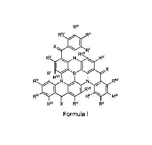
The organic light-emitting molecule of the invention comprises or consists of
a structure of
Formula I,
CA 3016778 2018-09-07
2
RIII
Riv RII
X
RI
Rvi
Rv Rv
X
RI
RIv
RNA
RIII RI
Riv X Rv RII
Formula I
In that Formula I:
X is at each occurrence independently from each other selected from the group
consisting of: 0,
S, NR 1 or C=C(CN)2.
R1 is at each occurrence independently from each other selected from the group
consisting of:
hydrogen, deuterium,
C1-05-alkyl,
which is optionally substituted with one or more substituents R2;
C6-C60-aryl,
which is optionally substituted with one or more substituents R2; and
C3-057-heteroaryl,
which is optionally substituted with one or more substituents R2.
RI, RI', RIII, Rv and Rvl is at each occurrence independently from each
other selected from the
group consisting of:
hydrogen, deuterium,
C1-040-alkyl,
which is optionally substituted with one or more substituents R2;
C1-C40-alkoxyl,
which is optionally substituted with one or more substituents R2;
C2-C40-alkenyl,
which is optionally substituted with one or more substituents R2;
C2-C40ralkynyl,
which is optionally substituted with one or more substituents R2;
CA 3016778 2018-09-07
3
C6-C60-aryl,
which is optionally substituted with one or more substituents R2;
C3-057-heteroaryl,
which is optionally substituted with one or more substituents R2;
CN, CF3, N(R2)2, OR2, and Si(R2)3.
R2 is at each occurrence independently from another selected from the group
consisting of:
hydrogen, deuterium, OPh, CF3, CN, F,
C1-05-alkyl,
wherein optionally one or more hydrogen atoms are independently from each
other
substituted by deuterium, CN, CF3, or F;
Cl-05-alkoxy,
wherein optionally one or more hydrogen atoms are independently from each
other
substituted by deuterium, CN, CF3, or F;
C1-05-thioalkoxy,
wherein optionally one or more hydrogen atoms are independently from each
other
substituted by deuterium, CN, CF3, or F;
02-05-alkenyl,
wherein optionally one or more hydrogen atoms are independently from each
other
substituted by deuterium, CN, CF3, or F;
C2-05-alkynyl,
wherein optionally one or more hydrogen atoms are independently from each
other
substituted by deuterium, CN, CF3, or F;
C6-C16-aryl,
which is optionally substituted with one or more C1-05-alkyl substituents;
C3-C17-heteroaryl,
which is optionally substituted with one or more C1-05-alkyl substituents;
N(C6-C15-ary1)2,
N(C3-017-heteroary1)2; and
N(C3-017-heteroary1)(C6-C15-aryl).
Optionally, at least one substituent selected from the group consisting of R1,
RI, RH, Fe, Riv IR"
and Ry1 forms a mono- or polycyclic, aliphatic, aromatic and/or benzo-fused
ring system with one
or more substituents selected from the group consisting of R1, RI, RII, RIv
Ry and RvI.
CA 3016778 2018-09-07
4
In a further embodiment of the invention, X is 0 at each occurrence.
In a further embodiment of the invention, wherein RI, R", RI", RI", Rv and RvI
is at each occurrence
independently from another selected from the group consisting of:
hydrogen, deuterium, halogen, Me, IPr, tBu, ON, CF3,
Ph, which is optionally substituted with one or more substituents
independently from each other
selected from the group consisting of Me, 'Pr, tBu, ON, CF3, and Ph,
pyridinyl, which is optionally substituted with one or more substituents
independently from each
other selected from the group consisting of Me, 'Pr, tBu, ON, CF3, and Ph,
pyrimidinyl, which is optionally substituted with one or more substituents
independently from each
other selected from the group consisting of Me, 'Pr, tBu, ON, CF3, and Ph,
carbazolyl, which is optionally substituted with one or more substituents
independently from each
other selected from the group consisting of Me, 'Pr, tBu, ON, CF3, and Ph,
triazinyl, which is optionally substituted with one or more substituents
independently from each
other selected from the group consisting of Me, 'Pr, tBu, ON, CF3, and Ph,
and N(Ph)2.
In a further embodiment of the invention, R", RIv and Rv is at each occurrence
independently from
another selected from the group consisting of:
hydrogen, deuterium, halogen, Me, 'Pr, tBu, ON, CF3,
Ph, which is optionally substituted with one or more substituents
independently from each other
selected from the group consisting of Me, 'Pr, tBu, CN, CF3, and Ph,
pyridinyl, which is optionally substituted with one or more substituents
independently from each
other selected from the group consisting of Me, 'Pr, tBu, ON, CF3, and Ph,
pyrimidinyl, which is optionally substituted with one or more substituents
independently from each
other selected from the group consisting of Me, 'Pr, tBu, ON, CF3, and Ph, and
triazinyl, which is optionally substituted with one or more substituents
independently from each
other selected from the group consisting of Me, 'Pr, tBu, CN, CF3, and Ph;
and RI, RI" and RvI is at each occurrence independently from another selected
from the group
consisting of hydrogen, deuterium, Me, 'Pr, tBu,
Ph, which is optionally substituted with one or more substituents
independently from each other
selected from the group consisting of Me, 'Pr, tBu, and Ph,
CA 3016778 2018-09-07
5
carbazolyl, which is optionally substituted with one or more substituents
independently from each
other selected from the group consisting of Me, 'Pr, tBu, CN, CF3, and Ph,
and N(Ph)2.
In a further embodiment of the invention, RH, RI" and Rv is at each occurrence
independently from
another selected from the group consisting of hydrogen, deuterium, Me, IPr,
'Bu, CN, CF3, and
Ph, which is optionally substituted with one or more substituents
independently from each other
selected from the group consisting of Me, 'Pr, ON, CF3, and Ph;
and RI, Rill and IV is at each occurrence independently from another selected
from the group
consisting of hydrogen, deuterium, Me, 'Pr, tBu,
Ph, which is optionally substituted with one or more substituents
independently from each other
selected from the group consisting of Me, 'Pr, tBu, and Ph,
carbazolyl, which is optionally substituted with one or more substituents
independently from each
other selected from the group consisting of Me, 'Bu, and Ph,
and N(Ph)2.
In a further embodiment of the invention, the organic molecules consist of a
structure of one of
Formulas ll to IX:
* 0
0 0
0
0
Formula II Formula III
CA 3016778 2018-09-07
6
INS
N
OS OS
N N
1.1 B 0 ISI B 0
N N N N
0 N J"CN . N N
0 0
1.1 lei
Formula IV Formula V
s
s 00
N
N
0 B S B S
N N
N N
S
S
Formula VI Formula VII
CA 3016778 2018-09-07
7
INS
S 110I S
= N
(101
N
Formula VIII Formula IX
In one embodiment, the molecule of the invention has a three-fold rotational
symmetry with the
central B atom of the molecule being the rotational axis.
As used throughout the present application, the terms "aryl" and "aromatic"
may be understood
in the broadest sense as any mono-, bi- or polycyclic aromatic moieties.
Accordingly, an aryl group
contains 6 to 60 aromatic ring atoms, and a heteroaryl group contains 5 to 60
aromatic ring atoms,
of which at least one is a heteroatom. Notwithstanding, throughout the
application the number of
aromatic ring atoms may be given as subscripted number in the definition of
certain substituents.
In particular, the heteroaromatic ring includes one to three heteroatoms.
Again, the terms
"heteroaryl" and "heteroaromatic" may be understood in the broadest sense as
any mono-, bi- or
polycyclic hetero-aromatic moieties that include at least one heteroatom. The
heteroatoms may
at each occurrence be the same or different and be individually selected from
the group consisting
of N, 0 and S. Accordingly, the term "arylene" refers to a divalent
substituent that bears two
binding sites to other molecular structures and thereby serving as a linker
structure. In case, a
group in the exemplary embodiments is defined differently from the definitions
given here, for
example, the number of aromatic ring atoms or number of heteroatoms differs
from the given
definition, the definition in the exemplary embodiments is to be applied.
According to the invention,
a condensed (annulated) aromatic or heteroaromatic polycycle is built of two
or more single
aromatic or heteroaromatic cycles, which formed the polycycle via a
condensation reaction.
CA 3016778 2018-09-07
8
In particular, as used throughout the present application, the term "aryl
group or heteroaryl group"
comprises groups which can be bound via any position of the aromatic or
heteroaromatic group,
derived from benzene, naphthaline, anthracene, phenanthrene, pyrene,
dihydropyrene, chrysene,
perylene, fluoranthene, benzanthracene, benzphenanthrene, tetracene,
pentacene, benzpyrene,
furan, benzofuran, isobenzofuran, dibenzofuran, thiophene, benzothiophene,
isobenzothiophene,
dibenzothiophene; pyrrole, indole, isoindole, carbazole, pyridine, quinoline,
isoquinoline, acridine,
phenanthridine, benzo-5,6-quinoline, benzo-6,7-quinoline, benzo-7,8-quinoline,
phenothiazine,
phenoxazine, pyrazole, indazole, imidazole,
benzimidazole, naphthoimidazole,
phenanthroimidazole, pyridoimidazole, pyrazinoimidazole, quinoxalinoimidazole,
oxazole,
benzoxazole, napthooxazole, anthroxazol, phenanthroxazol, isoxazole, 1,2-
thiazole, 1,3-thiazole,
benzothiazole, pyridazine, benzopyridazine, pyrimidine, benzopyrimidine, 1,3,5-
triazine,
quinoxaline, pyrazine, phenazine, naphthyridine, carboline, benzocarboline,
phenanthroline,
1,2,3-triazole, 1,2,4-triazole, benzotriazole, 1,2,3-oxadiazole, 1,2,4-
oxadiazole, 1,2,5-oxadiazole,
1,2,3,4-tetrazine, purine, pteridine, indolizine and benzothiadiazole or
combinations of the
abovementioned groups.
As used throughout the present application, the term "cyclic group" may be
understood in the
broadest sense as any mono-, bi- or polycyclic moieties.
As used throughout the present application, the term "biphenyl" as a
substituent may be
understood in the broadest sense as ortho-biphenyl, meta-biphenyl, or para-
biphenyl, wherein
ortho, meta and para is defined in regard to the binding site to another
chemical moiety.
As used throughout the present application, the term "alkyl group" may be
understood in the
broadest sense as any linear, branched, or cyclic alkyl substituent. In
particular, the term alkyl
comprises the substituents methyl (Me), ethyl (Et), n-propyl ("Pr), i-propyl
('Pr), cyclopropyl, n-
butyl ("Bu), i-butyl (Bu), s-butyl (sBu), t-butyl ('Bu), cyclobutyl, 2-
methylbutyl, n-pentyl, s-pentyl, t-
pentyl, 2-pentyl, neo-pentyl, cyclopentyl, n-hexyl, s-hexyl, t-hexyl, 2-hexyl,
3-hexyl, neo-hexyl,
cyclohexyl, 1-methylcyclopentyl, 2-methylpentyl, n-heptyl, 2-heptyl, 3-heptyl,
4-heptyl,
cycloheptyl, 1-methylcyclohexyl, n-octyl, 2-ethylhexyl, cyclooctyl, 1-
bicyclo[2,2,2]octyl, 2-
bicyclo[2,2,2]-octyl, 2-(2,6-dimethyl)octyl, 3-(3,7-dimethyl)octyl, adamantyl,
2,2,2-trifluorethyl,
1,1-dimethyl-n-hex-1-yl, 1 ,1-dimethyl-n-hept-1-yl, 1 ,1-dimethyl-n-oct-1-yl,
1,1-dimethyl-n-dec-1-
yl, 1,1-dimethyl-n-dodec-1-yl, 1,1-dimethyl-n-tetradec-1-yl, 1,1-dimethyl-n-
hexadec-1-yl, 1 ,1-
d imethyl-n-octadec-1 -yl, 1 ,1-diethyl-n-hex-1-yl, 1 ,1-diethyl-n-hept-1-yl,
1 ,1-diethyl-n-oct-1-yl, 1,1-
CA 3016778 2018-09-07
9
diethyl-n-dec-1-yl, 1,1-diethyl-n-dodec-1-yl, 1,1-diethyl-n-tetradec-1-yl, 1,1-
diethyln-n-hexadec-1-
yl, 1,1-diethyl-n-octadec-1-yl, 1-(n-propyI)-cyclohex-1-yl, 1-(n-butyl)-
cyclohex-1-yl, 1-(n-hexyl)-
cyclohex-1-yl, 1-(n-octy1)-cyclohex-1-y1 and 1-(n-decy1)-cyclohex-1-yl.
As used throughout the present application, the term "alkenyl" comprises
linear, branched, and
cyclic alkenyl substituents. The term alkenyl group exemplarily comprises the
substituents
ethenyl, propenyl, butenyl, pentenyl, cyclopentenyl, hexenyl, cyclohexenyl,
heptenyl,
cycloheptenyl, octenyl, cyclooctenyl or cyclooctadienyl.
As used throughout the present application, the term "alkynyl" comprises
linear, branched, and
cyclic alkynyl substituents. The term alkynyl group exemplarily comprises
ethynyl, propynyl,
butynyl, pentynyl, hexynyl, heptynyl or octynyl.
As used throughout the present application, the term "alkoxy" comprises
linear, branched, and
cyclic alkoxy substituents. The term alkoxy group exemplarily comprises
methoxy, ethoxy, n-
propoxy, i-propoxy, n-butoxy, s-butoxy, t-butoxy and 2-methylbutoxy.
As used throughout the present application, the term "thioalkoxy" comprises
linear, branched, and
cyclic thioalkoxy substituents, in which the 0 of the exemplarily alkoxy
groups is replaced by S.
As used throughout the present application, the terms "halogen" and "halo" may
be understood
in the broadest sense as being preferably fluorine, chlorine, bromine or
iodine.
Whenever hydrogen (H) is mentioned herein, it could also be replaced by
deuterium at each
occurrence.
It is understood that when a molecular fragment is described as being a
substituent or otherwise
attached to another moiety, its name may be written as if it were a fragment
(e.g. naphtyl,
dibenzofuryl) or as if it were the whole molecule (e.g. naphthalene,
dibenzofuran). As used herein,
these different ways of designating a substituent or attached fragment are
considered to be
equivalent.
In one embodiment, the organic molecules according to the invention have an
excited state
lifetime of not more than 150 ps, of not more than 100 ps, in particular of
not more than 50 ps,
CA 3016778 2018-09-07
10
more preferably of not more than 10 ps or not more than 7 ps in a film of
poly(methyl methacrylate)
(PMMA) with 10 % by weight of organic molecule at room temperature.
In a further embodiment of the invention, the organic molecules according to
the invention have
an emission peak in the visible or nearest ultraviolet range, i.e., in the
range of a wavelength of
from 380 to 800 nm, with a full width at half maximum of less than 0.40 eV,
preferably less than
0.35 eV, more preferably less than 0.33 eV, even more preferably less than
0.30 eV or even less
than 0.28 eV in a film of poly(methyl methacrylate) (PMMA) with 10 % by weight
of organic
molecule at room temperature.
Orbital and excited state energies can be determined either by means of
experimental methods
or by calculations employing quantum-chemical methods, in particular density
functional theory
calculations. The energy of the highest occupied molecular orbital EFI m is
determined by
methods known to the person skilled in the art from cyclic voltammetry
measurements with an
accuracy of 0.1 eV. The energy of the lowest unoccupied molecular orbital Ewm
is calculated as
EHomo Egap,
wherein EgaP is determined as follows: For host compounds, the onset of the
emission spectrum of a film with 10 A) by weight of host in poly(methyl
methacrylate) (PMMA) is
used as EgaP, unless stated otherwise. For emitter molecules, Egag is
determined as the energy at
which the excitation and emission spectra of a film with 10 % by weight of
emitter in PMMA cross.
The energy of the first excited triplet state Ti is determined from the onset
of the emission
spectrum at low temperature, typically at 77 K. For host compounds, where the
first excited singlet
state and the lowest triplet state are energetically separated by > 0.4 eV,
the phosphorescence is
usually visible in a steady-state spectrum in 2-Me-THF. The triplet energy can
thus be determined
as the onset of the phosphorescence spectrum. For TADF emitter molecules, the
energy of the
first excited triplet state Ti is determined from the onset of the delayed
emission spectrum at 77
K, if not otherwise stated, measured in a film of PMMA with 10% by weight of
emitter. Both for
host and emitter compounds, the energy of the first excited singlet state Si
is determined from
the onset of the emission spectrum, if not otherwise stated, measured in a
film of PMMA with
% by weight of host or emitter compound.
The onset of an emission spectrum is determined by computing the intersection
of the tangent to
the emission spectrum with the x-axis. The tangent to the emission spectrum is
set at the high-
CA 3016778 2018-09-07
11
energy side of the emission band and at the point at half maximum of the
maximum intensity of
the emission spectrum.
A further aspect of the invention relates to a process for preparing the
organic molecule of the
invention (with an optional subsequent reaction), wherein tert-butyllithium
(tBuLi) and boron
tribromide (BBr3) is used as a reactant:
0 Rvi
0 Cu
Br Br K2CO3 Fiv N I" Rv
+ NH2 ___________ v.
Rv iel Xylene Rvl
180 C
Rvi Br Br
El E2 ZI
.
,
4,
0 Rvi 0
Rvi
Pd(0A02
Ftv N Rv CI PtBu3 Rv N
Ry1 40
Rv
H2N 0 NH2 NaOtBu lei SI
0 + ______________________________________________________ = CI
Br Br RNA Xylene, Rvi HN 0 NH
reflux
Rv
Rvi
Z1 E3 Rv
Z2
=
0 Rvi H Rvi
RV N RV Rv N Rv
Rvi 01 CI Si KOH __________ ),.. RVI 401 CI
HN 0 NH i-PrOH, Xylene HN NH
70 C
0
Rvi el
RV RV
Z2 Z3
1 CA 3016778 2018-09-07
12
Rill
RIv RII
RVI X
H RI
Rv N RV Me0 X Cu/Cul Rvi
OMe
K2CO3 R''N
Rv
I RIv >
RvI CI $1 + Rvi 0 40
Ph20,190 C
OMe
RI RI
HN 0 NH = CI
II RI
X
Rvi RII RH N N Fe/
0 Rvi ,
RV Rill OMe RI
Rill
Z3 E4 Riv x Rv RH
Z4
RI" RIII
RIV RH RN R"
X X
R1 RI
OMe
RvI LiOH OH Rvi
Rv N Rv ___________________ )1.- Rõ v N Rv
THF/Me0H/H20
RNA 40 ill OH
RNA 0 40 OMe reflux CI
RI CI X RI
X
RII N N Riv R" N N
RN
IS) Rvi lel Rvi
RI" OMe RI RI" RI" RI
RI"
Rv Riv x OH
RV
RN x R" RII
Z4 Z5
RIII RIII
RN/ R" RN R"
X RI XIIX
RI
OH R" Rvi
R''N Rv POCI3 RV N RV
__________________________________________________ ii.
R" 110 (10 OH X
MeCN CI
RI CI X H20 R" R1 Rvi
N N
Riv
RIII el
R" N N Riv reflux - rt Rvi
RVI
RI"
R" RI RI"
RN X III
OH RV RIv X Rv R"
RI R
Z5 Z6
1 CA 3016778 2018-09-07
13
Rill
RN R" RR/ RH
X X
RI RI
Rvi NA
Rv N RV 1. tBuLi, -30 C to 0 C Rv NR RV
2. BBr3, -30 C to RT to 120 C
X 3. N,N-DIPEA 0 C to 120 C X
RI CI _________________________ x RI B
RvIN RNA
R" N Riv tert-butylbenzene RII N N RR/
Rvi RNA
Rill RI Rol RI" RI RIII
Fe/ X Rv R11 RI" X IV R"
Z6 P1
A further aspect of the invention relates to the use of an organic molecule of
the invention as a
luminescent emitter or as an absorber, and/or as a host material and/or as an
electron transport
material, and/or as a hole injection material, and/or as a hole blocking
material in an optoelectronic
device.
A preferred embodiment relates to the use of an organic molecule according to
the invention as
a luminescent emitter in an optoelectronic device.
The optoelectronic device may be understood in the broadest sense as any
device based on
organic materials that is suitable for emitting light in the visible or
nearest ultraviolet (UV) range,
i.e., in the range of a wavelength of from 380 to 800 nm. More preferably,
optoelectronic device
may be able to emit light in the visible range, i.e., of from 380 nm to 800
nm.
In the context of such use, the optoelectronic device is more particularly
selected from the group
consisting of:
= organic light-emitting diodes (OLEDs),
= light-emitting electrochemical cells,
= OLED sensors, especially in gas and vapor sensors that are not
hermetically shielded to
the surroundings,
= organic diodes,
= organic solar cells,
= organic transistors,
= organic field-effect transistors,
= organic lasers and
CA 3016778 2018-09-07
14
= down-conversion elements.
In a preferred embodiment in the context of such use, the optoelectronic
device is a device
selected from the group consisting of an organic light emitting diode (OLED),
a light emitting
electrochemical cell (LEC), and a light-emitting transistor.
In the case of the use, the fraction of the organic molecule according to the
invention in the
emission layer in an optoelectronic device, more particularly in an OLED, is 1
% to 99 % by weight,
more particularly 3 % to 80 % by weight. In an alternative embodiment, the
proportion of the
organic molecule in the emission layer is 100 % by weight.
A further aspect of the invention relates to a composition comprising or
consisting of:
(a) at least one organic molecule according to the invention, in particular
in the form of an
emitter and/or a host, and
(b) one or more emitter and/or host materials, which differ from the
organic molecule
according to the invention and
(c) optionally, one or more dyes and/or one or more solvents.
In one embodiment, the light-emitting layer of an optoelectronic device, in
particular of an OLED,
comprises not only the organic molecules according to the invention, but also
a host material
whose triplet (Ti) and singlet (Si) energy levels are energetically higher
than the triplet (Ti) and
singlet (Si) energy levels of the organic molecule.
In one embodiment, the light-emitting layer comprises (or essentially consists
of) a composition
comprising or consisting of:
(a) at least one organic molecule according to the invention, in particular
in the form of an
emitter and/or a host, and
(b) one or more emitter and/or host materials, which differ from the
organic molecule
according to the invention and
(c) optionally, one or more dyes and/or one or more solvents.
In a particular embodiment, the light-emitting layer EML comprises (or
essentially consists of) a
composition comprising or consisting of:
CA 3016778 2018-09-07
15
(i) 1-50 % by weight, preferably 5-40 % by weight, in particular 10-30 % by
weight, of one or
more organic molecules according to the invention;
(ii) 5-99 % by weight, preferably 30-94.9 % by weight, in particular 40-89%
by weight, of at
least one host compound H; and
(iii) optionally 0-94 % by weight, preferably 0.1-65 % by weight, in
particular 1-50 % by weight,
of at least one further host compound D with a structure differing from the
structure of the
molecules according to the invention; and
(iv) optionally 0-94 % by weight, preferably 0-65 % by weight, in
particular 0-50 % by weight,
of a solvent; and
(v) optionally 0-30 % by weight, in particular 0-20 % by weight, preferably
0-5 % by weight, of
at least one further emitter molecule F with a structure differing from the
structure of the
molecules according to the invention.
Preferably, energy can be transferred from the host compound H to the one or
more organic
molecules according to the invention, in particular transferred from the first
excited triplet state
TI (H) of the host compound H to the first excited triplet state TI (E) of the
one or more organic
molecules according to the invention E and/or from the first excited singlet
state Si (H) of the host
compound H to the first excited singlet state S1(E) of the one or more organic
molecules according
to the invention E.
In a further embodiment, the light-emitting layer EML comprises (or
essentially consists of) a
composition comprising or consisting of:
(i) 1-50 % by weight, preferably 5-40 % by weight, in particular 10-30 % by
weight, of one
organic molecule according to the invention;
(ii) 5-99 % by weight, preferably 30-94.9 `)/0 by weight, in particular 40-
89% by weight, of one
host compound H; and
(iii) optionally 0-94% by weight, preferably 0.1-65% by weight, in
particular 1-50% by weight,
of at least one further host compound D with a structure differing from the
structure of the
molecules according to the invention; and
(iv) optionally 0-94 % by weight, preferably 0-65 % by weight, in
particular 0-50 % by weight,
of a solvent; and
(v) optionally 0-30 % by weight, in particular 0-20 % by weight, preferably
0-5 % by weight, of
at least one further emitter molecule F with a structure differing from the
structure of the
molecules according to the invention.
CA 3016778 2018-09-07
16
In one embodiment, the host compound H has a highest occupied molecular
orbital HOMO(H)
having an energy EN m (H) in the range of from -5 to -6.5 eV and the at least
one further host
compound D has a highest occupied molecular orbital HOMO(D) having an energy
Ell m (D),
wherein EHOMO(H) > EHOMO(D).
In a further embodiment, the host compound H has a lowest unoccupied molecular
orbital
LUMO(H) having an energy El-um (H) and the at least one further host compound
D has a lowest
unoccupied molecular orbital LUMO(D) having an energy ELum (D), wherein
ELumo(H) > ELumo(D).
In one embodiment, the host compound H has a highest occupied molecular
orbital HOMO(H)
having an energy E1-1 "^ (H) and a lowest unoccupied molecular orbital LUMO(H)
having an energy
El-um (H), and
the at least one further host compound D has a highest occupied molecular
orbital
HOMO(D) having an energy EH m (D) and a lowest unoccupied molecular orbital
LUMO(D)
having an energy ELum(D),
the organic molecule according to the invention E has a highest occupied
molecular orbital
HOMO(E) having an energy EI-1 m (E) and a lowest unoccupied molecular orbital
LUMO(E) having
an energy ELum (E),
wherein
EHomo(d) > EHom (D) and the difference between the energy level of the highest
occupied
molecular orbital HOMO(E) of the organic molecule according to the invention E
(E1-1 m (E)) and
the energy level of the highest occupied molecular orbital HOMO(H) of the host
compound H
(EHm (H)) is between -0.5 eV and 0.5 eV, more preferably between -0.3 eV and
0.3 eV, even
more preferably between -0.2 eV and 0.2 eV or even between -0.1 eV and 0.1 eV;
and
ELumo(H) > ELumoi
kD) and the difference between the energy level of the lowest unoccupied
molecular orbital LUMO(E) of the organic molecule according to the invention E
(ELum (E)) and
the lowest unoccupied molecular orbital LUMO(D) of the at least one further
host compound D
(Eww(D)) is between -0.5 eV and 0.5 eV, more preferably between -0.3 eV and
0.3 eV, even
more preferably between -0.2 eV and 0.2 eV or even between -0.1 eV and 0.1 eV.
In one embodiment of the invention, the host compound D and/or the host
compound H is a
thermally-activated delayed fluorescence (TADF)-material. TADF materials
exhibit a LEST value,
which corresponds to the energy difference between the first excited singlet
state (Si) and the
CA 3016778 2018-09-07
17
first excited triplet state (T1), of less than 2500 cm-1. Preferably the TADF
material exhibits a
LEST value of less than 3000 cm-1, more preferably less than 1500 cm-1, even
more preferably
less than 1000 cm-1 or even less than 500 cm-1.
In one embodiment, the host compound D is a TADF material and the host
compound H exhibits
a AEsT value of more than 2500 cm-1. In a particular embodiment, the host
compound D is a TADF
material and the host compound H is selected from group consisting of CBP,
mCP, mCBP, 9-[3-
(dibenzofuran-2-yl)pheny1]-9H-carbazole, 9[3-(dibenzofuran-2-yl)pheny1]-9H-
carbazole, 943-
(dibenzothiophen-2-yflpheny1]-9H-carbazole, 943,5-bis(2-dibenzofuranyflpheny1]-
9H-carbazole
and 9[3,5-bis(2-dibenzothiophenyl)pheny1]-9H-carbazole.
In one embodiment, the host compound H is a TADF material and the host
compound D exhibits
a LEST value of more than 2500 cm-1. In a particular embodiment, the host
compound H is a TADF
material and the host compound D is selected from group consisting of T2T
(2,4,6-tris(bipheny1-
3-y1)-1,3,5-triazine), T3T (2,4,6-tris(tripheny1-3-y1)-1,3,5-triazine) and/or
TST (2,4,6-tris(9,9'-
spirobifluorene-2-y1)-1,3,5-triazine).
In a further aspect, the invention relates to an optoelectronic device
comprising an organic
molecule or a composition of the type described here, more particularly in the
form of a device
selected from the group consisting of organic light-emitting diode (OLED),
light-emitting
electrochemical cell, OLED sensor, more particularly gas and vapour sensors
not hermetically
externally shielded, organic diode, organic solar cell, organic transistor,
organic field-effect
transistor, organic laser and down-conversion element.
In a preferred embodiment, the optoelectronic device is a device selected from
the group
consisting of an organic light emitting diode (OLED), a light emitting
electrochemical cell (LEC),
and a light-emitting transistor.
In one embodiment of the optoelectronic device of the invention, the organic
molecule according
to the invention E is used as an emission material in a light-emitting layer
EML.
In one embodiment of the optoelectronic device of the invention, the light-
emitting layer EML
consists of the composition according to the invention described here.
CA 3016778 2018-09-07
18
When the optoelectronic device is an OLED, it may, for example, have the
following layer
structure:
1. substrate
2. anode layer A
3. hole injection layer, HIL
4. hole transport layer, HTL
5. electron blocking layer, EBL
6. emitting layer, EML
7. hole blocking layer, HBL
8. electron transport layer, ETL
9. electron injection layer, EIL
10. cathode layer,
wherein the OLED comprises each layer selected from the group of HIL, HTL,
EBL, HBL, ETL,
and EIL only optionally, different layers may be merged and the OLED may
comprise more than
one layer of each layer type defined above.
Furthermore, the optoelectronic device may, in one embodiment, comprise one or
more protective
layers protecting the device from damaging exposure to harmful species in the
environment
including, for example, moisture, vapor and/or gases.
In one embodiment of the invention, the optoelectronic device is an OLED, with
the following
inverted layer structure:
1. substrate
2. cathode layer
3. electron injection layer, EIL
4. electron transport layer, ETL
5. hole blocking layer, HBL
6. emitting layer, B
7. electron blocking layer, EBL
8. hole transport layer, HTL
9. hole injection layer, HIL
10. anode layer A
CA 3016778 2018-09-07
19
wherein the OLED comprises each layer selected from the group of HIL, HTL,
EBL, HBL, ETL,
and EIL only optionally, different layers may be merged and the OLED may
comprise more than
one layer of each layer types defined above.
In one embodiment of the invention, the optoelectronic device is an OLED,
which may have a
stacked architecture. In this architecture, contrary to the typical
arrangement in which the OLEDs
are placed side by side, the individual units are stacked on top of each
other. Blended light may
be generated with OLEDs exhibiting a stacked architecture, in particular white
light may be
generated by stacking blue, green and red OLEDs. Furthermore, the OLED
exhibiting a stacked
architecture may comprise a charge generation layer (CGL), which is typically
located between
two OLED subunits and typically consists of a n-doped and p-doped layer with
the n-doped layer
of one CGL being typically located closer to the anode layer.
In one embodiment of the invention, the optoelectronic device is an OLED,
which comprises two
or more emission layers between anode and cathode. In particular, this so-
called tandem OLED
comprises three emission layers, wherein one emission layer emits red light,
one emission layer
emits green light and one emission layer emits blue light, and optionally may
comprise further
layers such as charge generation layers, blocking or transporting layers
between the individual
emission layers. In a further embodiment, the emission layers are adjacently
stacked. In a further
embodiment, the tandem OLED comprises a charge generation layer between each
two emission
layers. In addition, adjacent emission layers or emission layers separated by
a charge generation
layer may be merged.
The substrate may be formed by any material or composition of materials. Most
frequently, glass
slides are used as substrates. Alternatively, thin metal layers (e.g., copper,
gold, silver or
aluminum films) or plastic films or slides may be used. This may allow for a
higher degree of
flexibility. The anode layer A is mostly composed of materials allowing to
obtain an (essentially)
transparent film. As at least one of both electrodes should be (essentially)
transparent in order to
allow light emission from the OLED, either the anode layer A or the cathode
layer C is transparent.
Preferably, the anode layer A comprises a large content or even consists of
transparent
conductive oxides (TC0s). Such anode layer A may, for example, comprise indium
tin oxide,
aluminum zinc oxide, fluorine doped tin oxide, indium zinc oxide, Pb0, SnO,
zirconium oxide,
molybdenum oxide, vanadium oxide, tungsten oxide, graphite, doped Si, doped
Ge, doped GaAs,
doped polyaniline, doped polypyrrol and/or doped polythiophene.
CA 3016778 2018-09-07
20
The anode layer A (essentially) may consist of indium tin oxide (ITO) (e.g.,
(In03)0.9(Sn02)01). The
roughness of the anode layer A caused by the transparent conductive oxides
(TC0s) may be
compensated by using a hole injection layer (HIL). Further, the HIL may
facilitate the injection of
quasi charge carriers (i.e., holes) in that the transport of the quasi charge
carriers from the TCO
to the hole transport layer (HTL) is facilitated. The hole injection layer
(H1L) may comprise poly-
3,4-ethylendioxy thiophene (PEDOT), polystyrene sulfonate (PSS), Mo02, V205,
CuPC or Cul, in
particular a mixture of PEDOT and PSS. The hole injection layer (HIL) may also
prevent the
diffusion of metals from the anode layer A into the hole transport layer
(HTL). The HIL may
exemplarily comprise PEDOT:PSS (poly-3,4-ethylendioxy thiophene: polystyrene
sulfonate),
PE DOT (poly-3,4-ethylendioxy thiophene),
mMTDATA (4,4',4"-tris[phenyl(m-
tolyl)amino]triphenylamine), Spiro-
TAD (2,2',7,7'-tetrakis(n,n-diphenylamino)-9,9'-
spirobifluorene), DNTPD (N1 ,N1-(bipheny1-4,4'-diy1)bis(N1-phenyl-N4,N4-di-m-
tolylbenzene-1 ,4-
diamine), NPB (N,N'-nis-(1-naphthalenyI)-N,N'-bis-phenyl-(1,1'-bipheny1)-4,4'-
diamine), NPNPB
(N,N1-diphenyl-NN-di-[4-(N,N-diphenyl-amino)phenyl]benzidine), Me0-
TPD (N,N,N',N'-
tetrakis(4-methoxyphenyl)benzidine), HAT-
CN (1 ,4,5,8,9,1 1 -hexaazatriphenylen-
hexacarbonitrile) and/or Spiro-NPD (N,N'-diphenyl-N,N'-bis-(1-naphthyl)-9,9'-
spirobifluorene-2,7-
diarnine).
Adjacent to the anode layer A or hole injection layer (HIL), a hole transport
layer (HTL) is typically
located. Herein, any hole transport compound may be used. For example,
electron-rich
heteroaromatic compounds such as triarylamines and/or carbazoles may be used
as hole
transport compound. The HTL may decrease the energy barrier between the anode
layer A and
the light-emitting layer EML. The hole transport layer (HTL) may also be an
electron blocking layer
(EBL). Preferably, hole transport compounds bear comparably high energy levels
of their triplet
states T1. For example, the hole transport layer (HTL) may comprise a star-
shaped heterocycle
such as tris(4-carbazoy1-9-ylphenyl)amine (TCTA), poly-TPD (poly(4-butylphenyl-
diphenyl-
amine)), [alpha]-NPD (poly(4-butylphenyl-diphenyl-amine)), TAPC (4,4'-
cyclohexyliden-bis[N,N-
bis(4-methylphenyl)benzenamine]), 2-TNATA
(4,4',4"-tris[2-
naphthyl(phenyl)amino]triphenylamine), Spiro-TAD, DNTPD, NPB, NPNPB, Me0-TPD,
HAT-CN
and/or TrisPcz (9,9'-dipheny1-6-(9-pheny1-9H-carbazol-3-y1)-9H,9'H-3,3'-
bicarbazole). In addition,
the HTL may comprise a p-doped layer, which may be composed of an inorganic or
organic
dopant in an organic hole-transporting matrix. Transition metal oxides such as
vanadium oxide,
molybdenum oxide or tungsten oxide may exemplarily be used as inorganic
dopant.
CA 3016778 2018-09-07
21
Tetrafluorotetracyanoquinodimethane (F4-TCNQ), copper-pentafluorobenzoate
(Cu(l)pFBz) or
transition metal complexes may exemplarily be used as organic dopant.
The EBL may exemplarily comprise mCP (1,3-bis(carbazol-9-yl)benzene), TCTA, 2-
TNATA,
mCBP (3,3-di(9H-carbazol-9-yl)biphenyl), tris-Pcz, CzSi
(9-(4-tert-Butylpheny1)-3,6-
bis(triphenylsily1)-9H-carbazole), and/or DCB (N,N'-dicarbazolyI-1,4-
dimethylbenzene).
Adjacent to the hole transport layer (HTL), the light-emitting layer EML is
typically located. The
light-emitting layer EML comprises at least one light emitting molecule.
Particularly, the EML
comprises at least one light emitting molecule according to the invention E.
In one embodiment,
the light-emitting layer comprises only the organic molecules according to the
invention. Typically,
the EML additionally comprises one or more host materials H. Exemplarily, the
host material H is
selected from CBP (4,4'-Bis-(N-carbazolyI)-biphenyl), mCP, mCBP Sif87
(dibenzo[b,d]thiophen-
2-yltriphenylsilane), CzSi, Sif88 (dibenzo[b,d]thiophen-2-yl)diphenylsilane),
DPEPO (bis[2-
(diphenylphosphino)phenyl] ether oxide), 943-(dibenzofuran-2-yl)pheny1]-9H-
carbazole, 943-
(dibenzofuran-2-yl)phenyI]-9H-carbazole, 9[3-(dibenzothiophen-2-yl)pheny1]-9H-
carbazole, 9-
[3,5-bis(2-dibenzofu ranyl)phenyI]-9 H-carbazole, 943,5-
bis(2-dibenzothiophenyl)pheny1]-9H-
carbazole, T2T (2,4,6-tris(bipheny1-3-y1)-1,3,5-triazine), T3T (2,4,6-
tris(tripheny1-3-y1)-1,3,5-
triazine) and/or TST (2,4,64ris(9,91-spirobifluorene-2-y1)-1,3,5-triazine).
The host material H
typically should be selected to exhibit first triplet (T1) and first singlet
(Si) energy levels, which
are energetically higher than the first triplet (Ti) and first singlet (Si)
energy levels of the organic
molecule.
In one embodiment of the invention, the EML comprises a so-called mixed-host
system with at
least one hole-dominant host and one electron-dominant host. In a particular
embodiment, the
EML comprises exactly one light emitting organic molecule according to the
invention and a
mixed-host system comprising T2T as electron-dominant host and a host selected
from CBP,
mCP, mCBP, 9[3-(dibenzofuran-2-yl)pheny11-9H-carbazole, 943-(dibenzofuran-2-
yl)pheny1]-9H-
carbazole, 9[3-(dibenzothiophen-2-yl)pheny1]-9H-carbazole, 9-
[3,5-bis(2-
dibenzofuranyl)phenyI]-9H-carbazole and 943,5-bis(2-dibenzothiophenyl)pheny1]-
9H-carbazole
as hole-dominant host. In a further embodiment the EML comprises 50-80 % by
weight, preferably
60-75 % by weight of a host selected from CBP, mCP, mCBP, 943-(dibenzofuran-2-
yl)phenylj-
9H-carbazole, 9[3-(dibenzofuran-2-yl)pheny1]-9H-carbazole, 913-
(dibenzothiophen-2-yl)phenylF
9 H-carbazole, 9[3,5-bis(2-dibenzofuranyl)pheny1]-9H-carbazole and
9-[3,5-bis(2-
CA 3016778 2018-09-07
22
dibenzothiophenyl)phenyI]-9H-carbazole; 10-45 % by weight, preferably 15-30 %
by weight of
T2T and 5-40 % by weight, preferably 10-30 % by weight of light emitting
molecule according to
the invention.
Adjacent to the light-emitting layer EML, an electron transport layer (ETL)
may be located. Herein,
any electron transporter may be used. Exemplarily, electron-poor compounds
such as, e.g.,
benzimidazoles, pyridines, triazoles, oxadiazoles (e.g., 1,3,4-oxadiazole),
phosphinoxides and
sulfone, may be used. An electron transporter may also be a star-shaped
heterocycle such as
1,3,5-tri(1-pheny1-1H-benzo[d]imidazol-2-yl)phenyl (TPBi). The ETL may
comprise NBphen (2,9-
bis(naphthalen-2-y1)-4,7-dipheny1-1,10-phenanth roline), Alq3
(Aluminum-tris(8-
hydroxyquinoline)), TSPO1 (dipheny1-4-triphenylsilylphenyl-phosphinoxide),
BPyTP2 (2,7-di(2,2'-
bipyridin-5-yl)triphenyle), Sif87
(dibenzo[b,d]thiophen-2-yltriphenylsilane), Sif88
(dibenzo[b,d]thiophen-2-yl)diphenylsilane),
BmPyPhB (1,3-bis[3,5-di(pyridin-3-
yl)phenyl]benzene) and/or BTB (4,4'-bis42-(4,6-dipheny1-1,3,5-triaziny1)]-1,1'-
biphenyl).
Optionally, the ETL may be doped with materials such as Liq. The electron
transport layer (ETL)
may also block holes or a holeblocking layer (HBL) is introduced.
The HBL may, for example, comprise BCP (2,9-dimethy1-4,7-dipheny1-1,10-
phenanthroline =
Bathocuproine), BAlq (bis(8-hydroxy-2-methylquinoline)-(4-
phenylphenoxy)aluminum), NBphen
(2,9-bis(naphthalen-2-yI)-4,7-dipheny1-1,10-phenanthroline), Alq3
(Aluminum-tris(8-
hydroxyquinoline)), TSPO1 (dipheny1-4-triphenylsilylphenyl-phosphinoxide), T2T
(2,4,6-
tris(bipheny1-3-y1)-1,3,5-triazine), T3T (2,4,6-tris(tripheny1-3-y1)-1,3,5-
triazine), TST (2,4,6-
tris(9,9'-spirobifluorene-2-yI)-1,3,5-triazine), and/or TCBTTCP (1,3,5-tris(N-
carbazolyl)benzol/
1,3,5-tris(carbazol)-9-y1) benzene).
Adjacent to the electron transport layer (ETL), a cathode layer C may be
located. The cathode
layer C may, for example, comprise or may consist of a metal (e.g., Al, Au,
Ag, Pt, Cu, Zn, Ni, Fe,
Pb, LiF, Ca, Ba, Mg, In, W, or Pd) or a metal alloy. For practical reasons,
the cathode layer may
also consist of (essentially) intransparent metals such as Mg, Ca or Al.
Alternatively or
additionally, the cathode layer C may also comprise graphite and or carbon
nanotubes (CNTs).
Alternatively, the cathode layer C may also consist of nanoscalic silver
wires.
An OLED may further, optionally, comprise a protection layer between the
electron transport layer
(ETL) and the cathode layer C (which may be designated as electron injection
layer (EIL)). This
CA 3016778 2018-09-07
23
layer may comprise lithium fluoride, cesium fluoride, silver, Liq (8-
hydroxyquinolinolatolithium),
Li2O, BaF2, MgO and/or NaF.
Optionally, the electron transport layer (ETL) and/or a hole blocking layer
(HBL) may also
comprise one or more host compounds H.
In order to modify the emission spectrum and/or the absorption spectrum of the
light-emitting layer
EML further, the light-emitting layer EML may further comprise one or more
further emitter
molecules F. Such an emitter molecule F may be any emitter molecule known in
the art. Preferably
such an emitter molecule F is a molecule with a structure differing from the
structure of the
molecules according to the invention E. The emitter molecule F may optionally
be a TADF emitter.
Alternatively, the emitter molecule F may optionally be a fluorescent and/or
phosphorescent
emitter molecule which is able to shift the emission spectrum and/or the
absorption spectrum of
the light-emitting layer EML. For example, the triplet and/or singlet excitons
may be transferred
from the organic emitter molecule according to the invention to the emitter
molecule F before
relaxing to the ground state SO by emitting light typically red-shifted in
comparison to the light
emitted by an organic molecule. Optionally, the emitter molecule F may also
provoke two-photon
effects (i.e., the absorption of two photons of half the energy of the
absorption maximum).
Optionally, an optoelectronic device (e.g., an OLED) may, for example, be an
essentially white
optoelectronic device. Exemplarily such white optoelectronic device may
comprise at least one
(deep) blue emitter molecule and one or more emitter molecules emitting green
and/or red light.
Then, there may also optionally be energy transmittance between two or more
molecules as
described above.
As used herein, if not defined more specifically in the particular context,
the designation of the
colors of emitted and/or absorbed light is as follows:
violet: wavelength range of >380-420 nm;
deep blue: wavelength range of >420-480 nm;
sky blue: wavelength range of >480-500 nm;
green: wavelength range of >500-560 nm;
yellow: wavelength range of >560-580 nm;
orange: wavelength range of >580-620 nm;
CA 3016778 2018-09-07
24
red: wavelength range of >620-800 nm.
With respect to emitter molecules, such colors refer to the emission maximum.
Therefore,
exemplarily, a deep blue emitter has an emission maximum in the range of from
>420 to 480 nm,
a sky blue emitter has an emission maximum in the range of from >480 to 500
nm, a green emitter
has an emission maximum in a range of from >500 to 560 nm, a red emitter has
an emission
maximum in a range of from >620 to 800 nm.
A deep blue emitter may preferably have an emission maximum of below 480 nm,
more preferably
below 470 nm, even more preferably below 465 nm or even below 460 nm. It will
typically be
above 420 nm, preferably above 430 nm, more preferably above 440 nm or even
above 450 nm.
Accordingly, a further aspect of the present invention relates to an OLED,
which exhibits an
external quantum efficiency at 1000 cd/m2 of more than 8 %, more preferably of
more than 10 %,
more preferably of more than 13 %, even more preferably of more than 15 % or
even more than
20 % and/or exhibits an emission maximum between 420 nm and 500 nm, preferably
between
430 nm and 490 nm, more preferably between 440 nm and 480 nm, even more
preferably
between 450 nm and 470 nm and/or exhibits a LT80 value at 500 cd/m2 of more
than 100 h,
preferably more than 200 h, more preferably more than 400 h, even more
preferably more than
750 h or even more than 1000 h. Accordingly, a further aspect of the present
invention relates to
an OLED, whose emission exhibits a ClEy color coordinate of less than 0.45,
preferably less than
0.30, more preferably less than 0.20 or even more preferably less than 0.15 or
even less than
0.10.
A further aspect of the present invention relates to an OLED, which emits
light at a distinct color
point. According to the present invention, the OLED emits light with a narrow
emission band (small
full width at half maximum (FWHM)). In one aspect, the OLED according to the
invention emits
light with a FWHM of the main emission peak of less than 0.40 eV, preferably
less than 0.35 eV,
more preferably less than 0.33 eV, even more preferably less than 0.30 eV or
even less than 0.28
eV.
A further aspect of the present invention relates to an OLED, which emits
light with ClEx and ClEy
color coordinates close to the ClEx (= 0.131) and ClEy (= 0.046) color
coordinates of the primary
color blue (ClEx = 0.131 and ClEy = 0.046) as defined by ITU-R Recommendation
BT.2020 (Rec.
CA 3016778 2018-09-07
25
2020) and thus is suited for the use in Ultra High Definition (UHD) displays,
e.g. UHD-TVs.
Accordingly, a further aspect of the present invention relates to an OLED,
whose emission exhibits
a ClEx color coordinate of between 0.02 and 0.30, preferably between 0.03 and
0.25, more
preferably between 0.05 and 0.20 or even more preferably between 0.08 and 0.18
or even
between 0.10 and 0.15 and/ or a ClEy color coordinate of between 0.00 and
0.45, preferably
between 0.01 and 0.30, more preferably between 0.02 and 0.20 or even more
preferably between
0.03 and 0.15 or even between 0.04 and 0.10.
In a further aspect, the invention relates to a method for producing an
optoelectronic component.
In this case an organic molecule of the invention is used.
The optoelectronic device, in particular the OLED according to the present
invention, can be
manufactured by any means of vapor deposition and/ or liquid processing.
Accordingly, at least
one layer is
prepared by means of a sublimation process,
prepared by means of an organic vapor phase deposition process,
prepared by means of a carrier gas sublimation process,
solution processed or printed.
The general methods used to manufacture the optoelectronic device, in
particular the OLED
according to the present invention, are known in the art. The different layers
are individually and
successively deposited on a suitable substrate by means of subsequent
deposition processes.
The individual layers may be deposited using the same or differing deposition
methods.
Vapor deposition processes, for example, comprise thermal (co)evaporation,
chemical vapor
deposition and physical vapor deposition. For active matrix OLED display, an
AMOLED backplane
is used as substrate. The individual layer may be processed from solutions or
dispersions
employing adequate solvents. Solution deposition process exemplarily comprise
spin coating, dip
coating and jet printing. Liquid processing may optionally be carried out in
an inert atmosphere
(e.g., in a nitrogen atmosphere) and the solvent may optionally be completely
or partially removed
by means known in the state of the art.
CA 3016778 2018-09-07
i
26
Examples
General synthesis scheme I
=
0 Rvi
0 Cu
Br i& Br K2CO3 R''N
Fel
+ NH2 ___________ lb-
RV IW 1101 Xylene R"
IW IW
. 180 C
RA Br Br
El E2 Z1
. =
0 Rvi 0 Rvi
Pd(0A02
RV i N i Ftv CI PtBu3 RV
Rvl i N
CI i, WI RV
H2N is NH2 NaOtBu
IW IW + ___________________________________________________ -
Rvl
Br Br Rvl Xylene, 1WP
HN lei NH
reflux
Rv
Rvi
Z1 E3 Rv
Z2
0 RA H Rvi
R"N Rv R''N Rv
RvI 10 CI la
KOH
0 Rvi lei C 0
I
HN 0 NH i-PrOH, Xylene HN 0 NH
70 C
R" R"
RV RV
Z2 Z3
,
CA 3016778 2018-09-07
1
27
RI
RA/
R11
RVI X
H RI
Rv N Rv Me0 X Cu/Cut
Rvi
R
OMe
K2CO3 RFiNA v 0 40 N __ R''Iv a-
vI Cl $ + IR
Ph20, 190 C
OMe
HN 00 NH CI
RI Rill R1
X
Rvi
R" RII N . N Riv
Rv,
Ry Rill OMe
RI RI"
Z3 E4 Riv x Rv R"
Z4
R"1 R"I
RIv R11 RIv R"
X X
R RI RI
OMe OH vi RR'11LiOH ,
Rv N RV w R" N ___ R"Rvi 0 up OMe
THF/Me0H/H20 R"10 0 OH
RI CI X reflux
RI CI X
R11 N N
RIv RII N N RIv
VI R" 101 R v 1
RIII OMe RI RIII Rill RI
RI"
Riv X RV R" Riv x OH RV
R"
Z4 Z5
R"1 RI"
RN R" XLjL
RIv R"
RI X
"RI
, OH Rvl
N R-
R' N v
RV
Rv POCI3 R
VI
Rvl 10 CI 40 OH
X
RI X MeCN
H2O
RI" RII RI RvIN
CI
N RIv
RII N N RIRID RI" RIv reflux - rt
Rvt
Rvl RI
RI"
Riv x OH Rv
R" R1v x Rv
R"
Z5 Z6
1 CA 3016778 2018-09-07
28
R111 RIII
RL,R" Riv RII
X X
RI RI
Rvi
Rv RV 1. tBuLi, -30 C to 0 C Rv Rvi Rv
2. BBr3, -30 C to RT to 120 C
RI CI X 3. N,N-DIPEA 0 C to 120 C X
Rvi R" I RvN
Rvi tert-butylbenzene Rvi
RI" RI RI" RI" RI Rut
Riv Rv R" Riv Rv R"
Z6 P1
El (1.0 equivalent), E2 (1.0 equivalent), copper (1.5 equivalents) and
potassium carbonate (2.5
equivalents) were dissolved in xylene under argon atmosphere. The mixture was
heated to 180 C
for 48h. After cooling to room temperature, the mixture was filtered through a
short silica gel
column and the filtrate concentrated under vacuum. The residue was washed with
acetic
acid/Me0H and dried to afford Z1.
Z1 (1.0 equivalent), E3 (2.0 equivalents), palladium acetate (0.05
equivalents), tri-tert-
butylphosphine (0.10 equivalents) and sodium tertbutoxide (2.5 equivalents)
were dissolved in
xylene under argon atmosphere. The solution was refluxed for 24h. The solvent
was removed
under high vacuum, THF added to the residue and the mixture filtered through
celite. The filtrate
was dried, evaporated and the residue purified by column chromatography to
afford Z2.
Z2 (1 equivalent) was dissolved in xylene. Potassium hydroxide (1.5
equivalents) in isopropanol
was added and the mixture heated to 70 C for 2 hours. The volatiles were
evaporated under high
vacuum and the residue washed with ethanol to afford Z3 as a solid.
A mixture of Z3 (1.0 equivalent), E4 (3.0 equivalents), potassium carbonate
(7.5 equivalents),
copper powder (0.6 equivalents) and copper (I) iodide (1.2 equivalents) in
diphenylether was
heated to 190 C under argon for 72h. The reaction mixture was diluted with
dichloromethane and
filtered through celite. The filtrate was concentrated under reduced pressure
to remove the DCM
and the residue Z4 purified by column chromatography.
Z4 (1.0 equivalent) was dissolved in a mixture of THF/Me0H/H20 (1/1/1).
Lithium hydroxide
hydrate was added to the solution and the mixture heated to 70 C for 16 hours.
After cooling to
room temperature, water was added and the pH adjusted to pH = 3 with a 10%
aqueous citric
CA 3016778 2018-09-07
29
acid solution. The solution was extracted with ethyl acetate, dried,
concentrated under vacuum
and the residue Z5 purified by column chromatography.
Z5 (1.0 equivalent) was dissolved in CH3CN and heated to reflux. Phosphorus(V)
oxychloride
(16.6 equivalents) was added over 1 h. The solution was refluxed for further 4
h and then cooled
to 10-15 C. H20 was added, and the mixture was heated to reflux for 5 h. The
suspension was
cooled to 10 C and filtered. The solid Z6 was washed with H20 and CH3CN and
then dried under
vacuum.
Z6 (1.00 equivalents) was dissolved in tert-butylbenzene and the solution was
cooled to -30 C.
tert-butyllithium (tBuLi) (2.00 equivalents) was added dropwise and the
reaction mixture was
allowed to warm up to 0 C. After stirring for 30 minutes at 0 C, the
reaction mixture was cooled
again to -30 C.
A solution of boron tribromide (BBr3, 1.1 equivalents) was added dropwise, the
bath was removed
and the reaction mixture was allowed to warm to room temperature (rt).
Subsequently, the
reaction mixture was heated at reflux at 120 C for 5h. The solution was
cooled to 0 C, N,N-
diisopropylethylamine (4.00 equivalents) was added and the solution heated
again to 120 C for 3
hours. Volatiles were removed under reduced pressure, the residue dissolved in
toluene and
filtered through a silica gel column. The filtrate was dried and evaporated
under vacuum to obtain
P1.
CA 3016778 2018-09-07
30
Cyclic voltammetty
Cyclic voltammograms are measured from solutions having concentration of 10-3
mol/L of the
organic molecules in dichloromethane or a suitable solvent and a suitable
supporting electrolyte
(e.g. 0.1 mol/L of tetrabutylammonium hexafluorophosphate). The measurements
are conducted
at room temperature under nitrogen atmosphere with a three-electrode assembly
(Working and
counter electrodes: Pt wire, reference electrode: Pt wire) and calibrated
using FeCp2/FeCp2+ as
internal standard. The HOMO data was corrected using ferrocene as internal
standard against
SCE.
Density functional theory calculation
Molecular structures are optimized employing the BP86 functional and the
resolution of identity
approach (RI). Excitation energies are calculated using the (BP86) optimized
structures
employing Time-Dependent DFT (TD-DFT) methods. Orbital and excited state
energies are
calculated with the B3LYP functional. Def2-SVP basis sets (and a m4-grid for
numerical
integration are used. The Turbomole program package is used for all
calculations.
Photophysical measurements
Sample pretreatment: Spin-coating
Apparatus: Spin150, SPS euro.
The sample concentration is 10 mg/ml, dissolved in a suitable solvent.
Program: 1) 3 s at 400 U/min; 20 s at 1000 U/min at 1000 Upm/s. 3) 10 s at
4000 U/min at
1000 Upm/s. After coating, the films are tried at 70 C for 1 min.
Photoluminescence spectroscopy and TCSPC (Time-correlated single-photon
counting)
Steady-state emission spectroscopy is measured by a Horiba Scientific, Modell
FluoroMax-4
equipped with a 150 W Xenon-Arc lamp, excitation- and emissions monochromators
and a
Hamamatsu R928 photomultiplier and a time-correlated single-photon counting
option. Emissions
and excitation spectra are corrected using standard correction fits.
Excited state lifetimes are determined employing the same system using the
TCSPC method with
FM-2013 equipment and a Horiba Yvon TCSPC hub.
Excitation sources:
NanoLED 370 (wavelength: 371 nm, puls duration: 1,1 ns)
NanoLED 290 (wavelength: 294 nm, puls duration: <1 ns)
CA 3016778 2018-09-07
31
SpectraLED 310 (wavelength: 314 nm)
SpectraLED 355 (wavelength: 355 nm).
Data analysis (exponential fit) is done using the software suite DataStation
and DAS6 analysis
software. The fit is specified using the chi-squared-test.
Photoluminescence quantum yield measurements
For photoluminescence quantum yield (PLQY) measurements an Absolute PL Quantum
Yield
Measurement C9920-03G system (Hamamatsu Photonics) is used. Quantum yields and
CIE
coordinates are determined using the software U6039-05 version 3.6Ø
Emission maxima are given in nm, quantum yields (1) in % and CIE coordinates
as x,y values.
PLQY is determined using the following protocol:
1) Quality assurance: Anthracene in ethanol (known concentration) is used as
reference
2) Excitation wavelength: the absorption maximum of the organic molecule is
determined
and the molecule is excited using this wavelength
3) Measurement
Quantum yields are measured, for sample, of solutions or films under nitrogen
atmosphere. The yield is calculated using the equation:
nphoton, ernited f Ac[Intes maTtPteled (A) Int
as abms opri be e d
(A) d A
PL =hoton, absorbed = _______________________________________
A [hare f erence ( 1) r,tre ference ( ])-1
c L emitted v" "'absorbed VV.]
dA
wherein nooton denotes the photon count and Int. the intensity.
Production and characterization of organic electroluminescence devices
OLED devices comprising organic molecules according to the invention can be
produced via
vacuum-deposition methods. If a layer contains more than one compound, the
weight-percentage
of one or more compounds is given in %. The total weight-percentage values
amount to 100 %,
thus if a value is not given, the fraction of this compound equals to the
difference between the
given values and 100 %.
The not fully optimized OLEDs are characterized using standard methods and
measuring
electroluminescence spectra, the external quantum efficiency (in %) in
dependency on the
intensity, calculated using the light detected by the photodiode, and the
current. The OLED device
lifetime is extracted from the change of the luminance during operation at
constant current density.
The LT50 value corresponds to the time, where the measured luminance decreased
to 50 % of
the initial luminance, analogously LT80 corresponds to the time point, at
which the measured
CA 3016778 2018-09-07
32
luminance decreased to 80 % of the initial luminance, LT 95 to the time point,
at which the
measured luminance decreased to 95 % of the initial luminance etc.
Accelerated lifetime measurements are performed (e.g. applying increased
current densities).
Exemplarily LT80 values at 500 cd/m2 are determined using the following
equation:
Lo )1.6
Cd2
LT80 (500 LT80(4) ______
cd2
\500 __________________________________________ m
wherein Lo denotes the initial luminance at the applied current density.
The values correspond to the average of several pixels (typically two to
eight), the standard
deviation between these pixels is given.
HPLC-MS:
HPLC-MS spectroscopy is performed on a HPLC by Agilent (1100 series) with MS-
detector
(Thermo LTQ XL). A reverse phase column 4,6mm x 150mm, particle size 5,0 pm
from Waters
(without pre-column) is used in the HPLC. The HPLC-MS measurements are
performed at room
temperature (rt) with the solvents acetonitrile, water and THF in the
following concentrations:
solvent A: H20 (90%) MeCN (10%)
solvent B: H20 (10%) MeCN (90%)
solvent C: THF (100%)
From a solution with a concentration of 0.5mg/m1 an injection volume of 15 pL
is taken for the
measurements. The following gradient is used:
Flow rate [ml/min] time [min] A[%] B[%] D[%]
3 0 40 50 10
3 10 10 15 75
3 16 10 15 75
3 16.01 40 50 10
3 20 40 50 10
Ionisation of the probe is performed by APCI (atmospheric pressure chemical
ionization).
CA 3016778 2018-09-07
33
Example 1
Os
1101 0
0
Example 1 was synthesized according to the general procedure for synthesis,
wherein 1,3-
Dibromobenzene (El), benzamide (E2), 2-chloro-m-phenylenediamine (E3) and
methyl 2-
iodobenzoate (E4) were used as reactants.
CA 3016778 2018-09-07
34
Additional Examples of organic molecules of the invention
o
ID 0
N
N
Si B 0 B 0
N N
N N
0
0
= 40
N ccrD
05 Os
0 N N
lel
0 o
B B
N N N N
540
N N N N
ilki 0
1.1 o
S. s
N
N
oBxI
S B S
N N
N N
S
S
CA 3016778 2018-09-07
1
INS
N
S 0 S 0
* N
B S la B N S
N N N N
I N N . N N
S S
0 .
.
1
CA 3016778 2018-09-07