Note: Descriptions are shown in the official language in which they were submitted.
CA 03018538 2018-09-20
1
DESCRIPTION
NO-VOLTAGE OUTPUT AND VOLTAGE OUTPUT SWITCHING CIRCUIT
Field
[0001] The present invention relates to a no-voltage
output and voltage output switching circuit for switching
between no-voltage output and voltage output.
Background
[0002] To support both an actuator controlled by no-
voltage output and an actuator controlled by voltage output,
a circuit for switching between no-voltage output and
voltage-output has been proposed (see Patent Literature 1,
for example).
Citation List
Patent Literature
[0003] Patent Literature 1: Japanese Patent Application
Laid-open No. H8-44966
Summary
Technical Problem
[0004] However, the above conventional circuit, which
allows switching between no-voltage output and voltage
output, can control all actuators connected to a plurality
of ports only by either no-voltage output or voltage output.
That is, the above conventional circuit cannot select no-
voltage output or voltage output on a port-by-port basis.
[0005] The present invention has been made in view of
the above, and has an object of providing a no-voltage
output and voltage output switching circuit that allows
independent switching between no-voltage output and voltage
2
output for each of a plurality of ports.
Solution to Problem
[0006] According to as aspect of the present invention
there is provided a no-voltage output and voltage output
switching circuit comprising:
an actuator connection terminal block including a
plurality of ports each including a first pin, a second pin,
and a third pin to which an actuator is connected;
a power connection terminal block including a voltage
terminal and a common terminal to which a power supply is
connected;
a plurality of first relays;
a plurality of second relays; and
a control circuit to control each of the plurality of
first relays and the plurality of second relays, wherein
the voltage terminal is a terminal to which a voltage
different from a voltage applied to the common terminal is
applied when the power supply is connected to the power
connection terminal block,
the common terminal is connected to the second pin of
each of the plurality of ports,
each of the plurality of first relays corresponds to one
of the plurality of ports, and each of the plurality of ports
corresponds to one of the plurality of first relays,
each of the plurality of second relays corresponds to
one of the plurality of ports, and each of the plurality of
ports corresponds to one of the plurality of second relays,
Date Recue/Date Received 2021-06-21
2a
one of the plurality of first relays is a first specific
relay to enable connection between the first pin of a
corresponding port among the plurality of ports and the third
pin of the corresponding port,
a second relay corresponding to a port among the
plurality of ports corresponding to the first specific relay
enables connection between the first pin of the port
corresponding to the first specific relay and the voltage
terminal, and
at each of the plurality of ports, (i) the control
circuit turns a first relay among the plurality of the first
relays on to connect the first pin and the third pin and the
control circuit turns a second relay among the plurality of
the second relays off to isolate the first pin from the
voltage terminal in order to create a no-voltage condition at
the actuator, and (ii) the control circuit turns the first
relay off to isolate the first pin from the third pin and the
control circuit turns the second relay on to connect the first
pin and the voltage terminal in order to create a voltage
condition at the actuator.
According to another aspect of the present invention
there is provided a no-voltage output and voltage output
switching circuit comprising:
an actuator connection terminal block including a
plurality of ports each including a first pin, a second pin,
and a third pin to which an actuator is connected;
a power connection terminal block including a voltage
terminal and a common terminal to which a power supply is
connected;
Date Recue/Date Received 2021-06-21
2b
a plurality of first relays; and
a plurality of second relays, wherein
the voltage terminal is a terminal to which a voltage
different from a voltage applied to the common terminal is
applied when the power supply is connected to the power
connection terminal block,
the common terminal is connected to the second pin of
each of the plurality of ports,
each of the plurality of first relays corresponds to one
of the plurality of ports, and each of the plurality of ports
corresponds to one of the plurality of first relays,
each of the plurality of second relays corresponds to
one of the plurality of ports, and each of the plurality of
ports corresponds to one of the plurality of second relays,
each of the plurality of first relays connects the first
pin of a corresponding port among the plurality of ports and a
corresponding second relay among the plurality of second
relays, or connects the third pin of the corresponding port
and the corresponding second relay,
each of the plurality of second relays enables
connection between a corresponding first relay among the
plurality of first relays and the voltage terminal, and
at each port, (i) when no-voltage output is supplied to
the actuator, a second relay does not connect a first relay
and the voltage terminal, and (ii) when voltage output is
supplied to the actuator, the first relay connects the first
pin and the second relay, and the second relay connects the
first relay and the voltage terminal.
Date Recue/Date Received 2021-06-21
CA 03018538 2018-09-20
3
Advantageous Effects of Invention
[0007] The no-voltage output and voltage output
switching circuit according to the present invention
achieves an effect of allowing independent switching
between no-voltage output and voltage output for each of
the plurality of ports.
Brief Description of Drawings
[0008] FIG. 1 is a diagram illustrating the
configuration of a no-voltage output and voltage output
switching circuit according to a first embodiment.
FIG. 2 is a diagram illustrating the configuration of
a switch of the no-voltage output and voltage output
switching circuit according to the first embodiment.
FIG. 3 is a diagram illustrating a processing circuit
when at least a component of a control circuit of the no-
voltage output and voltage output switching circuit
according to the first embodiment constitutes the
processing circuit.
FIG. 4 is a diagram illustrating a processor when at
least a component of the control circuit of the no-voltage
output and voltage output switching circuit according to
the first embodiment constitutes the processor.
FIG. 5 is a diagram illustrating the configuration of
a no-voltage output and voltage output switching circuit
according to a second embodiment.
FIG. 6 is a diagram illustrating the configuration of
a no-voltage output and voltage output switching circuit
according to a third embodiment.
FIG. 7 is a diagram illustrating the configuration of
a no-voltage output and voltage output switching circuit
according to a fourth embodiment.
CA 03018538 2018-09-20
4
Description of Embodiments
[0009] Hereinafter, no-voltage output and voltage output
switching circuits according to embodiments of the present
invention will be described in detail with reference to the
drawings. The embodiments are not intended to limit the
invention.
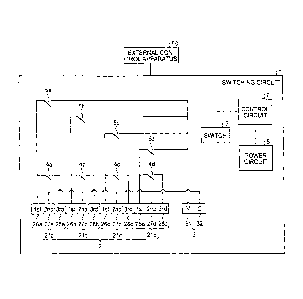
[0010] First Embodiment.
First, the configuration of a no-voltage output and
voltage output switching circuit 1 according to a first
embodiment will be described. FIG. 1 is a diagram
illustrating the configuration of the no-voltage output and
voltage output switching circuit 1 according to the first
embodiment. In the present application, a "no-voltage
output and voltage output switching circuit" is sometimes
referred to as a "switching circuit." The switching
circuit 1 includes an actuator connection terminal block 2.
The actuator connection terminal block 2 includes a port
21a, a port 21b, a port 21c, and a port 21d to which
actuators are connected. To describe FIG. 1 simply, the
actuators are not illustrated in FIG. 1.
[0011] The port 21a, the port 21b, the port 21c, and the
port 21d are an example of a plurality of ports. The port
21a, the port 21b, the port 21c, and the port 21d are each
independent from the other ports. The port 21a, the port
21b, the port 21c, and the port 21d may be formed
integrally. The port 21a, the port 21b, the port 21c, and
the port 21d may each be formed in a separated state from
the other ports.
[0012] The port 21a includes a first pin 26a, a second
pin 27a, and a third pin 28a. The port 21b includes a
first pin 26b, a second pin 27b, and a third pin 28b. The
port 21c includes a first pin 26c, a second pin 27c, and a
third pin 28c. The port 21d includes a first pin 26d, a
CA 03018538 2018-09-20
second pin 27d, and a third pin 28d. To each of the pins,
an actuator is connected.
[0013] The first pin 26b, the first pin 26c, and the
first pin 26d each include a function identical to that of
5 the first pin 26a. The second pin 27b, the second pin 27c,
and the second pin 27d each include a function identical to
that of the second pin 27a. The third pin 28b, the third
pin 28c, and the third pin 28d each include a function
identical to that of the third pin 28a. That is, the port
21b, the port 21c, and the port 21d each include a function
identical to that of the port 21a.
[0014] The switching circuit 1 further includes a power
connection terminal block 3. The power connection terminal
block 3 includes a voltage terminal 31 and a common
terminal 32 to which a power supply is connected. The
voltage terminal 31 is a terminal to which a voltage
different from a voltage applied to the common terminal 32
is applied when the power supply is connected to the power
connection terminal block 3. The common terminal 32 is
connected to the second pin 27a of the port 21a, the second
pin 27b of the port 21b, the second pin 27c of the port 21c,
and the second pin 27d of the port 21d individually.
[0015] The switching circuit 1 further includes a first
relay 4a, a first relay 4b, a first relay 4c, and a first
relay 4d. The first relay 4a, the first relay 4b, the
first relay 4c, and the first relay 4d are an example of a
plurality of first relays. The first relay 4a corresponds
to the port 21a, the first relay 4b corresponds to the port
21b, the first relay 4c corresponds to the port 21c, and
the first relay 4d corresponds to the port 21d.
[0016] The first relay 4b, the first relay 4c, and the
first relay 4d each include a function identical to that of
the first relay 4a. The first relay 4a, the first relay 4h,
CA 03018538 2018-09-20
6
the first relay 4c, and the first relay 4d are each a
normally open contact relay. The first relay 4a, the first
relay 4b, the first relay 4c, and the first relay 4d are
each a relay for supplying no-voltage output to an actuator
connected to a corresponding port.
[0017] The first relay 4a enables connection between the
first pin 26a of the corresponding port 21a and the third
pin 28a of the port 21a. The first relay 4b enables
connection between the first pin 26b of the corresponding
port 21b and the third pin 28b of the port 21b. The first
relay 4c enables connection between the first pin 26c of
the corresponding port 21c and the third pin 28c of the
port 21c. The first relay 4d enables connection between
the first pin 26d of the corresponding port 21d and the
third pin 28d of the port 21d.
[0018] The switching circuit 1 further includes a second
relay 5a, a second relay 5b, a second relay 5c, and a
second relay 5d. The second relay 5a, the second relay 5b,
the second relay 5c, and the second relay 5d are an example
of a plurality of second relays. The second relay 5a
corresponds to the port 21a, the second relay 5b
corresponds to the port 21b, the second relay 5c
corresponds to the port 21c, and the second relay 5d
corresponds to the port 21d.
[0019] That is, the second relay 5a corresponds to the
first relay 4a, the second relay 5b corresponds to the
first relay 4b, the second relay 5c corresponds to the
first relay 4c, and the second relay 5d corresponds to the
first relay 4d. The second relay 5b, the second relay Sc,
and the second relay 5d each include a function identical
to that of the second relay 5a. The second relay 5a, the
second relay 5b, the second relay Sc, and the second relay
5d are each a normally open contact relay. The second
CA 03018538 2018-09-20
7
relay 5a, the second relay 5b, the second relay 5c, and the
second relay 5d are each a relay for supplying voltage
output to an actuator connected to the corresponding port.
[0020] The second relay 5a enables connection between
the first pin 26a of the corresponding port 21a and the
voltage terminal 31. The second relay 5b enables
connection between the first pin 26b of the corresponding
port 21b and the voltage terminal 31. The second relay 5c
enables connection between the first pin 26c of the
corresponding port 21c and the voltage terminal 31. The
second relay 5d enables connection between the first pin
26d of the corresponding port 21d and the voltage terminal
31.
[0021] The switching circuit 1 further includes a switch
6 that allows a user to select either no-voltage output or
voltage output for the port 21a, the port 21b, the port 21c,
and the port 21d individually. FIG. 2 is a diagram
illustrating the configuration of the switch 6 of the no-
voltage output and voltage output switching circuit 1
according to the first embodiment. The switch 6 is a Dual
In-line Package (DIP) switch, for example. When the user
selects voltage output for the port 21a, the port 21b, the
port 21c, and the port 21d individually, "ON" on the switch
6 is selected by the user. When the user selects no-
voltage output, "OFF" on the switch 6 is selected by the
user. Shaded portions in FIG. 2 indicate that the shaded
portions are selected.
[0022] FIG. 2 illustrates a situation where on the
switch 6, "ON" corresponding to voltage output is selected
for the port 21a and the port 21c individually, and "OFF"
corresponding to no-voltage output is selected for the port
21b and the port 21d individually.
[0023] The switching circuit 1 further includes a
CA 03018538 2018-09-20
8
control circuit 7 that controls the first relay 4a, the
first relay 4b, the first relay 4c, the first relay 4d, the
second relay 5a, the second relay 5b, the second relay 5c,
and the second relay 5d individually. The control circuit
7 controls each of the plurality of first relays and the
plurality of second relays, according to a selection made
by the user using the switch 6. The control circuit 7
includes an integrated circuit for performing the control.
An example of the integrated circuit is a microcomputer.
[0024] Part or all of the functions of the control
circuit 7 may be implemented by a processing circuit 61.
FIG. 3 is a diagram illustrating the processing circuit 61
when at least a component of the control circuit 7 of the
no-voltage output and voltage output switching circuit 1
according to the first embodiment constitutes the
processing circuit 61. The processing circuit 61 is
dedicated hardware. Specifically, the processing circuit
61 is, for example, a single circuit, a combined circuit, a
programmed processor, a parallel-programmed processor, an
application-specific integrated circuit (ASIC), a field-
programmable gate array (FPGA), or a combination of them.
Part of the control circuit 7 may be dedicated hardware
separate from the remainder.
[0025] Part or all of the functions of the control
circuit 7 may be implemented by a processor 72 that
executes a program stored in a memory 71. FIG. 4 is a
diagram illustrating the processor 72 when at least a
component of the control circuit 7 of the no-voltage output
and voltage output switching circuit 1 according to the
first embodiment constitutes the processor 72. FIG. 4 also
illustrates the memory 71. The processor 72 is a central
processing unit (CPU), a processing unit, an arithmetic
unit, a microprocessor, a microcomputer, or a digital
CA 03018538 2018-09-20
9
signal processor (DSP).
[0026] When at least a component of the control circuit
7 constitutes the processor 72, the functions of the
component of the control circuit 7 are implemented by a
combination of the processor 72 and software, firmware, or
software and firmware. Software or firmware is described
as a program and stored in the memory 71. The processor 72
reads out and executes the program stored in the memory 71,
thereby implementing the functions of the component of the
control circuit 7.
[0027] That is, when at least a component of the control
circuit 7 constitutes the processor 72, the control circuit
7 includes the memory 71 for storing a program that results
in execution of steps executed by the component
constituting the control circuit 7. It can be said that
the program stored in the memory 71 causes a computer to
execute a process or method executed by the component of
the control circuit 7.
[0028] The memory 71 is, for example, nonvolatile or
volatile semiconductor memory such as random-access memory
(RAM), read-only memory (ROM), flash memory, an erasable
programmable read-only memory (EPROM), or an electrically
erasable programmable read-only memory (EEPROM), or a
magnetic disk, a flexible disk, an optical disk, a compact
disk, a mini disk, a digital versatile disk (DVD), or the
like.
[0029] Part of the functions of the control circuit 7
may be implemented by dedicated hardware, and the remainder
may be implemented by software or firmware. Thus, the
functions of the control circuit 7 can be implemented by
hardware, software, firmware, or a combination of them.
[0030] The switching circuit 1 further includes a power
circuit 8 that supplies power to the control circuit 7. An
CA 03018538 2018-09-20
external control apparatus 50 that controls the switching
circuit 1 and actuators connected to the switching circuit
1 is connected to the switching circuit 1. The external
control apparatus 50 may control the switching circuit 1
5 and the actuators by radio, or may control the switching
circuit 1 and the actuators by wire. The external control
apparatus 50 may be included in the switching circuit 1.
[0031] Next, a method of using the switching circuit 1
will be described. A user connects each of four actuators
10 to the port 21a, the port 21b, the port 21c, or the port
21d. The user is, for example, an operator who mounts
actuators to the switching circuit 1. To supply no-voltage
output to an actuator, the user connects the actuator to a
first pin and a third pin of a port. For example, to
supply no-voltage output to an actuator to be mounted to
the port 21a, the user connects the actuator to the first
pin 26a of the port 21a and the third pin 28a of the port
21a.
[0032] To supply voltage output to an actuator, the user
connects the actuator to a first pin and a second pin of a
port. For example, to supply voltage output to an actuator
to be mounted to the port 21a, the user connects the
actuator to the first pin 26a of the port 21a and the
second pin 27a of the port 21a.
[0033] Next, the user selects either no-voltage output
or voltage output for the port 21a, the port 21b, the port
21c, and the port 21d individually, using the switch 6.
For example, to supply voltage output to an actuator
mounted to the port 21a, the user selects "ON" on a portion
of the switch 6 corresponding to the port 21a as
illustrated in FIG. 2. For example, to supply no-voltage
output to an actuator mounted to the port 21b, the user
selects "OFF" on a portion of the switch 6 corresponding to
CA 03018538 2018-09-20
11
the port 21b as illustrated in FIG. 2.
[0034] The control circuit 7 controls on and off of each
of the plurality of first relays and the plurality of
second relays, according to a selection made by the user
using the switch 6. For example, when the user selects
"ON" for the port 21a, using the switch 6, the control
circuit 7 turns the first relay 4a off and turns the second
relay 5a on. For example, when the user selects "OFF" for
the port 21b, using the switch 6, the control circuit 7
turns the first relay 4b on and turns the second relay 5b
off.
[0035] As described above, the switching circuit 1 in
the first embodiment includes the port 21a, the port 21b,
the port 21c, and the port 21d each including the first pin,
the second pin, and the third pin. In addition, the
switching circuit 1 includes the first relay 4a, the first
relay 4b, the first relay 4c, and the first relay 4d. The
first relay 4a, the first relay 4b, the first relay 4c, and
the first relay 4d each enable connection between the first
pin of the corresponding port and the third pin of the
corresponding port. In other words, the first relay 4a,
the first relay 4b, the first relay 4c, and the first relay
4d each select no-voltage output when an actuator is
connected to the first pin and the third pin at the
corresponding port. That is, the first relay 4a, the first
relay 4b, the first relay 4c, and the first relay 4d each
allow supply of no-voltage output to an actuator when the
actuator is connected to the first pin and the third pin at
the corresponding port.
[0036] The switching circuit 1 further includes the
second relay 5a, the second relay 5b, the second relay Sc,
and the second relay 5d. The second relay 5a, the second
relay 5b, the second relay 5c, and the second relay 5d each
CA 03018538 2018-09-20
12
enable connection between the first pin of the
corresponding port and the voltage terminal 31 of the power
connection terminal block 3. The common terminal 32 of the
power connection terminal block 3 is connected to the
second pin of each port.
[0037] Thus, the second relay 5a, the second relay 5b,
the second relay 5c, and the second relay 5d each select
voltage output when an actuator is connected to the first
pin and the second pin at the corresponding port. That is,
the second relay 5a, the second relay 5b, the second relay
5c, and the second relay 5d each allow supply of voltage
output to an actuator when the actuator is connected to the
first pin and the second pin at the corresponding port.
[0038] As described above, the switching circuit 1 in
the first embodiment can supply no-voltage output to an
actuator when the actuator is connected to the first pin
and the third pin at each port, and can supply voltage
output to an actuator when the actuator is connected to the
first pin and the second pin. As described above, the port
21a, the port 21b, the port 21c, and the port 21d are each
independent from the other ports.
[0039] Thus, the switching circuit 1 allows independent
switching between no-voltage output and voltage output for
the port 21a, the port 21b, the port 21c, and the port 21d
individually. That is, the user can select no-voltage
output or voltage output for each port of the switching
circuit 1. As a result, the user can simultaneously
control a plurality of actuators corresponding to no-
voltage output or voltage output by using the switching
circuit 1.
[0040] As described with reference to FIG. 2, in the
above-described first embodiment, when the user selects
voltage output for the port 21a, the port 21b, the port 21c,
CA 03018538 2018-09-20
13
and the port 21d individually, "ON" on the switch 6 is
selected by the user, and when the user selects no-voltage
output, "OFF" on the switch 6 is selected by the user.
However, "ON" and "OFF" on the switch 6 may be set in an
opposite way to the above-described case. Specifically,
when the user selects voltage output for the port 21a, the
port 21b, the port 21c, and the port 21d individually,
"OFF" on the switch 6 may be selected by the user, and when
the user selects no-voltage output, "ON" on the switch 6
may be selected by the user.
[0041] On the switch 6 in FIG. 2, the position where
"ON" or "OFF" of the port 21a is selected is leftmost, and
the position where "ON" or "OFF" of the port 21d is
selected is rightmost. However, the positions where "ON"
or "OFF" of the port 21a, the port 21b, the port 21c, and
the port 21d is selected individually are not limited to
the positions illustrated in FIG. 2. For example, the
position where "ON" or "OFF" of the port 21a is selected
may be rightmost, and the position where "ON" or "OFF" of
the port 21d is selected may be leftmost.
[0042] When the user selects no-voltage output or
voltage output for the port 21a, the port 21b, the port 21c,
and the port 21d individually, the switch 6 is used in the
above-described first embodiment. A means for selecting
no-voltage output or voltage output may be a means
substituting for the switch 6. An example of the means
substituting for the switch 6 is a hardware switch.
[0043] Another example of the means substituting for the
switch 6 is jumpers provided to the port 21a, the port 21b,
the port 21c, and the port 21d individually. For example,
the user disconnects a jumper when selecting no-voltage
output, and keeps a connecting state of the jumper when
selecting voltage output. Alternatively, for example, the
CA 03018538 2018-09-20
14
user keeps a connecting state of a jumper when selecting
no-voltage output, and disconnects the jumper when
selecting voltage output.
[0044] Still another example of the means substituting
for the switch 6 is the external control apparatus 50.
Still another example of the means substituting for the
switch 6 is a control device that selects no-voltage output
or voltage output for the port 21a, the port 21b, the port
21c, and the port 21d individually upon receiving a user's
instruction. When the control device constitutes the means
substituting for the switch 6, an instruction received by
the control device is transmitted to the external control
apparatus 50 by wire or radio, and is provided to the
switching circuit 1 by the external control apparatus 50.
An example of the control device is a smartphone or a
tablet personal computer.
[0045] Still another example of the means substituting
for the switch 6 is a sensor that detects the state of the
air outside the switching circuit 1 and a control apparatus
that selects no-voltage output or voltage output for the
port 21a, the port 21b, the port 21c, and the port 21d
individually, based on information obtained by the sensor.
An example of the sensor is a humidity sensor or a
temperature sensor. The sensor is connected to the
switching circuit 1. The control apparatus selects no-
voltage output or voltage output for each port, based on a
preset rule for the sensor and information obtained by the
sensor. The control apparatus may be provided inside the
switching circuit 1, or may be provided outside the
switching circuit 1.
[0046] Second Embodiment.
FIG. 5 is a diagram illustrating the configuration of
a no-voltage output and voltage output switching circuit lA
CA 03018538 2018-09-20
according to a second embodiment. The switching circuit lA
in the second embodiment includes all the components of the
switching circuit 1 in the first embodiment. In the second
embodiment, differences from the first embodiment will be
5 described. The switching circuit lA further includes a
jumper 9a corresponding to the port 21a, a jumper 9b
corresponding to the port 21b, a jumper Sc corresponding to
the port 21c, and a jumper 9d corresponding to the port 21d.
[0047] The jumper 9a connects a connection point 10a
10 between the first relay 4a corresponding to the port 21a
and the second relay 5a corresponding to the port 21a, and
the first pin 26a of the corresponding port 21a. The
jumper 9b connects a connection point 10b between the first
relay 4b corresponding to the port 21b and the second relay
15 5b corresponding to the port 21b, and the first pin 26b of
the corresponding port 21b. The jumper Sc connects a
connection point 10c between the first relay 4c
corresponding to the port 21c and the second relay 5c
corresponding to the port 21c, and the first pin 26c of the
corresponding port 21c. The jumper 9d connects a
connection point 10d between the first relay 4d
corresponding to the port 21d and the second relay 5d
corresponding to the port 21d, and the first pin 26d of the
corresponding port 21d. The switching circuit lA in the
second embodiment has effects identical to the effects
obtained by the switching circuit 1 in the first embodiment.
[0048] Third Embodiment.
FIG. 6 is a diagram illustrating the configuration of
a no-voltage output and voltage output switching circuit 1B
according to a third embodiment. The switching circuit 1B
in the third embodiment includes all the components of the
switching circuit 1 in the first embodiment except the
first relay 4a, the first relay 4b, the first relay 4c, and
CA 03018538 2018-09-20
16
the first relay 4d. In the third embodiment, differences
from the first embodiment will be described.
[0049] The switching circuit 1B further includes a first
relay lla, a first relay 11b, a first relay 11c, and a
first relay 11d. The first relay 11a, the first relay 11b,
the first relay 11c, and the first relay lid are an example
of a plurality of first relays. The first relay ha
corresponds to the port 21a, the first relay llb
corresponds to the port 21b, the first relay 11c
corresponds to the port 21c, and the first relay lid
corresponds to the port 21d.
[0050] That is, the first relay ha corresponds to the
second relay 5a, the first relay llb corresponds to the
second relay 5b, the first relay 11c corresponds to the
second relay 5c, and the first relay lld corresponds to the
second relay 5d. The first relay 11b, the first relay 11c,
and the first relay lid each include a function identical
to that of the first relay lla. The first relay 11a, the
first relay 11b, the first relay 11c, and the first relay
lid are each a transfer contact relay.
[0051] The first relay ha connects the first pin 26a of
the port 21a and the second relay 5a, or connects the third
pin 28a of the port 21a and the second relay 5a. The first
relay lib connects the first pin 26b of the port 21b and
the second relay 5b, or connects the third pin 28b of the
port 21b and the second relay 5b. The first relay llc
connects the first pin 26c of the port 21c and the second
relay 5c, or connects the third pin 28c of the port 21c and
the second relay Sc. The first relay lid connects the
first pin 26d of the port 21d and the second relay 5d, or
connects the third pin 28d of the port 21d and the second
relay 5d.
[0052] In the third embodiment, the second relay 5a
CA 03018538 2018-09-20
17
enables connection between the corresponding first relay
ha and the voltage terminal 31, the second relay 5b
enables connection between the corresponding first relay
lib and the voltage terminal 31, the second relay 5c
enables connection between the corresponding first relay
11c and the voltage terminal 31, and the second relay 5d
enables connection between the corresponding first relay
lid and the voltage terminal 31. That is, by using the
switching circuit 1B in the third embodiment, a user can
control actuators corresponding to transfer contact relays.
[0053] Fourth Embodiment.
FIG. 7 is a diagram illustrating the configuration of
a no-voltage output and voltage output switching circuit 1C
according to a fourth embodiment. The switching circuit 1C
in the fourth embodiment includes all the components of the
switching circuit 1 in the first embodiment except the
first relay 4c. In the fourth embodiment, differences from
the first embodiment will be described.
[0054] The switching circuit 1C further includes the
jumper 9a corresponding to the port 21a, the jumper 9b
corresponding to the port 21b, and the first relay 11c
corresponding to the port 21c. The jumper 9a and the
jumper 9b are each the one described in the second
embodiment. The first relay 11c is the one described in
the third embodiment. In the switching circuit 1C, the
first relay 4d is an example of a first specific relay.
Each of the first relay 4a and the first relay 4h is also
an example of the first specific relay. In the switching
circuit 1C, the first relay 11c is an example of a second
specific relay.
[0055] For the port 21a, the port 21b, and the port 21d,
no-voltage output and voltage output can be switched, so
that by using the switching circuit 1C, actuators
CA 03018538 2018-09-20
18
corresponding to no-voltage output or voltage output can be
controlled. For the port 21c, by using the switching
circuit 1C, an actuator corresponding to a transfer contact
relay can be controlled. That is, by using the switching
circuit 1C, both an actuator corresponding to no-voltage
output or voltage output and an actuator corresponding to a
transfer contact relay can be controlled.
[0056] The control circuit 7 stores information that an
actuator corresponding to a transfer contact relay is
connected to the port 21c and the first relay 11c performs
the operation of a transfer contact relay.
[0057] The configurations described in the above
embodiments show an example of the content of the present
invention, and can be combined with another known art, and
can be partly omitted or changed without departing from the
scope of the present invention.
Reference Signs List
[0058] 1, 1A, 1B, 1C no-voltage output and voltage
output switching circuit; 2 actuator connection terminal
block; 3 power connection terminal block; 4a, 4b, 4c, 4d,
lla, 11b, 11c, lid first relay; 5a, 5b, Sc, 5d second
relay; 6 switch; 7 control circuit; 8 power circuit; 9a,
9b, 9c, 9d jumper; 10a, 10b, 10c, 10d connection point;
21a, 21b, 21c, 21d port; 26a, 26b, 26c, 26d first pin;
27a, 27b, 27c, 27d second pin; 28a, 28b, 28c, 28d third
pin; 31 voltage terminal; 32 common terminal; 50
external control apparatus; 61 processing circuit; 71
memory; 72 processor.