Note: Descriptions are shown in the official language in which they were submitted.
Lamp Strip
FIELD OF THE INVENTION
100011 The present invention relates to the field of lighting technology,
particularly to
a lamp strip.
BACKGROUND OF THE INVENTION
[0002] Because of its characteristics of soft, light, pure color and easy
installation,
LED lamp strips are widely used in decoration of building contours, steps,
booths,
bridges, hotels. KTV decorative lighting, advertising signs, advertising
designs for
animations, scripts and paintings, and so on. When using a flexible lamp
strip, it is
often necessary to adjust the length of the strip by cutting the strip to meet
different
requirements in various occasions, but the cutting may easily destroy the LED
inside
the lamp strip and affects the use. To facilitate the cutting, the lamp strip
is usually
accompanied with a cut mark, the cut mark is generally disposed on the side
facing
away from the light source, and the cut mark can be seen through a light-
transmitting
layer of the lamp strip for cutting.
[0003] Since the use of LED lamp strips is more and more widespread, there is
a need
for different shapes and colors of the strips. Currently, a cut mark is hardly
seen
through a light-transmitting layer in the condition that the lamp strip is not
transparent,
making it difficult for appropriate cutting of the lamp strip.
[0004] Chinese patent CN206669424U discloses a flexible LED lamp strip with a
cut
mark and an LED lamp strip easy for cutting, wherein the cut mark is set on
the side
of the circuit board of the LED lamp strip main body facing away from an LED
light
source, and the cut mark is further provided with light-transmitting holes, so
that the
light emitted by the LED light source on the other side of the lamp strip
passes
through the light-transmitting holes to the other side of the lamp strip, or
the light of
1
CA 3018742 2020-01-17
an external light source on one side passes through the light-transmitting
holes to the
other side of the lamp strip, thus a user can accurately locate the cutting
site,
preventing damages to the lamp strip by mis-operation and improving the
cutting
quality.
[0005] In the above-mentioned patent, the cut mark is set on the circuit board
of the
lamp strip, so the cut mark can only be seen when the lamp lights up or there
is an
external light source, which is inconvenient to use. In addition, the main
body of the
light strip needs to be provided with a light-transmitting layer of
observation, which
not only increases the production cost, but also causes light leak from the
light-transmitting layer of observation, thus reducing the luminous efficiency
of the
lamp strip.
[0006] Moreover, at present some LED lamp strips are provided with several LED
chips, the LED chips are all connected in series on a flexible lamp panel of
the LED
lamp strip. If one or some of the LED chips are damaged, the entire LED lamp
strip
will not work due to disconnection, and the entire lamp strip needs to be
repaired or
replaced which is inconvenient for users.
SUMMARY OF THE INVENTION
[0007] The technical problem to be solved by the present invention is to
provide a
lamp strip which is simple in structure, convenient for cutting, handy and
practical
with a prolonged service life, increased durability and few maintenance.
[0008] The technical problem to be solved by the present invention is to
provide a
lamp strip with uniform illumination and pleasing overall appearance.
[0009] The technical problem to be solved by the present invention is to
provide a
lamp strip which is convenient to install and produced in automation
[00010] To solve the above-mentioned technical problems, the present invention
provides an LED lamp strip which comprises an outer casing, an inner casing
installed
in the outer casing, and a light-emitting component disposed in the inner
casing. The
2
CA 3018742 2020-01-17
light-emitting component includes a substrate and several LED illuminant
modules set
on the substrate, each LED illuminant module is connected in parallel with
each other,
each LED illuminant module includes at least one LED light source. The inner
casing
is provided with a light exit through which the light from the LED light
source can
directly go out, a cut mark is provided between the light exits locating
between the
LED illuminant modules in parallel accordingly, and the surface of the outer
casing
facing the LED light source is of light transmission.
[00011] The LED illuminant modules also comprises a protection circuit, the
protection circuit is connected in parallel with at least one LED light
source, when the
LED light source is disconnected, the protection circuit is turned on to
maintain the
operation of the light-emitting component.
[00012] Preferably, the inner casing is provided with a cavity and a slot, the
slot is
located at a bottom of the inner casing and connects with the cavity, the
cavity is
attached to the light exit, and the light-emitting component is disposed in
the cavity
[00013] More preferably, the upper surface of the light-transmitting layer has
many
curved protrusions, and there are many small holes on the side towards the LED
light
source of the light-transmitting layer.
[00014] More preferably, the diameter of each curved protrusion is D, the
distance
between the peaks of two adjacent curved protrusions is R, the diameter of the
small
hole is d, and the distance between adjacent small holes is r, the distance
between the
LED light source and the curved protrusion is L, wherein
[00015] arctan(R-r) / f= arccos(D-d) / f.
[00016] More preferably, the light-emitting component further comprises two
conductive strips, the conductive strips are disposed on the substrate laying
on both
sides of the LED illuminant module, connecting every LED illuminous module in
parallel.
[00017] More preferably, the conductive strip is a copper wire or a copper
plate, the
conductive strip is fixed to the substrate by welding.
[00018] More preferably, the light-transmitting layer is melt-extruded by a
3
CA 3018742 2020-01-17
composition of at least two kinds of resins comprising a light diffusion layer
of a
ridge structure, the light diffusion layer has a thickness of 200 p.m to 400
p.m.
[00019] More preferably, the protection circuit includes a Zener diode that is
connected in anti-parallel with at least one LED light source, the Zener diode
has a
stabilized voltage greater than the terminal voltage when at least one LED
light source
connected in parallel with the Zener diode operates.
[00020] More preferably, the light-emitting component includes at least two
LED
illuminant modules, the LED illuminant module is composed of at least one LED
light
source, and the protection circuit comprises a regulated triode, and the A-
terminal of
the triode is respectively connected with a cathode of one LED light source
and an
anode of another LED light source, the B-terminal of the triode is connected
to an
anode of one LED light source, and the C-terminal of the triode is connected
to a
cathode of another LED light source.
[00021] More preferably, the light-emitting component also comprises a
current-limiting circuit which is connected in series with the LED light
source. The
present invention has the following beneficial effects:
[00022] 1. The LED lamp strip of the present invention has a simple structure,
a user
can see the cut mark on the inner casing through the light-transmitting layer
directly.
When setup, the user only needs to cut the lamp strip according to the cutting
mark to
use, since the cut mark is correspondingly arranged between the LED illuminant
modules in parallel, the circuit will not be affected, and thus the
illumination
guaranteed. The LED lamp strip also comprises a protection circuit, when one
or
some LED chips are damaged, the protection circuit replaces the damaged LED
chip
to conduct electricity, so that the lamp strip of the present invention can
continue to be
energized and illuminate which greatly extends the lifespan and durability of
the lamp
strip.
[00023] 2. The light-transmitting layer of the present invention adopts the
principle of
ommateum. Each curved protrusion serves as a microlens, and multiple curved
protrusions as a microlens array for luminous radiation. In addition, having
several
small holes on the side of the light-transmitting layer facing the LED light
source,
4
CA 3018742 2020-01-17
each small hole acts as a small eye of a compound eye being independent of
each
other, so that the light passing through the different small holes does not
interfere with
each other. The light-transmitting layer of the present invention radiates the
light
emitted by the LED light source, which thereby greatly improves the luminous
efficiency and uniformity of the lamp strip, makes the color of the light
emitted by the
lamp strip more uniform when projected onto the object and avoids
discoloration or
spotting of the light, thus providing a more pleasing overall appearance of
the lamp
strip.
[00024] The LED lamp strip provided by the present invention, wherein the
conductive strip is disposed on the substrate to form a parallel connection of
each
LED illuminant module, an external power is electrically connected with the
substrate,
and the conductive strip and the substrate are integrated structures which can
be
installed by equipment automatically making the installation labor-saving and
more
efficient.
BRIEF DESCRIPTION OF DRAWINGS
[00025] Figure 1 shows a structural schematic of an LED lamp strip of the
present
invention.
[00026] Figure 2 shows a stereoscopic exploded view of an LED lamp strip of
the
present invention.
[00027] Figure 3 shows a structural schematic of a light-emitting component
installed
in an inner casing of the present invention.
[00028] Figure 4 shows a circuit diagram of an LED lamp strip of the present
invention.
[00029] Figure 5 shows a schematic of an inner casing and a light-emitting
component according to one embodiment of the present invention.
[00030] Figure 6 shows a structural schematic of a light-emitting component
according to one embodiment of the present invention.
CA 3018742 2020-01-17
DETAILED DESCRIPTION OF ILLUSTRATED EMBODIMENTS
[00031] To better illustrate the present invention in aspects of the
objective, technical
scheme and advantages, the present invention is further described in detail
with
reference to the accompanying drawings
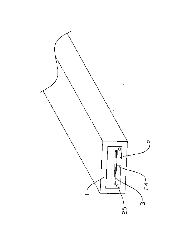
[00032] Referring to FIG. 1 to FIG. 3, the present invention provided an LED
lamp
strip which comprised an outer casing 1, an inner casing 2 installed in the
outer casing
1, and a light-emitting component 3 disposed in the inner casing 2. The light-
emitting
component 3 included a substrate 31 and several LED illuminant modules fixed
on
the substrate 31, each LED illuminant module was connected in parallel with
each
other, each LED illuminant module included at least one LED light source 32.
The
inner casing 2 is provided with a light exit 21 through which the light from
the LED
light source 32 can directly go out, and the light exit 21 is provided with a
cut mark
22 laying between the LED illuminant modules in parallel, the surface of the
outer
casing 1 facing the LED light source 32 is of light transmission.
[00033] Specifically, the inner casing 2 was provided with a cavity 23 and a
slot 24,
and the slot 24 was located at the bottom of the inner casing 2 and connected
with the
cavity 23, the cavity 23 was attached to the light exit 21, and the light-
emitting
component 3 was disposed in the cavity 23. The present invention expanded the
volume of the cavity 23 by the use of slot 24, thereby facilitating the
placement of the
substrate 31 into the cavity 23 and insertion of the LED light source 32 into
the light
exit 21. According to the prior art, the inner casing of the lamp strip has at
least one
transparent side, and since the LED light source is disposed in the inner
casing, the
light emitted from the LED light source needs to go through the inner casing.
However, in the present invention the light from the LED light source emitted
out of
the outer casing directly through the light exit without passing through the
inner
casing, therefore, the inner casing of the present invention could be designed
in a
variety of colors. What's more, the opaque inner casing could also shield the
substrate,
6
CA 3018742 2020-01-17
that makes the lamp strip more pleasing to the eye and broaden its
application.
[00034] Further, the inner casing 2 was provided with two wire slots 25
additionally,
and the wire slots 25 were provided with wires electrically connected to the
substrate
31, and the wires formed a parallel connection for each LED illuminant module.
The
wire slots 25 were located below the cavity 23 and symmetrically disposed.
Moreover,
the wires were used to form an electrical connection between the external
power and
the substrate 31.
[00035] Specifically, the substrate 31 was a flexible circuit board, the
substrate 31
was provided with several LED light sources 32, and the LED light sources 32
were
convex on the substrate 31 and arranged in a row. The inner casing 2 was
encapsulated by the injection molding wrapping the substrate 31 inside, and
the LED
light source 32 protruded from the light exit 21 or in the light exit 21, and
the light
from the LED light source 32 directly emitted through the light-transmitting
layer of
the outer casing 1 without passing through the inner casing 2, thereby
improving the
luminous efficiency of the lamp strip. The cut mark 22 was formed when the
inner
casing 2 was injection molded, or made after the inner casing 2 was formed,
the cut
mark 22 could be disposed on the surface of the inner casing 2 or along the
inner
casing 2. Further, the shape of the cut mark 22 could be a circle, a triangle,
an ellipse,
a star, a polygon, a line, or the like.
[00036] The LED lamp strip of the present invention had a simple structure,
when
setup, the user only needs to cut according to the cutting mark for use, since
the cut
mark is correspondingly arranged between the LED illuminant modules in
parallel,
the circuit will not be affected by the cutting, and thus the illumination
guaranteed. In
addition, the LED illuminant module of the present invention was equipped with
a
Zener diode for stabilizing the voltage of the LED illuminant module and
ensuring
that the lamp strip do work after being cut.
1000371Since the light emitted by the LED light source 32 needs to pass
through the
light-transmitting layer, in order to improve the light uniformity of the LED
lamp strip,
the light-transmitting layer was melt-extruded by a composition of at least
two kinds
of resins comprising a light diffusion layer of a ridge structure, the light
diffusion
7
CA 3018742 2020-01-17
layer had a thickness of 200 um to 400 gm.
1000381Preferably, the refractivity difference of at least two resins was from
0.01 to
0.06.
[000391Preferably, at least two resins were incompatible, and at least one of
the resins
was a polyolefin-based resin, wherein the polyolefin-based resin was a
polyethylene-based resin, a polypropylene-based resin, or a cyclic polyolefin-
based
resin.
[000401Preferably, at least two resins were incompatible, wherein two of the
resins
was polyolefin-based resins, and the polyolefin-based resin was a polyethylene-
based
resin, a polypropylene-based resin, or a cyclic polyolefin-based resin.
10004111n order to increase the transmittance of the light-transmitting layer
of the
outer casing 1, the light was concentrated on the surface to prevent light
leakage from
side walls of the lamp strip, and lateral sides of the outer casing 1 are
opaque made of
an opaque material.
[000421As shown in FIG. 4, the present invention comprised a protection
circuit 4
that was connected in parallel with at least one LED light source 32, when the
LED
light source 32 was disconnected, the protection circuit 4 was turned on to
maintain
the operation of the substrate. That is, when one or some of the LED light
sources 32
on the lamp strip was damaged, the protection circuit 4 replaced the damaged
LED
light sources 32 to conduct electricity, so that the lamp strip of the present
invention
could continue to be energized and illuminate which greatly extended the
lifespan and
durability of the lamp strip.
[00043]The protection circuit 4 of an embodiment, as shown in FIG. 4, included
at
least one Zener diode 5 that was connected in anti-parallel with at least one
LED light
source 32, the Zener diode 5 had a stabilized voltage greater than the
terminal voltage
when at least one LED light source 32 connected in parallel with the Zener
diode 5
operated. There were two Zener diodes 5 in FIG. 4, as the length of the lamp
strip
increases, there could be more Zener diodes 5. Each Zener diode 5 was in anti-
parallel
connection with three LED light sources 32, the regulated voltage of the Zener
diode
8
CA 3018742 2020-01-17
is Ud, the terminal voltage of the three LED light sources 32 is Ua, and Ud
was
slightly larger than Ua. Since Ua was smaller than Ud, the Zener diode 5 was
in a
non-conducting state, when any LED light source 32 was damaged, the circuit in
parallel with the Zener diode 5 was in an open state, at the instant of
opening, the
voltage of the Zener diode 5 was equal to the mains voltage, because the mains
voltage was larger than the regulated voltage Ud of the Zener diode 5, the
Zener diode
5 was turned on in reverse, the Zener diodes 5 and the remaining LED light
sources
32 were then connected in series to form a loop, and the remaining LED light
sources
32 were still functional, thus the maintenance frequency reduced and the
durability
increased.
10004411n addition, the present invention further comprised a current-limiting
circuit
(see FIG. 4), the current-limiting circuit was connected in series with the
LED light
source 32, here, the current-limiting circuit was a current limiting resistor,
and the
current limiting resistor could reduce the current flowing went through the
LED light
source 32 to ensure the LED light source 32 operated safely and steadily.
1000451In another preferable embodiment of the present invention, as shown in
FIG. 5,
the upper surface of the light-transmitting surface of the present invention
had many
curved protrusions 26, and there were many small holes 27 on the side towards
the
LED light source 32. Specifically, the diameter of each curved protrusion 26
was D,
the distance between the peaks of two adjacent curved protrusions 26 was R,
the
diameter of the small hole 27 was d, and the distance between adjacent small
holes 12
was r, the distance between the LED light source 32 and the curved protrusion
26 was
L, wherein arctan(R-r)/f= arccos (D-d)/f. The light-transmitting layer of the
preferable
embodiment adopted the principle of ommateum. Each curved protrusion served as
a
microlens, and several curved protrusions as a microlens array for luminous
radiation.
In addition, having several small holes on the side of the light-transmitting
layer
facing the LED light source 32, each small hole acted as a small eye of a
compound
eye being independent of each other, so that the light passing through the
different
small holes did not interfere with each other. The light-transmitting layer of
the
9
CA 3018742 2020-01-17
present invention radiated the light emitted by the LED light source 32, which
thereby
greatly improved the luminous efficiency and uniformity of the lamp strip,
made the
color of the light emitted by the lamp strip more uniform when projected onto
the
object and avoided discoloration or spotting of the light, providing a more
pleasing
overall appearance of the lamp strip.
10004611n another preferable embodiment of the present invention, as shown in
FIG. 6,
the light-emitting component 3 further included two conductive strips 33
disposed on
the substrate 31 laying on both sides of the LED illuminant module, connecting
every
LED illuminous module in parallel. The conductive strip 33 was a copper wire
or a
copper plate, but not limited thereto. In the present invention, the
conductive strip 33
could also be made of other conductive metals. The conductive strip 33 was
fixed to
the substrate 31 by welding, together with the substrate 31 as an integral
structure.
When setup, it is only necessary to mount the substrate 31 in the inner casing
2, while
the previous method requires manual insertion of the copper wire into the
inner casing
2 to form an electrically conductive connection with the substrate 31 which is
inefficient in production. Further, the conductive strips33 was used to form
an
electrical connection between the external power and the substrate 31.
[000471The above disclosures are only preferable embodiments of the present
invention, the scope of the present invention is not limited thereto, and thus
equivalent
amendments made in the claims of the present invention are still within the
scope of
the present invention.
CA 3018742 2020-01-17