Note: Descriptions are shown in the official language in which they were submitted.
84495303
1
High Voltage direct Current Energy Transmission (HVDCT) Air-
Core Inductor and Method for Manufacturing the HVDCT Air-Core
Inductor
Field of the Invention
The invention relates in general to the technical field of
transmitting electrical energy via high direct voltage, in
particular an High Voltage direct Current Energy Transmission
(HVDCT) air-core inductor and a method for manufacturing HVDCT
air-core inductor.
Background of the Invention
For the transmission of electrical energy at high power, from
about 1000 MW upwards, the transmission capacity has a limiting
effect over a particular line length since the reactive power
barely permits economical operation. In this power range, "high
voltage direct current energy transmission" systems (HVDCT)
have long been in use in a variety of application fields.
Components of such an HVDCT system can be, for example, HVDCT
smoothing reactors or HVDCT filter chokes. These components are
typically at a very high electrical potential relative to
earth, for example 500-800 kV. Typically, these components are
arranged outside. As a result, they are exposed to the
environmental conditions prevailing there, such as rain water
and dirt. Depending upon the environment, dirt particles can
become deposited on the outer surface of such an HVDCT
component and, with an irregular accumulation, can lead to a
distortion of the electric field along a component. A partial
discharging can occur on the HVDCT component. Ions can arise
CA 3019271 2018-10-30
84495303
2
which in turn act attractively on ionized and polarized
particles in the direct vicinity. At the exterior layer of the
coil of such an HVDCT smoothing reactor or filter choke, with
these particles an electric charge with opposite polarity is
built up, which either flows away to the terminals or
dissipates by discharging on the surface of the coil and
accumulates there. The at least partially electrically
conductive structure thereby arising at the surface of such an
HVDCT component can impair the operational behavior. In the
literature, this is referred to with the expression "black spot
phenomenon". The conductive structure that forms on the surface
of the HVDCT component can lead to an electric flashover. In
the worst case, the "black spot phenomenon" can, for example,
result in a total failure of an HVDCT smoothing reactor or
HVDCT filter choke.
In order to counteract this undesirable electrostatic
contamination, EP 2 266 122 El describes an electrostatic
shielding for an HVDCT component which is made of a covering
with a foil made of electrostatically dissipative material
having a surface resistance in the range of 109 to 1014
ohm/square. The covering is electrically connected to a
terminal of the HVDCT component. With such a semiconducting
foil on the outer surface of the coil, it is possible to
conduct charge carriers away from the surface of the component
and thus to prevent an electrostatic charging of the component
with the aforementioned negative consequences. In order to be
able to apply semiconducting foil to the coil, the substrate
must previously be prepared for a procedure of gluing the foil.
This can take place, for example, via a "dummy package" in that
the outermost layer of the coil of the HVDCT component is
CA 3019271 2018-10-30
64495303
3
initially wound round with a textile blended fabric band.
Subsequently, the blended fabric band is soaked or impregnated
with epoxy resin. Following the curing of the epoxy resin, a
polyurethane paint is sprayed on. This polyurethane paint is
roughened to prepare the adhesion surface. Subsequently, the
foil coated with a semiconducting layer is glued onto the
roughened polyurethane paint surface. In a last process step, a
cover layer is applied for protection. The material for this
cover layer can be a silicone that cross-links at room
temperature. The construction of such a "dummy package" thus
consists of a plurality of layers. The manufacturing is
complex. However, the application of the blended fabric band is
both a labor-intensive and a material-intensive process step.
Secondly, the self-adhesive foil is expensive because the foil
must withstand ultraviolet radiation over a long operating
life. The roughening of the paint surface that is required for
the gluing process is also labor-intensive and additionally
causes dust that is hazardous to health.
In view of the foregoing, there is therefore a need for an
HVDCT air-core inductor that is resistant to the "black spot
phenomenon- and is also producible simply and economically.
Summary of the Invention
It is an object of the present invention to provide a high
voltage direct current energy transmission (HVDCT) air-core
inductor and a method for its production that is constructed as
simply as possible and is economic to produce.
CA 3019271 2018-10-30
34495303
4
This and other objects and advantages are achieved in
accordance with the invention by an HVDCT air-core inductor and
for method, where in accordance with a fundamental concept of
the invention, in an HVDCT component, the formation of an
electrostatic screening is achieved not by gluing a foil, but
by applying a semiconducting lacquer onto the lateral surface
of an outer winding layer. This application occurs via a
spraying process. Through the spraying process, a surface film
is sprayed onto the coil surface, the electrical conduction
property of which corresponds substantially to the previously
used foil. In other words, the "dissipative" material
properties of the semiconducting layer manufactured in EP 2 266
122 B1 by gluing a semiconducting layer produced as a foil is
now achieved with a semiconducting layer manufactred by
spraying. This spray coatino now provides for the conduction
away of charge carriers that form during operation on the
surface of the HVDCT component. As a result, an electrostatic
charging of the component is thereby also effectively
counteracted. The great advantage lies in the more economical
production and the evenness of the screening effect.
In accordance with the invention, an HVDCT air-core inductor
therefore has a coating for the purpose of electrostatic
screening, which has been formed by atomization of a material,
i.e., a semiconducting paint. In that this semiconducting layer
is "sprayed" directly onto the surface of the coil conductor,
the "black spot phenomenon" can be very simply and effectively
counteracted. During the manufacturing, many cost-intensive
process steps can be dispensed with. That is, an expensive UV
stabilized, self-adhesive foil is dispensed with. Thus, a
complex surface treatment that is necessary for the glue-
CA 3019271 2018-10-30
84495303
connection of the foil is also dispensed with. The labor-
intensive application of a textile blended fabric band as a
substrate for gluing is also no longer required. The coating
surface is no longer roughened. Consequently, no grinding dust
5 also arises which could be hazardous to health.
It is particularly advantageous that the layer for
electrostatic screening can be produced. very simply, evenly,
and therefore economically. In contrast to the previously
required foil, with spray coating, there is no abutment site or
overlap of a semiconducting layer. The conducting away effect
is the same over the entire surface. Fewer process steps are
required during the manufacturing. Overall, the manufacturing
process is more economical.
It has been found that with an evenly applied screening layer
that has a thickness of approximately 80 pm to 120 pm, the
-blduk bpot phenomenon" can be efficiently counteracted. Such a
screening layer can be produced easily and with little cost
through spray coating.
The electrical property of this semiconducting layer can be
pre-set by suitable filler materials, i.e., conductive
particles, within broad limits. Conductive particles can be
formed via dielectric, platelet-shaped substrates that are each
covered by an electrically conductive layer. Suitable materials
for a substrate are, for example, natural or synthetic mica,
aluminum oxide, silicon oxide or glass, or mixtures thereof.
The electrically conductive layer of a particle can consist of
a doped metal oxide.
11
CA 3019271 2018-10-30
B4495303
6
With regard to low manufacturing costs, it can be favorable if
the material atomized in the spraying procedure is a polymer
with embedded semiconducting filler materials. An epoxy resin
or a polyurethane or a silicone or a polyester are suitable as
the polymer.
Preferable is a filler material which is formed of a metal
oxide or a silicon carbide.
Advantageously, the filler material is a doped metal oxide or a
doped silicon carbide.
A filler material has been found to be particularly preferable
which is composed proportionally of particles of undoped
silicon carbide and particles of a tin oxide doped with
antimony.
It is also an object of the invention to providc a method that
solves the problem set out in the introduction, i.e., a method
for manufacturing a component for an HVDCT exterior
installation where, on the externally arranged lateral surface
of an exterior winding layer, a semiconducting layer is applied
directly via an injection or spraying method. With this,
conventionally required process steps can be dispensed with,
such that the manufacturing costs are comparatively lower.
The method in accordance with the invention for producing an
HVDCT air-core inductor is characterized in that in a first
method step, a concentric winding arrangement is provided and
subsequently, the outer lateral surface of the winding
arrangement is formed coated with a spray coating method in
CA 3019271 2018-10-30
84495303
V
which a layer of a semiconducting paint formed from an
electrostatically dissipative material having a surface
resistance in the region from 109 to 1014 ohm/square is applied.
Particularly advantageously, for this spray coating method, the
so-called "high volume low pressure" (HVLP) method is used. With
this low pressure spraying method, a rapid and efficient
painting of large areas is possible. The atomization occurs due
to compressed air at a pressure of 3-4 bar. It is advantageous
herein that comparatively little spray mist is created. The
manufacturing method is therefore environmentally favorable.
According to one aspect of the present invention, there is
provided a high voltage direct current energy transmission
(HVDCT) air-core inductor, comprising: at least one concentric
winding layer having electrical terminals formed at ends
thereof; an electrostatic screen, comprising an outermost layer
made of electrostatically dissipative material which has a
surface resistance in a region of 109 to 1014 ohm/square, the
outermost electrostatically dissipative layer being provided at
least at one end with a collector electrode extending over a
periphery of the outermost electrostatically dissipative layer
for connection at one terminal of the electrical terminals;
wherein the outermost electrostatically dissipative layer is
formed as a continuous circumferentially arranged coating
disposed along a longitudinal axis of the air-core inductor,
said coating having no abutment site or circumferential overlap
on a lateral surface of an externally arranged winding layer.
Date Regue/Date Received 2022-12-09
84495303
8
According to another aspect of the present invention, there is
provided a method for producing a high voltage direct current
energy transmission (HVDCT) air-core inductor, comprising:
providing at least one concentric winding layer; and coating the
at least one concentric winding layer on an outer lateral
surface of the at least one concentric winding layer via a spray
coating method in which an outermost layer made of a
semiconducting paint which is formed from an outermost
electrostatically dissipative material having a surface
resistance in a region from 109 to 1014 ohm/square, wherein the
outermost layer is formed as a continuous circumferentially
arranged coating disposed along a longitudinal axis of the air-
core inductor, said coating have no abutment site or
circumferential overlap on the outer lateral surface of the at
least one concentric winding layer.
Other objects and features of the present invention will become
apparent from the following detailed description considered in
conjunction with the accompanying drawings. It is to be
understood, however, that the drawings are designed solely for
purposes of illustration and not as a definition of the limits
of the invention, for which reference should be made to the
appended claims. It should be further understood that the
drawings are not necessarily drawn to scale and that, unless
otherwise indicated, they are merely intended to conceptually
illustrate the structures and procedures described herein.
Date Regue/Date Received 2022-12-09
84495303
8a
Brief Description of the Drawings
For the further explanation of the invention, in the following
part of the description, reference is made to drawings in which
advantageous embodiments, details and developments of the
invention are disclosed on the basis of a non-restrictive
exemplary embodiment, in which:
Figure 1 is an HVDCT air-core inductor in accordance with the
invention in a side view;
Figure 2 is a detail representation taken from Figure 1 with a
view of the upper end side of the HVDCT air-core
inductor, such that a part of the winding arrangement
is seen in a perspective illustration;
Date Regue/Date Received 2022-12-09
B4495303
9
Figure 3 is the electrostatic screening of the HVDCT air-core
inductor of Figure 1 in a perspective view;
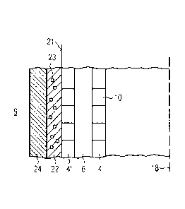
Figure 4 is a sectional representation through the winding
arrangement of Figure 2, wherein the layered structure
on the outer winding layer is shown enlarged; and
Figure 5 is a flowchart of the method in accordance with the
invention.
Detailed Description
Figure 1 shows an HVDCT air-core inductor 1 such as those
typically used for high voltage direct current transmission
(HVDCT) as smoothing reactors. The operation of such an HVDCT
air-core inductor 1 typically occurs outside, and it is
therefore also exposed to the prevailing outdoor weather
conditions. Thc drawing in Figure 1 shows the air-core inductor
1 in a vertically arranged position that is supported by
insulators 13 and a steel construction 15 on a base or on the
ground 15.
During operation, the air-core inductor 1 is at a high
electrical potential relative to earth, for example, 500-800 kV
and carries a current of up to 4000 A. The voltage drop across
the air-core inductor 1, i.e., between the electrical
connections 11 and 12 is lower in comparison thereto and
corresponds approximately to the residual ripple of the voltage
to be smoothed, typically approximately 100 V up to a few kV.
Only in the event of transient events, such as switching
processes or a lightning strike, can there be a significant
CA 3019271 2018-10-30
84495303
voltage drop across the air-core inductor 1 itself, which the
insulation of its windings must be able to withstand.
As shown in Figure 2, the air-core inductor 1 comprises an
5 electrical winding arrangement with a coil conductor 10 wound
helically about the axis 18. The individual layers 2, 3, 4 and
4' of the conductor 10 are held at a radial spacing by a spider
7, 8. Provided at each end, on each spider 7, 8, is a screening
cap 16 so that the action of points effect is reduced.
Due to the high electrical potential of the air-core inductor
1, a strong electrostatic field forms between the exterior of
the air-core inductor 1 and the ground 15. This potential can
lead to charge carriers from the surroundings 9 forming on the
lateral surface of the choke 1 with the consequences, as set
out in the introduction, of an electrostatic contamination or
the formation of "black spots". In order to counteract this
"black apoL phenomenon", the air-core inductor 1 is provided
with an electrostatic screening. This electrostatic screening
has conventionally been realized with a self-adhesive
semiconducting foil which, however, is now replaced in
accordance with the invention with a layer 22 that is sprayed
directly onto the outer winding layer and is described in
detail below.
Figure 2 shows a detailed view taken from Figure 1, looking
toward the upper end side of the HVDCT air-core inductor, so
that a part of the winding arrangement is visible in a spatial
representation. The semiconducting layer 22 is sprayed onto the
outer lateral surface 21 in the form of a paint coating (see
also Figure 4). It is evident from Figure 2 that the individual
CA 3019271 2018-10-30
84495303
11
winding layers 2, 3, 4, 4' of the air-core inductor 1 are
separated from one another by air gaps 6. The spider 7 holds
these winding layers 2, 3, 4, 4' at a spacing. Spacers 5 define
the spacing of the individual winding layers 2, 3, 4, 4' from
one another. At the end side, the spiders 7 are provided with a
screening cap 16.
Figure 3 shows the electrostatic screening 17 of the HVDCT air-
core inductor separately therefrom. The electrostatic screening
17 consists substantially of the hollow cylindrical layer 22
and at the end side, collector electrodes 19, 20 encircling the
circumference. The layer 22 was/is manufactured by spraying.
Using a spray pistol, a semiconducting polyurethane paint
was/is atomized in a spray pistol and sprayed at an air
pressure of 3-4 bar externally onto the lateral surface of the
winding layer 4'. During the spraying process, the spacing
between the spray pistol axis 18 and the coil 1 was/is kept
constant. In this way, with an automated spraying apparatus, an
electrically semiconducting coating 22 with an even layer
thickness of 80-120 pm can be created on the outer
circumferential surface of the winding layer 4'.
The coating 22 has collector electrodes 19, 20 on the end side,
each extending around the circumference. These collector
electrodes 19, 20 are conductively connected to the electrical
terminals 11, 12 of the air-core inductor 1.
The semiconducting layer 22 comprises a polymer substance that
contains a filler material, in the form of electric
semiconducting solid particles or pigments that are embedded in
the polymer material. The electric conductivity of the
CA 3019271 2018-10-30
84495303
12
particles can be varied within broad limits by doping their
material. Through doping or bringing together particles and
matrix material, a resistive coating 22 with a surface
resistance in a range between 109 and 1014 ohm/square can be
made. The layer 22 acts, as mentioned, as electrostatic
screening. With the electrically semiconducting layer 22, it is
achieved that the charge carriers impinging upon the air-core
inductor 1 from the exterior 9 pass "dissipativelY" by the
shortest route to the nearest collector electrode 19 or 20 and
from there are conducted away to one of the terminals 11 or 12.
By conducting away these charge carriers, the risk of the
formation of a conductive structure on the exterior of the air
gap choke 2 and therefore of a surface leakage current is
lessened. The disadvantages mentioned in the introduction can
thus be largely prevented.
Figure 4 shows a sectional representation through the winding
arrangement of FiguLe 2, where the layered structure on the
outer winding layer 4' is shown enlarged. The lateral surface
21 of the outer winding layer 4' is coated with the
semiconducting spray coating 22. The spray coating 22 contains
a filler material. In Figure 4, particles of the filler
material are identified with the reference character 23. The
filler material is composed of particles 23 of different
materials. In the present exemplary embodiment, the composition
of the filler material consists of a mixture of particles 23 of
different materials formed from undoped silicon carbide and
with antimony-doped tin oxide. Toward the exterior environment
9, the spray coating 22 is covered with a protective or
covering layer 24 which consists of an RTV silicone.
CA 3019271 2018-10-30
84495303
13
Figure 5 is a flowchart of a method for producing a high
voltage direct current energy transmission (HVDCT), air-core
inductor. The method comprises providing at least one
concentric winding layer 2, 3, 4, as indicated in step 510.
Next, the at least one concentric winding layer is coated on an
outer lateral surface 21 via a spray coating method in which a
layer 22 made of a semiconducting paint that is formed from an
electrostatically dissipative material having a surface
resistance in a region from 109 to 1014 ohm/square, as
indicated in step 520.
Although the invention has been described and explained in
detail on the basis of the two exemplary embodiments set out
above, the invention is not restricted to these examples. Other
embodiments and variations are conceivable without departing
from the underlying concept of the invention.
Thus, while there have been shown, described and pointed out
fundamental novel features of the invention as applied to a
preferred embodiment thereof, it will be understood that
various omissions and substitutions and changes in the form and
details of the devices illustrated, and in their operation, may
be made by those skilled in the art without departing from the
spirit of the invention. For example, it is expressly intended
that all combinations of those elements and/or method steps
which perform substantially the same function in substantially
the same way to achieve the same results are within the scope
of the invention. Moreover, it should be recognized that
structures and/or elements shown and/or described in connection
with any disclosed form or embodiment of the invention may be
CA 3019271 2018-10-30
34495303
14
incorporated in any other disclosed or described or suggested
form or embodiment as a general matter of design choice. It is
the intention, therefore, to be limited only as indicated by
the scope of the claims appended hereto.
CA 3019271 2018-10-30