Note: Descriptions are shown in the official language in which they were submitted.
CA 03020254 2018-10-05
DESCRIPTION
Title: LASER LIGHT SOURCE DEVICE
Technical Field
[0001] The present invention relates to a laser light source device,
particularly to a
technique to stably control a wavelength.
Background Art
[0002] A wavelength of laser light emitted from a semiconductor laser element
changes in accordance with a temperature of the semiconductor laser element.
Accordingly, a laser light source device of the related art that uses the
semiconductor
laser element as a light source for video equipment is provided with a
wavelength control
unit to obtain a desired wavelength. The wavelength control unit includes, for
example,
a temperature control unit using a ThermoElectric Cooler (TEC) such as Peltier
element
and a wavelength measuring unit that measures a wavelength of laser light (see
Patent
Document 1 and Non Patent Document 1).
Prior Art Documents
Patent Documents
[0003] Patent Document 1: Japanese Patent Application Laid-Open No. 2012-
124287
Non-Patent Documents
[0004] Non-Patent Document 1: Shota Yamamoto, "Wavelength Stabilization System
for Semiconductor Laser," Kochi University of Technology (March 2007),
[Online]
Internet (URL: http://www.kochi-
tech.acjp/library/ron/2006/2006ele/1070347.pdt)
searched on May 25th 2016
CA 03020254 2018-10-05
2
Summary
Problem to be Solved by the Invention
[0005] Temperature control using TEC requires a temperature sensor such as a
thermocouple and a temperature measuring resistor to measure a temperature of
a
semiconductor laser element. However, when the temperature sensor falls off
from the
temperature measuring unit, or a breakdown of the temperature sensor per se
occurs, a
problem is caused that temperature control is inappropriately performed.
Further, in a
temperature control system using TEC, temperatures of TEC and a surrounding
part
thereof are required to change to a target temperature, a thermal capacity
required for the
temperature control becomes large and responsiveness in the wavelength control
is low.
Moreover, in a temperature control system using TEC, the power is being
consumed
throughout the temperature control, and a problem of large power consumption
is further
caused.
[0006] It is an object of the present invention to provide a laser light
source device
stably operating, stably emitting laser light having a predetermined
wavelength, and
ensuring lower power consumption than that of the related art.
Means to Solve the Problem
[0007] According to an aspect of the present invention, a laser light source
device
includes a semiconductor laser element configured to emit laser light, a heat
radiation part
provided on a side of one surface of the semiconductor laser element, a heat
conductive
part having heat conductive characteristics, provided in contact with the one
surface of
the semiconductor laser element and the heat radiation part, configured to
conduct heat
generated in the semiconductor laser element to the heat radiation part, a
wavelength
CA 03020254 2018-10-05
3
measuring part configured to measure a wavelength of the laser light, and a
heat
conductive characteristic control part configured to change the heat
conductive
characteristics of the heat conductive part based on the wavelength of the
laser light
measured by the wavelength measuring part, and control the wavelength of the
laser light
to fall within a predetermined wavelength range.
Effects of the Invention
[0008] A laser light source device stably operating, stably emitting laser
light having a
predetermined wavelength, and ensuring lower power consumption than those of
the
related art is provided.
[0009] Those and other objects, features, aspects and advantages of the
present
invention will become more apparent from the following detailed description of
the
present invention will become more apparent from the following detailed
description of
the present invention when taken in conjunction with the accompanying
drawings..
Brief Description of Drawings
[0010] [FIG. 1] A diagram illustrating a configuration of a laser light
source device
according to an embodiment.
[FIG. 2] A block diagram for the laser light source device according to the
embodiment.
[FIG. 3] A diagram illustrating a processing circuit according to the
embodiment.
[FIG. 4] A diagram illustrating a processing circuit according to the
embodiment.
[FIG. 5] A diagram illustrating a state of a heat conductive part by stress
control
CA 03020254 2018-10-05
4
according to the embodiment.
[FIG. 6] A flowchart illustrating a wavelength control operation by heat
conductive characteristic control according to the embodiment.
[FIG. 7] A flowchart illustrating a stress control operation according to the
embodiment.
Description of Embodiment
[0011] An embodiment of a laser light source device according to the present
invention
is described.
[0012] (Configuration of Laser Light Source Device)
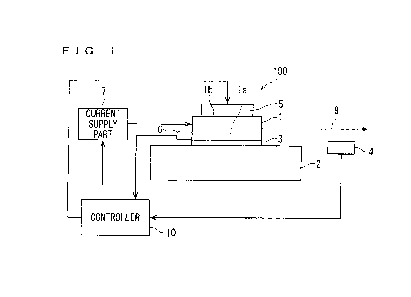
FIG. 1 is a diagram illustrating a configuration of a laser light source
device 100
according to an embodiment. The laser light source device 100 includes a
semiconductor laser element 1 that emits laser light and a heat radiation part
2 that is
provided on a side of one surface la of the semiconductor laser element 1 and
that
radiates heat generated from the semiconductor laser element 1. The heat
radiation part
2 includes, for example, a heat sink. The heat radiation part 2 may also
include, for
example, an air cooling fan and a cooling device such as a water-cooling
mechanism (not
shown). The laser light source device 100 of the present embodiment includes a
cooling
device in the heat radiation part 2.
[0013] In addition, the laser light source device 100 further includes a
heat conductive
part 3 that is in contact with both the one surface la of the semiconductor
laser element 1
and the heat radiation part 2. The heat conductive part 3 is held between the
one surface
l a and the heat radiation part 2. The heat conductive part 3 has high heat
conductive
characteristics and has a function to conduct heat generated in the
semiconductor laser
element l to the heat radiation part 2. The heat conductive part 3 includes,
for example,
CA 03020254 2018-10-05
a carbon fiber material. And, the heat conductive part 3 fixes the
semiconductor laser
element 1 on the heat radiation part 2. In addition, in the present
embodiment, the heat
conductive part 3 has elasticity.
[0014] The laser light source device 100 further includes a wavelength
measuring
5 device 4 that measures a wavelength of laser light 9 emitted by the
semiconductor laser
element 1. The wavelength measuring device 4 includes, for example, a
spectroscope, a
spectrum analyzer, and so forth.
[0015] The laser light source device 100 further includes a stress applying
device 5 on
a side of another surface lb opposite to the one surface 1 a of the
semiconductor laser
element 1. The stress applying device 5 applies stress to the heat conductive
part 3 by
pressing the semiconductor laser element 1 from the side of the other surface
1 b toward
the heat radiation part 2 while coming into contact with it. That is, the
stress applying
device 5 applies compressive stress in a holding direction between the
semiconductor
laser element 1 and the heat radiation part 2 to the heat conductive part 3.
The stress
applying device 5 represents a compressive stress applying device configured
to apply
stress to external objects by expansion or contraction of liquid or gas
contained inside
thereof, for example. An example of the compressive stress applying device
includes a
hydraulic cylinder and an air cylinder. The stress applying device 5 may
include a
compressive stress applying device having a screw mechanism capable of rotary
driving
and a compressive stress applying device having a spring mechanism. Meanwhile,
in
the present embodiment, the stress applying device 5 is provided on the side
of the other
surface lb opposite to the one surface 1 a of the semiconductor laser element
1, however,
the stress applying device 5 may be provided such that a side surface of the
semiconductor laser element 1 is supported therewith. In that case, the side
surface the
stress applying device 5 supports is a side surface except an emitting surface
from which
CA 03020254 2018-10-05
6
the laser light 9 is emitted and an end surface opposite to the emitting
surface.
[0016]
Further, the laser light source device 100 further includes a temperature
sensor
6 that measures a temperature of the semiconductor laser element 1, a current
supply part
7 that supplies a current to the semiconductor laser element 1, and a
controller 10. The
controller 10 controls the current supply part 7 to output the laser light 9
of intensity a
user desires. And, heat generated in the semiconductor laser element 1 is
conducted to
heat radiation part 2 via the heat conductive part 3. The controller 10
controls an
operation of the cooling device of the heat radiation part 2 such that the
temperature of
the semiconductor laser element 1 measured by the temperature sensor 6 falls
within a
.. specified temperature range. The temperature of the semiconductor laser
element 1 is
also controlled by a heat conductive characteristic control unit 13 to be
described later,
and the heat conductive characteristic control unit 13 performs wavelength
control of the
laser light 9 by changing the temperature of the semiconductor laser element 1
within the
specified temperature range for the cooling device to perform temperature
control. The
.. details will be described later.
[0017] FIG. 2 is a block diagram of parts involved in the wavelength control
by heat
conductive characteristic control performed by the laser light source device
100. The
laser light source device 100 includes a wavelength determination part 11 and
a stress
control part 12. In the present embodiment, the wavelength determination part
11 and
the stress control part 12 are included in the controller 10. The heat
conductive
characteristic control unit 13 provided in the laser light source device 100
of the present
embodiment includes the stress applying device 5 and stress control part 12
described
above. The wavelength determination part II determines whether a measurement
wavelength of the laser light 9 measured by the wavelength measuring device 4
falls
within a predetermined wavelength range, or determines whether the measurement
CA 03020254 2018-10-05
7
wavelength of the laser light 9 falls within a wavelength range in which the
measurement
wavelength is controllable by a subsequently described heat conductive
characteristic
control operation. The stress control part 12 calculates, based on a
difference between
the measurement wavelength measured by the wavelength measuring device 4 and a
target wavelength the user desires, magnitude of stress to be applied to the
heat
conductive part 3 by the stress applying device 5, then, sets the calculated
stress for the
stress applying device 5. The stress applying device 5 applies the set stress
to the
semiconductor laser element 1. As a result, thermal resistance in an interface
between
the heat conductive part 3 and semiconductor laser element 1 or thermal
resistance in an
interface between the heat conductive part 3 and the heat radiation part 2
changes, and
this leads to a change of temperature of the semiconductor laser element 1.
The change
of temperature changes the wavelength of the laser light 9 emitted by the
semiconductor
laser element 1. The stress applying device 5 and stress control part 12
described above
are an example of the heat conductive characteristic control unit 13, and the
heat
conductive characteristic control unit 13 changes heat conductive
characteristics of the
heat conductive part 3 based on a wavelength of the laser light 9 measured by
the
wavelength measuring device 4, thereby controlling the wavelength of the laser
light 9 to
fall within the predetermined wavelength range. The details of the wavelength
control
operation by the heat conductive characteristic control will be described
later.
[0018] FIG. 3 illustrates a processing circuit 14 provided in the laser
light source
device 100. The processing circuit 14 realizes each of the function of the
wavelength
deteimination part II and the function of the stress control part 12. That is,
the laser
light source device 100 includes the processing circuit 14 in which the
wavelength
determination part 11 determines the measurement wavelength, the stress
control part 12
calculates, based on the measurement wavelength, stress to be applied to the
heat
CA 03020254 2018-10-05
8
conductive part 3 by the stress applying device 5, and the calculated stress
is set for the
stress applying device 5. In a case where the processing circuit 14 is
dedicated hardware,
the processing circuit 14 includes, for example, a programmed processor and a
parallel
programed processor. In the processing circuit 14, the operation of the
wavelength
determination part 11 and the operation of the stress control part 12 may be
realized
respectively by providing a plurality of dedicated hardware corresponding to
the
respective functions, or may be realized in an integrated manner by providing
a single
dedicated hardware. Further, the processing circuit 14 includes, as
illustrated in FIG. 4,
a CPU 15 and a memory 16 connected to each other and may have a function of
causing
the CPU 15 to execute a program to be stored in the memory 16. In that case,
each
function of the wavelength determination part 11 and the stress control part
12 is written
as program and the programs are stored in the memory 16 as software or
firmware. The
processing circuit 14 reads out the programs stored in the memory 16 and
causes the CPU
to execute thereof Each function of the wavelength determination part 11 and
the
15 stress control part 12 is thus realized. Further, the memory 16
includes, for example, a
volatile or nonvolatile semiconductor memory such as RAM and a flash memory.
Further, in the laser light source device 100, the function of the wavelength
determination
part 11 and the function of the stress control part 12 each may be realized by
the
dedicated hardware in part, and may be realized by the software or the
firmware in part.
[0019] (Wavelength Control Operation by Heat Conductive Characteristic
Control)
In the laser light source device 100 of the present embodiment, the heat
conductive characteristic control unit 13 changes heat conductive
characteristics of the
heat conductive part 3 based on the wavelength of the laser light 9 measured
by the
wavelength measuring device 4, thereby controlling the wavelength of the laser
light 9 to
fall within the predetermined wavelength range. The heat conductive
characteristics of
CA 03020254 2018-10-05
9
the heat conductive part 3, which the heat conductive characteristic control
unit 13
changes, is the thermal resistance in an interface between the one surface 1 a
of the
semiconductor laser element 1 and the heat conductive part 3 or the thermal
resistance in
the interface between the heat conductive part 3 and the heat radiation part
2.
[0020] Description is made of a case where the stress applying device 5
applies the
compressive stress in the direction from the other surface lb side toward the
heat
radiation part 2. The heat conductive part 3 is subjected to compressive
stress to be
elastically deformed, and is thinly spread between the semiconductor laser
element 1 and
the heat radiation part 2 by Poisson's effect. FIG. 5(a) illustrates a state
of a heat
conductive part 3 before the stress applying device 5 applies stress. FIG.
5(b) illustrates
a state of the heat conductive part 3 after the stress applying device 5
applies stress. In
the interface between the one surface la of the semiconductor laser element 1
and the heat
conductive part 3, a contact area therebetween after the stress applying
device 5 applies
the stress is increased. Similarly, in the interface between the heat
conductive part 3 and
the heat radiation part 2, a contact area therebetween is increased. As a
result, the
thermal resistance in the interface between the one surface la of the
semiconductor laser
element 1 and the heat conductive part 3 or the thermal resistance in the
interface between
the heat conductive part 3 and the heat radiation part 2 is reduced. That is,
exhaust heat
efficiency from the semiconductor laser element 1 to the heat radiation part 2
via the heat
conductive part 3 is enhanced, leading to a reduction of the temperature of
the
semiconductor laser element 1. As a result, an oscillation wavelength of
the
semiconductor laser element 1, namely, the wavelength of the laser light 9 to
be emitted is
changed. In the present embodiment, the wavelength of the laser light 9 shifts
to the
short-wavelength side.
[0021] Meanwhile, when the stress applying device 5 reduces the compressive
stress
CA 03020254 2018-10-05
applied to the semiconductor laser element 1, the heat conductive part 3 is
elastically
deformed, its thickness is large, and the contact area is reduced. That is,
the heat
conductive part 3 returns from the state illustrated in FIG. 5(b) to the state
illustrated in
FIG. 5(a).
Accordingly, in the interface between the one surface I a of the
5 semiconductor laser element 1 and the heat conductive part 3, the contact
area
therebetween is reduced. Similarly, in the interface between the heat
conductive part 3
and the heat radiation part 2, a contact area therebetween is increased. As a
result, the
thermal resistance in the interface between the one surface la of the
semiconductor laser
element 1 and the heat conductive part 3 or the thermal resistance in the
interface between
10 the heat conductive part 3 and the heat radiation part 2 is increased.
That is, the exhaust
heat efficiency from the semiconductor laser element 1 to the heat radiation
part 2 via the
heat conductive part 3 is lowered, leading to an increase of the temperature
of the
semiconductor laser element I.
As a result, the oscillation wavelength of the
semiconductor laser element 1, namely, the wavelength of the laser light 9 to
be emitted is
changed. In the present embodiment, the wavelength of the laser light 9 shifts
to the
long-wavelength side.
[0022] As described above, the change of the compressive stress applied by the
stress
applying device 5 changes the thermal resistance. And the change of the
thermal
resistance changes the temperature of the semiconductor laser element 1.
Further, the
change of temperature of the semiconductor laser element 1 changes the
wavelength of
the laser light 9. The heat conductive characteristic control unit 13
including the stress
applying device 5 controls the wavelength of the laser light 9 with high
responsiveness.
[0023] (Wavelength Control Method by Heat Conductive Characteristic Control)
FIGs. 6 and 7 are flowcharts illustrating a wavelength control method by heat
conductive characteristic control by the laser light source device 100. The
description is
CA 03020254 2018-10-05
1
made of the wavelength control method by the laser light source device 100 by
reference
to the block diagram of FIG. 2 and the flowcharts of FIGs. 6 and 7.
[0024] First, the controller 10 of the laser light source device 100
reads initial data
(step S10). The initial data includes a target wavelength of the laser light 9
the user
desires, an allowable wavelength range corresponding to the target wavelength,
and a
controllable range included in the heat conductive characteristic control unit
13. As
examples of the target wavelength and the allowable wavelength range, values
input by
the user are read. As an example of the controllable range, values previously
stored in
the memory may be read. For example, a program with the controllable range
previously written eliminates a reading operation in the step S10. And, the
controller 10
controls the current supply part 7 to control a current supplied to the
semiconductor laser
element 1 such that the semiconductor laser element 1 emits the laser light 9
of desired
intensity The laser light 9 is emitted from the semiconductor laser element 1
thereby.
[0025] The wavelength measuring device 4 measures the wavelength of the laser
light
9 emitted from the semiconductor laser element 1 (step S20). The measurement
wavelength measured in the step S20 is input into the wavelength determination
part 11.
The wavelength determination part 11 determines whether the measurement
wavelength
is within the allowable wavelength range corresponding to the target
wavelength obtained
in the step S10 (step S30). When the measurement wavelength is within the
allowable
wavelength range, that is, a determination result is YES in the step S30, the
controller 10
completes the control by outputting completion of control (step S80).
[0026] When the measurement wavelength is outside the allowable wavelength
range,
that is, the determination result is NO in the step S30, the wavelength
determination part
11 calculates a difference in wavelength between the target wavelength
obtained in the
step S10 and the measurement wavelength (step S40). The wavelength
determination
CA 03020254 2018-10-05
1 2
part 11 detemnnes whether the measurement wavelength is within the
controllable
wavelength range obtained in the step S10 (step S50). That is, the present
embodiment
determines whether the difference in wavelength is controllable by changing of
the
compressive stress applied by the stress applying device 5. When the
difference in
wavelength is outside the controllable range, that is, NO in the step S50, the
controller 10
completes the control by outputting error of outside range of control (step
S70).
[0027] When the difference in wavelength is within the controllable range,
that is, YES
in the step S50, the heat conductive characteristic control unit 13 performs
the heat
conductive characteristic control of heat conductive part 3 (step S60). The
description is
made of the heat conductive characteristic control by reference to FIG. 7.
First, the
stress control part 12 reads initial data for stress control (step S61). The
initial data for
the stress control represents data including a relationship between magnitude
of stress
applied to the semiconductor laser element 1 by the stress applying device 5
and
magnitude of a wavelength change of the laser light 9 caused thereby, examples
thereof
include a predetermined table and a predetermined calculation formula. And,
for
example, the memory 16 stores such data and the stress control part 12 reads
the data in
the step S61. The stress control part 12 calculates the stress applied to
the
semiconductor laser element 1 based on the difference in wavelength calculated
in the
step S40 and the data obtained in the step S61 (step S62). The stress control
part 12 sets
the stress calculated in the step S62 for the stress applying device 5 and the
stress
applying device 5 applies the compressive stress to the semiconductor laser
element 1
with the set stress (step S63). As described above, the heat conductive part 3
is
subjected to the compressive stress applied by the stress applying device 5 to
be
elastically deformed, and then the thermal resistance in the interface between
the one
surface 1 a of the semiconductor laser element 1 and the heat conductive part
3 or the
CA 03020254 2018-10-05
13
theimal resistance in the interface between the heat conductive part 3 and the
heat
radiation part 2 is changed. As a result, the temperature of the semiconductor
laser
element 1 changes, and the wavelength of the laser light 9 accordingly
changes. After
the step S 63, the laser light source device 100 returns to the step S20
again, and controls
the wavelength to coincide with the target by performing the series of
processes. That is,
the laser light source device 100 repeats the above-described feedback
control. Further,
the step S61 may be omitted from the second time in the heat conductive
characteristic
control.
[0028] (Effect)
To summarize the above, the laser light source device 100 of the present
embodiment includes the semiconductor laser element 1 that emits the laser
light 9, the
heat radiation part 2 provided on the side of one surface la of the
semiconductor laser
element, a heat conductive part 3 having heat conductive characteristics,
provided in
contact with the one surface la of the semiconductor laser element 1 and the
heat
radiation part 2, configured to conduct heat generated in the semiconductor
laser element
1 to the heat radiation part 2, a wavelength measuring device 4 configured to
measure a
wavelength of the laser light 9, a heat conductive characteristic control unit
13 configured
to change the heat conductive characteristics of the heat conductive part 3
based on the
wavelength of the laser light 9 measured by the wavelength measuring device 4,
and
control the wavelength of the laser light 9 to fall within a predetermined
wavelength
range. The configuration described above ensures that the laser light source
device 100
stably operates and stably emits the laser light 9 of the wavelength the user
desires.
Further, the laser light source device 100 ensures lower power consumption
than the laser
light source device of related art. Further, the laser light source device 100
performs,
not the wavelength control based on a temperature, but the wavelength control
based on
CA 03020254 2018-10-05
14
the wavelength of the laser light 9 to be actually emitted, therefore, the
laser light source
device 100 ensures reduction in generation frequency of abnormality in
temperature
control and moreover in wavelength control in the semiconductor laser element
1
attributed to the failed temperature measurement.
[0029] Further, the heat conductive part 3 of the laser light source device
100 of the
present embodiment is held between the semiconductor laser element 1 and the
heat
radiation part 2. The heat conductive characteristic control unit 13 includes
the stress
applying device 5 that applies the stress in the holding direction between the
semiconductor laser element 1 and the heat radiation part 2 to the heat
conductive part 3
and the stress control part 12 that controls the magnitude of stress applied
by the stress
applying device 5 based on the wavelength of the laser light 9 measured by the
wavelength measuring device 4. Heat conductive characteristics of the heat
conductive
part 3, which the heat conductive characteristic control unit 13 change, is
thermal
resistance in the interface between the one surface 1 a of the semiconductor
laser element
1 and the heat conductive part 3 or thermal resistance in the interface
between the heat
conductive part 3 and the heat radiation part 2. The configuration described
above
ensures that the laser light source device 100 changes the above described
thermal
resistance in accordance with the changes of the compressive stress applied to
the heat
conductive part 3 by the stress applying device 5, and ensures quicker
responsiveness of
wavelength control than the laser light source device of the related art.
Further, the laser
light source device 100 ensures, except during a time that the stress applying
device 5
changes the stress, the reduction in power consumption for the wave length
control of the
laser light 9, therefore, achieves power saving.
[0030]
Further, the stress applying device 5 of the laser light source device 100 of
the
present embodiment is provided on the side of the other surface lb opposite to
the one
CA 03020254 2018-10-05
surface 1 a of the semiconductor laser element 1 and applies the stress by
pressing the
semiconductor laser element 1 to the heat radiation part 2 via the heat
conductive part 3
from the side of the other surface lb. The configuration described above
ensures that
the stress applying device 5 of the laser light source device 100 readily
applies the stress
5 to the heat conductive part 3. As illustrated in FIG. 1 in particular,
when the
semiconductor laser element 1 of an end-face emission type is mounted on the
heat
radiation part 2, the laser light source device 100 is capable of applying the
stress to the
heat conductive part 3 without blocking the emitting surface of the laser
light 9.
[0031] Further, the heat conductive part 3 of the laser light source
device 100 of the
10 .. present embodiment includes carbon fibers. The configuration described
above ensures
that the laser light source device 100 efficiently conduct the heat generated
in the
semiconductor laser element 1 to the heat radiation part 2.
[0032] Further, the heat conductive part 3 of the laser light source device
100 of the
present embodiment is formed of an elastic body that is elastically deformed
in
15 accordance with the stress. The configuration described above ensures
that the laser
light source device 100 reversibly and swiftly changes the contact area
between the one
surface la of the semiconductor laser element 1 and the heat conductive part
3,
consequently the thermal resistance of the interface between the one surface 1
a of the
semiconductor laser element 1 and the heat conductive part 3 is reversibly and
swiftly
changed, Further, the laser light source device 100, similarly, reversibly and
swiftly
changes the contact area between the heat conductive part 3 and the heat
radiation part 2,
consequently, the thermal resistance of the interface between the heat
conductive part 3
and the heat radiation part 2 is reversibly and swiftly changed.
[0033] The embodiment of the present invention can be appropriately modified
or
omitted without departing from the scope of the invention.
CA 03020254 2018-10-05
16
[0034]
While the invention has been described in detail, the foregoing description is
in
all aspects illustrative and not restrictive.
It is understood that numerous other
modifications and variations can be devised without departing from the scope
of the
invention.
Explanation of Reference Signs
[0035] 1
semiconductor laser element, 2 one surface, lb other surface, 2 heat
radiation part, 3 beat conductive part, 4 wavelength measuring device, 5
stress
applying device, 9 laser light, 11 wavelength determination part, 12 stress
control
part, 13 heat conductive characteristic control device, 100 laser light source
device