Note: Descriptions are shown in the official language in which they were submitted.
1
DESCRIPTION
DRILLING TIP, DRILLING TOOL, AND METHOD OF MANUFACTURING
DRILLING TIP
Technical Field
[0001]
The present disclosure relates to a drilling tip which is attached to a tip
portion
of a drilling tool to perform drilling, a drilling tool which has the drilling
tip on a tip
portion thereof, and a method of manufacturing the drilling tip.
Priority is claimed on Japanese Patent Application No. 2016-084176, filed on
April 20, 2016.
Background Art
[0002]
As such a drilling tip, a drilling tip which has a tip body made of a cemented
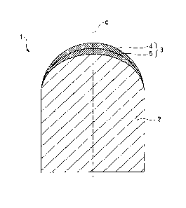
carbide; and a hard layer which is made of a sintered material of
polycrystalline
diamond harder than the tip body and is coated on a tip portion of the tip
body to
increase the tool life of a percussion drill bit is known. For example, PTL 1
proposes a
drilling tip which has a tip body which has a cylindrical posterior end
portion and a
hemispherical tip portion of which the outer diameter is reduced toward a tip
side; and
multiple hard layers, each formed of the polycrystalline diamond sintered
material,
which are coated on the tip portion of the tip body.
[0003]
In addition, as a drilling tip, a drilling tip which is joined to a tip of a
pick
CA 3021570 2023-05-25
CA 03021570 2018-10-18
2
attached to an outer periphery of a rotation drum of a drum drilling machine
for use in
opencast mining or longwall mining is known. PTL 2 proposes a drilling tip in
which a
substantially conical tip portion of a tip body is coated with diamond and/or
cubic boron
nitride. PTL 3 proposes that an outermost layer coated on a substantially
conical tip
portion of a tip body is selected from polycrystalline diamond,
polycrystalline cubic
boron nitride, single crystal diamond, and a cubic boron nitride composite
material.
[0004]
Regarding a cubic boron nitride sintered material, PTL 4 describes that a
high-hardness cubic boron nitride sintered material can be manufactured by
using a
metallic catalyst. In addition, PTL 5 proposes a cutting tool formed of a
cubic boron
nitride sintered material having a binder phase containing A120, A1B2, AIN,
TiB2, and
TiN in order to improve the strength and toughness.
Citation List
Patent Literature
[0005]
[PTL 1] United States Patent No. 4694918
[PTL 2] United States Patent No. 6051079
[PTL 3] European Patent Application, Publication No. 2053198
[PTL 4] Japanese Patent No. 5182582
[PTL 5] Japanese Unexamined Patent Application, First Publication No.
H8-197307
Summary of Disclosure
Technical Problem
CA 03021570 2018-10-18
3
[0006]
However, a polycrystalline diamond sintered material has lower toughness,
although having higher wear resistance than a cemented carbide. Accordingly, a
polycrystalline diamond sintered material has poor fracture resistance, and in
drilling of a
super-hard rock layer, a hard layer may chip or be damaged unexpectedly. In
addition, a
diamond sintered material cannot be used in Fe or Ni mines due to its high
affinity.
Moreover, its heat-resistant temperature is approximately 700 C, and thus the
diamond
sintered material cannot be used under conditions where it is exposed to a
temperature
higher than 700 C. For example, under high-temperature drilling condition of
700 C or
.. higher as in opencast mining which is performed under a dry environment,
diamond is
graphitized, and thus the wear resistance is reduced.
[0007]
In addition, a cubic boron nitride sintered material has a low affinity in Fe
or Ni
mines, but has a lower hardness than diamond. In the cubic boron nitride
sintered
material described in PTL 4, cracks are likely to occur due to a difference in
the
coefficient of thermal expansion between the binder phase of metal and the
cubic boron
nitride sintered material under high-temperature drilling conditions of 700 C
or higher as
above. Furthermore, the cubic boron nitride sintered material described in PTL
5 has a
relatively low hardness, and thus does not have sufficient wear resistance and
fracture
.. resistance, whereby it is difficult to use the cubic boron nitride sintered
material to a
drilling tool. In addition, in such a cubic boron nitride sintered material,
in a case where
the amount of cubic boron nitride grains contained in the sintered material is
increased to
improve the hardness, the cubic boron nitride grains are brought into contact
with each
other, and an unsintered portion which cannot sufficiently react with the
binder phase
.. increases. Therefore, there is a problem that a hardness corresponding to
the content of
CA 03021570 2018-10-18
4
the cubic boron nitride grains cannot be obtained.
[0008]
The disclosure is contrived based on such a background, and an object thereof
is
to provide a drilling tip which has a hardness comparable to a polycrystalline
diamond
sintered material, and can be used in Fe or Ni mines or under high-temperature
drilling
conditions, a drilling tool which has the drilling tip attached thereon, and a
method of
manufacturing the drilling tip.
Solution to Problem
[0009]
In order to achieve the object by solving the problems, a drilling tip
according to
the disclosure is a drilling tip which is attached to a tip portion of a
drilling tool to
perform drilling, the drilling tip including: a tip body which is provided
with a posterior
end portion buried in a tool body of the drilling tool, and a tip portion
protruding from a
surface of the drilling tool and being tapered toward a tip side of the tip
body; and a hard
layer which is formed on a surface of the tip portion of the tip body, in
which the hard
layer is provided with an outermost layer and an intermediate layer interposed
between
the outermost layer and the tip body, the outermost layer is a cubic boron
nitride sintered
material having 70 to 95 vol% of cubic boron nitride grains and a binder
phase, and when
a cross-sectional structure of the outermost layer is observed, a binder phase
having a
width of mm or greater and 30nm or less and containing Al, B, and N, and in
which a
ratio (atomic ratio) of an 0 content to an Al content is 0.1 or less exists
between
neighboring cubic boron nitride grains.
[0010]
In the drilling tip according to the disclosure, the outermost layer
preferably has
CA 03021570 2018-10-18
a Vickers hardness of 3,700 to 4,250. In addition, the cubic boron nitride
grains
preferably have an average grain size of 0.5 to 8.0 pm.
[0011]
When a cross-sectional structure of the outermost layer is observed, a ratio
of: a
5 number of cubic boron nitride grains which have the binder phase having a
width of lnm
or greater and 30nm or less, .and containing Al, B and N between neighboring
cubic
boron nitride grains: to a total number of the cubic boron nitride grains, is
0.4 or greater,
and a ratio of: a number of cubic boron nitride grains which have the binder
phase having
a width of mm or greater and 30nm or less, containing Al, B and N, and having
an
atomic ratio of an 0 content to an Al content of 0.1 or less between
neighboring cubic
boron nitride grains: to the number of cubic boron nitride grains which have
the binder
phase having a width of mm or greater and 30nm or less and containing Al, B
and N
between neighboring cubic boron nitride grains, is 0.5 or greater.
[0012]
The intermediate layer preferably contains 30 to 70 vol% of cubic boron
nitride
grains or diamond grains.
[0013]
A drill bit according to the disclosure includes a tool body; and the drilling
tip
which is attached to a tip portion of the tool body.
[0014]
A method of manufacturing a drilling tip according to the disclosure is a
method
of manufacturing a drilling tip having a tip body which is provided with a
posterior end
portion buried in a tool body of a drilling tool, and a tip portion protruding
from a surface
of the drilling tool and being tapered toward a tip side of the tip body, and
a hard layer
which is formed on a surface of the tip portion of the tip body, the hard
layer being
CA 03021570 2018-10-18
6
provided with an outermost layer and an intermediate layer interposed between
the
outermost layer and the tip body, the method including the steps of:
pretreating surfaces
of cubic boron nitride grains; obtaining a mixed powder by mixing a raw
material
powder for a binder phase of the outermost layer and the pretreated cubic
boron nitride
grains; and sintering the mixed powder, a raw material powder for the
intermediate layer,
and the tip body at a pressure of 5.0 GPa or greater and a temperature of
1,500 C or
higher.
Advantageous Effects of Disclosure
[0015]
A drilling tip according to the disclosure has a hardness comparable to a
polycrystalline diamond sintered material, and can be used in Fe or Ni mines
or under
high-temperature drilling conditions.
Brief Description of Drawings
[0016]
FIG. 1 is a cross-sectional view illustrating a drilling tip according to an
embodiment of the disclosure.
FIG 2 is a cross-sectional view illustrating a drill bit which has the
drilling tip
according to the embodiment illustrated in FIG 1 attached on a tip portion
thereof.
FIG 3 is a high angle annular dark field (HAADF) image (80,000
magnifications), taken by a scanning transmission electron microscope (STEM),
showing
an interface between two neighboring cubic boron nitride grains in a cross
section of an
outermost layer coated on a tip portion of the drilling tip.
FIG 4 is a binarized image of a mapping image of B in the visual field of FIG.
3.
CA 03021570 2018-10-18
vo,
7
FIG 5 is a binarized image of a mapping image of N in the visual field of FIG
3.
FIG. 6 is a binarized image of a mapping image of Al in the visual field of
FIG
3.
FIG 7 is a view illustrating a region in which B, N, and Al overlap each other
in
FIGS. 4 to 6.
FIG. 8 is a view illustrating a state in which the region (island) in which B,
N,
and Al overlap each other in FIG. 7 is approximated to an ellipse by an image
process.
FIG. 9 is a view in which an interface boundary line, formed of a polygonal
line
drawn by connecting midpoints of short axes of ellipses by straight lines, is
drawn in FIG.
8.
FIG 10 shows a view in which an interface boundary line is drawn in the region
in which B, N, and Al overlap each other in FIG. 7, and a partial enlarged
view
illustrating a width of a binder phase between cubic boron nitride grains
obtained from
the interface boundary line.
FIG. 11 is a view in which a measurement region having a width of 30 nm with
an interface boundary line as a center is drawn in FIG. 6.
FIG. 12 is a view in which a measurement region is drawn in a binarized image
of a mapping image of 0 in the visual field of FIG. 3.
FIG. 13 is a schematic view illustrating a method of measuring a ratio of the
number of cubic boron nitride grains with a binder phase, which has a width of
lnm or
greater and 30nm or less exists between neighboring cubic boron nitride
grains, to a total
number of cubic boron nitride grains.
FIG. 14 is a graph illustrating the relationship between the content of cubic
boron nitride grains and a Vickers hardness Hv.
CA 03021570 2018-10-18
=
8
Description of Embodiments
[0017]
FIG. 1 is a cross-sectional view illustrating a drilling tip according to an
embodiment of the disclosure. FIG 2 is a cross-sectional view illustrating a
drilling tool
according to an embodiment of the disclosure which has the drilling tip
according to the
embodiment attached thereon. The drilling tip according to this embodiment has
a tip
body 1, and this tip body 1 is provided with a body 2 which is made of a hard
material
such as a cemented carbide and a hard layer 3 which is coated on a surface of
at least a
tip portion (upper portion in FIG. 1) of the body 2 and has a higher hardness
(Vickers
hardness) than the body 2.
[0018]
In the tip body 1, a posterior end portion (lower portion in FIG. 1) has a
cylindrical or disk shape with a tip central line C as a center, and a tip
portion has a
hemispherical shape having a center on the tip central line C with the same
radius as that
of the cylindrical or disk shape of the posterior end portion in this
embodiment and is
formed into a tapered shape in which the outer diameter from the tip central
line C is
gradually reduced toward a tip side. That is, the drilling tip according to
this
embodiment is a button tip.
[0019]
In this embodiment, as illustrated in FIG. 1, only the tip portion of the tip
body 1
is coated with the hard layer 3, and the tip portion of the tip body 1
including the hard
layer 3 is formed to have the above-described hemispherical shape. In
addition, in this
embodiment, as illustrated in FIG. 1, the hard layer 3 has a two-layer
structure composed
of an outermost layer 4 and an intermediate layer 5 which is interposed
between the
outermost layer 4 and the body 2.
CA 03021570 2018-10-18
9
[0020]
A drill bit as an embodiment of the drilling tool which has the drilling tip
attached on the tip portion thereof has a bit body 11 made of steel or the
like and has a
substantially bottomed cylindrical shape with an axial line 0 as a center as
illustrated in
FIG. 2. The bottomed portion of the bit body is a tip portion (upper portion
in FIG. 2),
and the drilling tip is attached on the tip portion. In addition, a female
thread portion 12
is formed at the inner periphery of a posterior end portion (lower portion in
FIG 2) of the
cylindrical shape, and a drill rod (not shown) connected to a drilling machine
is screwed
in the female thread portion 12. By transmission of a striking force and an
impelling
force toward a tip side in a direction of the axial line 0 and a rotating
force around the
axial line 0 from the drill rod to the female thread portion 12, the drilling
tip breaks
bedrock, thereby forming a borehole.
[0021]
The tip portion of the bit body 11 has a slightly larger outer diameter than
the
posterior end portion. At the outer periphery of the tip portion, a plurality
of discharge
grooves 13 extending in parallel to the axial line 0 are formed at intervals
in a
circumferential direction. Crushed rubbish generated by breaking bedrock using
the
drilling tip is discharged to a posterior end side of the bit body 11 through
the discharge
grooves 13. In addition, a blow hole 14 is formed along the axial line 0 from
a bottom
surface of the female thread portion 12 of the bottomed bit body 11. This blow
hole 14
is obliquely branched in the tip portion of the bit body 11 and opened to a
tip surface of
the bit body 11. A fluid such as compressed air supplied via the drill rod is
ejected from
the blow hole 14, and thus discharge of crushed rubbish is promoted.
[0022]
The tip surface of the bit body 11 is provided with a circular face surface 15
CA 03021570 2018-10-18
=
around an axial line 0 perpendicular to the axial line 0 on the inner
peripheral side as a
center and a frustconical gauge face 16 positioned at an outer periphery of
the face
surface 15 and extending toward the posterior end side as extending toward the
outer
periphery side. The blow hole 14 is opened to the face surface 15, and a tip
of the
5 discharge groove 13 is opened to the outer peripheral side of the
frustconical gauge face
16. Each of the face surface 15 and the frustconical gauge face 16 has a
plurality of
fitting holes 17 having a circular cross section that are formed perpendicular
to the face
surface 15 and the frustconical gauge face 16 to avoid the opening portions of
the blow
hole 14 and the discharge groove 13.
10 [0023]
The drilling tip is attached in such a manner that it is fitted in by
pressing, shrink
fitting, or the like, or brazed to be fixed to, that is, buried in the fitting
holes 17, in a state
in which the posterior end portion of the tip body 1 is buried as illustrated
in FIG. 2.
The tip portion of the tip body 1 having the hard layer 3 formed thereon
protrudes from
the face surface 15 and the frustconical gauge face 16 and breaks bedrock with
the
above-described striking force, impelling force, and rotating force.
[0024]
Next, a configuration of the outermost layer 4 of the hard layer 3 will be
described using FIGS. 3 to 13. The outermost layer 4 is formed of a cubic
boron nitride
sintered material (hereinafter, also referred to as "cBN sintered material")
in which the
main binder phase is formed of ceramics. The cBN sintered material includes
cubic
boron nitride grains (hereinafter, also referred to as "cBN grains") of which
the content is
70 to 95 vol% with respect to the whole cBN sintered material, and a binder
phase
binding the cBN grains to each other. In a cross-sectional structure seen by
observing
an optional cross section of the outermost layer 4, a binder phase having a
width of lrun
CA 03021570 2018-10-18
11
or greater and 30nm or less exists between neighboring cBN grains. This binder
phase
includes at least aluminum (Al), boron (B), and nitrogen (N), and a ratio
(0/A1) of the
oxygen (0) content to the Al content in the binder phase is 0.1 or less
(atomic ratio
calculated from an area ratio of the cross section). The lower limit value of
the ratio of
the 0 content to the Al content is 0.
[0025]
The above-described binder phase strongly binds the cBN grains to each other
since it has a low oxide content. In addition, in the cBN sintered material
having the
above-described binder phase, the cBN grains are brought into contact with
each other,
and an unsintered portion which cannot sufficiently react with the binder
phase is small.
Therefore, such a cBN sintered material has a high hardness. By forming the
outermost
layer 4 using such a cBN sintered material, the drilling tip can have a
hardness
comparable to a polycrystalline diamond sintered material, and thus the wear
resistance
of the drilling tip can be secured. In a case where no binder phase, having a
width of
mm or greater and 30nrn or less and containing Al, B, and N, and in which a
ratio
(atomic ratio) of the 0 content to the Al content is 0.1 or less, exists
between neighboring
cBN grains, the cBN grains cannot be sufficiently bound, and thus the
outermost layer 4
has a low hardness, or breakage starting from the inside of the binder phase
is likely to
Occur.
[0026]
As long as the main binder phase is formed of ceramics, the configuration of a
binder phase other than the binder phase having a width of mm or greater and
30nm or
less and existing between neighboring cBN grains among the binder phases
formed in the
cBN sintered material is not particularly limited, and preferably includes one
or more
selected from a nitride, a carbide, a carbonitride, and a boride of Ti, a
nitride, a boride,
CA 03021570 2018-10-18
=
12
and an oxide of Al, and solid solutions of two or more thereof; and inevitable
impurities.
[0027]
The Vickers hardness of the outermost layer 4 is preferably 3,700 to 4,250. In
a case where the Vickers hardness is less than 3,700, it is difficult to
impart sufficient
wear resistance to the outermost layer 4. In a case where the Vickers hardness
is greater
than 4,250, the outermost layer 4 is likely to fracture.
[0028]
Since the content of the cBN grains in the outermost layer 4 is 70 to 95 vol%,
the above-described cross-sectional structure can be formed, and the Vickers
hardness of
the outermost layer 4 can be adjusted within the above-described range. In a
case where
the content of the cBN grains is less than 70 vol%, the amount of the cBN
grains is small,
and thus the Vickers hardness of the outermost layer 4 cannot be adjusted to
3,700 or
greater. In addition, it is difficult to form a binder phase having a width of
mm or
greater and 30tun or less between the cBN grains. Furthermore, between the cBN
grains, the amount of a compound containing Al, B, and N in the binder phase
becomes
relatively smaller than that of a binder phase component (for example, Ti or
Ta
compound or boride of Al) other than the above compound. Therefore, uniform
sintering cannot be performed, and a structure exhibiting the above-described
effects
cannot be obtained. That is, in comparison to the binder phase containing Al,
B, and N,
the Ti compound or Al boride has a low adhesion strength to the cBN grains,
and thus an
interface between the Ti compound or Al boride and the cBN grains is likely to
become a
starting point of cracks. As a result, the fracture resistance is reduced. In
a case where
the content of the cBN grains is greater than 95 vol%, voids to be a starting
point of
cracks are likely to be formed in the sintered material, and thus the fracture
resistance is
reduced. The content of the cBN grains is preferably 70 to 92 vol%, and more
CA 03021570 2018-10-18
13
preferably 75 to 90 vol%, but not limited thereto.
[0029]
The average grain size of the cBN grains is preferably 0.5 to 8.0 p.m. In a
case
where such cBN grains are dispersed in the cBN sintered material, high
fracture
resistance can be imparted to the outermost layer 4. Specifically, it is
possible to
suppress the occurrence of chipping starting from irregularities formed due to
falling-off
of the cBN grains from a surface of the outermost layer 4 during drilling. In
addition,
propagation of cracks proceeding from the interface between the cBN grains and
the
binder phase or cracks proceeding through the cBN grains, occurring by a
stress applied
to the outermost layer 4 during drilling, can be suppressed by the cBN grains
dispersed in
the cBN sintered material. The average grain size of the cBN grains is more
preferably
0.5 to 3.0 p.m, but not limited thereto.
[0030]
In a case where a visual field in which one side is 5 times the average grain
size
of the cBN grains is set as one visual field, it is preferable that in the
observation of an
optional cross section of the outermost layer 4 in 5 or more visual fields,
between
neighboring cBN grains, a binder phase having a width of lnrn or greater and
30nm or
less and containing Al, B, and N, and in which a ratio 0/A1 of the 0 content
to the Al
content is 0.1 or less, be observed in 60% or greater of the total number of
visual fields
observed. The fact that the content of such a binder phase is large means that
there are
many networks in which the neighboring cBN grains are strongly bound by the
binder
phase. Accordingly, the larger the number of visual fields in which such a
binder phase
is observed, the more excellent the hardness of the outermost layer 4. The
number of
visual fields in which such a binder phase is observed is more preferably 80%
or greater
of the total number of visual fields, and even more preferably 100% (the
binder phase is
CA 03021570 2018-10-18
14
observed in all of the visual fields).
[0031]
In the observation of an optional cross section of the outermost layer 4, a
ratio
(q/Q) of the number (q) of cBN grains with a binder phase, which has a width
of lnm or
greater and 30nm or less and includes Al, B and N between the neighboring cBN
grains,
to the number (Q) of all of the cBN grains is preferably 0.4 or greater. In
addition, a
ratio (n/N) of the number (n) of cBN grains with a binder phase, which has a
width of
Inan or greater and 30nm or less, includes Al, B and N, and exists between the
neighboring cBN grains, and in which a ratio 0/A1 of the 0 content to the Al
content is
0.1 or less, to the number (N) of cBN grains with a binder phase, which has a
width of
mm or greater and 30nm or less, includes Al, B and N, and exists between the
neighboring cBN grains, is preferably 0.5 or greater. The fact that the ratio
q/Q and the
ratio n/N are high means that the cBN grains are strongly bound by the binder
phase.
Accordingly, in a case where the ratio q/Q is 0.4 or greater and the ratio n/N
is 0.5 or
greater, the hardness of the outermost layer 4 can be improved. The upper
limit of the
value of the ratio q/Q is preferably 1, and the value of q/Q is more
preferably 0.6 to 1.
The value of the ratio n/N is preferably 0.6 to 1, and more preferably 0.8 to
1.
[0032]
The binder phase which exists between neighboring cBN grains, has a width of
mm or greater and 30nm or less, and contains Al, B, and N may exist in places
between
the neighboring cBN grains, or one binder phase may extend between the cBN
grains (a
cBN grain may be adjacent to another cBN grain via one binder phase described
above).
[0033]
Regarding the outermost layer 4 of the drilling tip according to this
embodiment,
procedures for specifying the above-described configuration will be described
CA 03021570 2018-10-18
hereinafter.
[0034]
<Average Grain Size of cBN Grains>
The average grain size of the cBN grains can be obtained as follows.
5 First, a cross-sectional structure of the cBN sintered material is
observed by a
scanning electron microscope (SEM) to obtain a secondary electron image. For
example, in a case where the average grain size of the cBN grains before
sintering is 3
pm, the secondary electron image has a size of 15 x 15 p.m (5-time angle of
the
average grain size of the cBN grains before sintering).
10 [0035]
Next, the secondary electron image is displayed in monochrome with 256 shades
of gray ranging from 0 corresponding to black to 255 corresponding to white.
Using an
image having such a pixel value that the ratio of a pixel value of cBN grain
portions to a
pixel value of binder phase portions is 2 or greater, a binarization process
is performed
15 such that the cBN grains are black. In this image, the pixel value of
the cBN grains
portions or the binder phase portions is obtained from an average within a
region of
approximately 0.5 IM1 X 0.5 tn. It is preferable that in the same image,
average pixel
values of at least 3 regions be obtained, and the obtained values be defined
as contrast of
the regions. Accordingly, the cBN grains and the binder phase are
distinguished from
each other. After the above-described binarization process, a separation
process is
performed for a portion thought to be cBN grains brought into contact with
each other.
For example, cBN grains thought to be brought into contact with each other are
separated
using watershed as an image process operation. In this manner, portions
corresponding
to cBN grains are extracted by the image process from the image obtained by
performing
the binarization process on the secondary electron image.
CA 03021570 2018-10-18
16
[0036]
The portions (black portions) corresponding to the cBN grains extracted by the
above-described process are subjected to grain analysis, and maximum lengths
of the
portions corresponding to the cBN grains are obtained, respectively. The
obtained
maximum lengths are defined as maximum lengths of the respective cBN grains,
and the
maximum lengths are defined as diameters of the respective cBN grains. Volumes
of
the respective cBN grains are calculated from the obtained diameters by
assuming that
the cBN grains are spheres. Based on the volumes of the respective cBN grains,
a
cumulative distribution of the grain sizes of the cBN grains is obtained.
Specifically,
the sum of the volumes of the respective cBN grains and the volumes of cBN
grains
having a diameter which is not greater than the diameters of the above cBN
grains is
obtained as an integrated value. Regarding the respective cBN grains, a graph
having a
vertical axis representing a volume percentage [%] which is a ratio of the
integrated
value of the respective cBN grains to the sum of the volumes of all of the cBN
grains and
a horizontal axis representing a diameter [i.tm] of the respective cBN grains
is drawn. A
diameter (median diameter) in which the volume percentage is 50 vol% is
defined as an
average grain size of the cBN grains in one image.
[0037]
The average of the average grain sizes obtained by performing the
above-described process on at least 3 secondary electron images is defined as
an average
grain size [1.1.m] of the cBN grains in the outermost layer 4. In such grain
analysis, a
length (p.m) per pixel is set using a value of a scale known in advance by
SEM. In
addition, in the grain analysis, a region having a diameter which is less than
0.02 pm is
not calculated as a grain in order to remove noise.
CA 03021570 2018-10-18
17
[0038]
<Content of cBN Grains>
The content of the cBN grains can be adjusted by adjusting the mixing ratio
between a cBN grain powder and a raw material powder for binder phase
formation in
the formation of the outermost layer 4. The content can be confirmed as
follows. That
is, an optional cross section of the outermost layer 4 is observed by SEM to
obtain a
secondary electron image. In the obtained secondary electron image, portions
corresponding to cBN grains are extracted by the same image process as above.
An
area occupied by the cBN grains is calculated by image analysis, and a ratio
of the cBN
grains in one image is obtained. The average of the contents of the cBN grains
obtained
by processing at least 3 images is defined as a content of the cBN grains in
the outermost
layer 4. A square region in which one side has a length which is 5 times the
average
grain size of the cBN grains is preferably an observation region used in the
image process.
For example, in a case where the cBN grains have an average grain size of 3
m, a visual
field region of approximately 15 tm x 15 vim is preferable.
[0039]
<Binder Phase Which Exists Between Neighboring cBN Grains, Having Width
of mmn or greater and 30nm or less, and Containing Al, B, and N>
Whether a binder phase having a width of mm or greater and 30run or less and
containing Al, B, and N exists between neighboring cBN grains is observed as
follows.
First, an optional cross section of the outermost layer 4 is polished, and an
interface
between two neighboring cBN grains illustrated in FIG. 3 is observed using a
scanning
transmission electron microscope (STEM). FIG 3 is a high angle annular dark
field
(HAADF) image (80,000 magnifications), taken by observing the interface
between the
cBN grains using the STEM. The thickness of the observation sample is
preferably 3
CA 03021570 2018-10-18
18
nm to 70 nm. It is not preferable that the thickness be smaller than 3 nm
since the
quantity of characteristic X-rays to be detected is reduced in elemental
mapping, and thus
a long period of time is taken for the measurement, and the sample is likely
to be
damaged. It is not preferable that the thickness be larger than 70 nm, since
it becomes
difficult to perform image analysis. The size of the observation image is
increased from
150 nm (vertical) x 150 nm (horizontal) to approximately 500 nm (vertical) x
500 nm
(horizontal), and the resolution is increased to 512 x 512 pixels or more.
[0040]
Next, in the same observation region, elemental mapping images (see FIGS. 4 to
6 and 12) of B, N, Al, and 0 are obtained. These elemental mapping images are
images
obtained by conversion into a ratio (atm%) of the content of each element with
respect to
a total of the contents of the four elements in order to remove the
background. Based
on these images, whether a binder phase having a width of mm or greater and
30nm or
less and containing Al, B, and N exists between neighboring cBN grains is
confirmed in
accordance with the following procedures (a) to (d), and a ratio of Al and a
ratio of 0 in
the binder phase is obtained.
[0041]
(a) From the mapping images of B and N (see FIGS. 4 and 5), it is confirmed
that the observed region is a region in which two or more cBN grains exist and
an
observation target region.
(b) The mapping image of Al (FIG. 6), the mapping image of B (FIG. 4), and the
mapping image of N (FIG. 5) are superimposed to specify a region in which
these
mapping images overlap each other as a binder phase existing between cBN
grains and
containing Al, B, and N (FIG 7). The width of the binder phase is determined
as
follows.
CA 03021570 2018-10-18
19
(bl) In a case where one binder phase extends between cBN grains, that is, in
a
case where one Al island overlaps with a region in which B and N exist, first,
a long axis
is obtained in the mapping image of Al when the Al island corresponding to the
binder
phase is approximated to an ellipse. Specifically, the Al island overlapping
the region in
which B and N exist is extracted by an image process in the same manner as in
the
above-described measurement of the average grain size of the cBN grains, and a
maximum length is defined as a long axis when the extracted island is
approximated to
an ellipse by image analysis. This long axis is defined as an interface
boundary line
between the cBN grains.
(b2) In a case where a binder phase exists in places between cBN grains, that
is,
in a case where an Al island overlapping a region in which B and N exist is
divided into
two or more, the Al islands overlapping the region in which B and N exist are
extracted
by an image process in the same manner as in the above-described measurement
of the
average grain size of the cBN grains (FIG. 7). Next, each of the islands
extracted by the
image process is approximated to an ellipse (FIG 8). In addition, a short axis
of each
ellipse is obtained. In each short axis, a midpoint is obtained, and
neighboring
midpoints are connected by straight lines to draw a polygonal line T. This
polygonal
line T is defined as an interface boundary line between the cBN grains (FIGS.
9 and 10).
(b3) In the mapping image of Al, a width of the Al island overlapping the
interface boundary line obtained in (b 1) or (b2) in a direction perpendicular
to the
interface boundary line is measured (FIG. 10). The width of the Al island is
measured at
at least 3 places. Specifically, in a case where 3 or more Al islands exist,
maximum
widths of at least 3 Al islands are measured. The average of the measured
widths is
defined as a width of a binder phase existing between neighboring cBN grains.
In a
case where the number of Al islands is 2 or smaller, maximum widths of the Al
islands
CA 03021570 2018-10-18
= =
are measured. In a case where the width is lnm or greater and 30nm or less,
the width
of the binder phase existing between the cBN grains and containing Al, B, and
N is
regarded to be mm or greater and 30nm or less.
[0042]
5 (c) Next, the Al content and the 0 content of the binder phase are
obtained as
follows. First, using images (FIGS. 11 and 12) obtained by subjecting the
mapping
images of Al and 0 to a binarization process, a measurement region M having a
width of
nm with the interface boundary line confirmed in (b) as a center is
determined. This
region M is a region surrounded by two congruent lines, which are parallel to
and
10 separated from the interface boundary line by a distance of 15 nm, and
two straight lines
connecting end portions of the region M. From the image obtained by subjecting
the
mapping image of Al to the binarization process, an area of Al of a portion
where B, N,
and Al overlap in the region M is obtained. Similarly, an area of 0 in the
region M is
obtained. A ratio (area%) of the area of 0 to the area of Al obtained as above
in the
15 .. region M is defined as a ratio 0/A1 (atomic ratio) of the 0 content to
the Al content in the
binder phase.
[0043]
<Ratio (q/Q) of cBN Grains in which Binder Phase Having Width of mm or
greater and 30nm or less and Containing Al, B, and N Exists Between
Neighboring cBN
20 Grains>
The ratio (q/Q) of the number (q) of cBN grains with a binder phase, which has
a width of mm or greater and 30nm or less and includes Al, B and N, between
neighboring cBN grains, to the number (Q) of all of the cBN grains can be
measured as
follows. First, in an optional cross section of the outermost layer 4, a
square region in
25 which a length L of one side is 5 times the average grain size of cBN
grains 10 is
CA 03021570 2018-10-18
21
determined as one measurement visual field range A as illustrated in the
schematic view
of FIG. 13. For example, in a case where the average grain size of the cBN
grains is 1
lam, a square region of 5 liM X 5 tm is determined as one measurement visual
field
range.
[0044]
Next, a diagonal line D is drawn from a vertex of the square measurement
visual
field range A, and the number Qi of cBN grains 10 overlapping the diagonal
line D is
counted. In addition, whether a binder phase 20 having a width of lnm or
greater and
30nm or less and containing Al, B, and N exists between each of the cBN grains
10
overlapping the diagonal line D and a cBN grain 10 neighboring thereto is
specified by
the above-described method. The number qi of cBN grains 10 specified as being
grains
with a binder phase 20, which has a width of mm or greater and 30nm or less
and
includes Al, B and N between the neighboring cBN grains, 10 is counted. Using
the
number qi of cBN grains 10 and the number Qi of cBN grains 10 obtained, a
value of
qi/Qi is calculated. qi/Q1 is calculated in at least 5 visual fields, and an
average thereof
is defined as the above-described ratio q/Q.
[0045]
<Ratio (n/N) of cBN Grains in Which Binder Phase Having Width of mm or
greater and 30nm or less and Containing Al, B, and N, and in Which Ratio of 0
Content
to Al Content is 0.1 or less Exists Between Neighboring cBN Grains>
The ratio (n/N) of the number (n) of cBN grains with a binder phase, which has
a width of mm or greater and 30nm or less and includes Al, B, and N, and in
which a
ratio 0/A of the 0 content to the Al content is 0.1 or less exists between the
neighboring
cBN grains, to the number (N) of cBN grains with a binder phase, which has a
width of
lnm or greater and 30nm or less and includes Al, B and N between the
neighboring cBN
CA 03021570 2018-10-18
22
grains, can be measured as follows. First, in the schematic view of FIG. 13,
as
described above, cBN grains 10 with a binder phase 20, which has a width of
lnm or
greater and 30nm or less and includes Al, B and N between the cBN grains, 10
are
specified among the cBN grains overlapping the diagonal line D, and the number
N1 of
the above cBN grains is counted. Next, among these cBN grains 10, cBN grains
10 in
which the ratio 0/A1 of the 0 content to the Al content of a binder phase 20
having a
width of 1= or greater and 30nm or less and containing Al, B, and N is 0.1 or
less are
specified by the above-described method, and the number n1 of the above cBN
grains is
counted. Using the number ni of cBN grains 10 and the number N1 of cBN grains
10
obtained, a value of ni/Ni is calculated. n1/N1 is calculated in at least 5
visual fields,
and an average thereof is defined as the above-described ratio n/N.
[0046]
At least one intermediate layer 5 is provided between the outermost layer 4
and
the body 2. Accordingly, it is possible to prevent the outermost layer 4 from
being
peeled. That is, in a case where an outermost layer 4 formed of the above-
described
cBN sintered material is directly formed on the body 2, a stress remains after
sintering
due to a difference in the shrinkage ratio between the outermost layer 4 and
the body 2
made of a hard material such as a cemented carbide, and cracks occur between
an
interface between the body 2 and the outermost layer 4. In this embodiment,
since the
intermediate layer 5 is provided between the outermost layer 4 and the body 2,
the
intermediate layer 5 functions as a stress relaxation layer. As a result, it
is possible to
suppress the occurrence of cracks, and it is possible to prevent the outermost
layer 4 from
being peeled.
[0047]
The configuration of the intermediate layer 5 is not particularly limited as
long
CA 03021570 2018-10-18
23
as the intermediate layer has a less hardness (Vickers hardness) which is less
than the
outermost layer 4 and greater than the body 2. For example, the intermediate
layer 5
may be a cBN sintered material obtained by sintering with a catalytic metal
containing Al
and at least one of Co, Ni, Mn, and Fe. In addition, a metallic additive
containing at
least one of W, Mo, Cr, V, Zr, and Hf may be added to the metallic catalyst.
The
intermediate layer 5 may be formed of a polycrystalline diamond sintered
material
including diamond, cobalt, and tungsten carbide.
[0048]
Here, the intermediate layer 5 preferably contains 30 to 70 vol% of cBN grains
or diamond grains. In a case where the content of the cBN grains or diamond
grains
which are hard grains is 30 vol% or less, the intermediate layer 5 has a less
hardness than
the body 2. In a case where the content is 70 vol% or greater, the
intermediate layer 5
has the same hardness as the outermost layer 4. Accordingly, the content of
the cBN
grains or diamond grains in the intermediate layer 5 is preferably 30 to 70
vol% to allow
the intermediate layer to function as a stress relaxation layer.
[0049]
In this embodiment, the intermediate layer 5 has a single layer structure.
However, the intermediate layer 5 may have a multi-layer structure. In a case
where the
intermediate layer 5 has a multi-layer structure of 3 layers or more, it is
preferable that
from the side of the outermost layer 4 toward the side of the body 2, the
content of the
cBN grains or diamond grains in the intermediate layer 5 be reduced and the
Vickers
hardness be thus reduced.
[0050]
The thickness of the outermost layer 4 on the tip central line C is preferably
0.3
mm to 1.5 mm. In a case where the thickness of the outermost layer 4 is 0.3 mm
or
CA 03021570 2018-10-18
24
smaller, there is a concern that the drilling tip may be rapidly abraded and
its life may
thus be reduced. In a case where the thickness of the outermost layer 4 is 1.5
mm or
larger, there is a concern that cracks may be likely to occur due to a
residual stress during
sintering, and thus unexpected fractures may be caused during drilling. The
thickness
of the outermost layer 4 is more preferably 0.4 mm to 1.3 mm. In addition, the
total
thickness of the intermediate layer 5 on the tip central line C is preferably
0.2 mm to 1.0
mm. In
a case where the thickness of the intermediate layer 5 is 0.2 mm or smaller,
there is a concern that it may be difficult to form a uniform layer, and thus
it may be
difficult to absorb a residual stress during sintering, and the intermediate
layer may not
function to relax the stress of the tip. In a case where the thickness of the
intermediate
layer 5 is 1.0 mm or larger, the total thickness of the hard layer 3
(outermost layer 4 and
intermediate layer 5) is increased, and thus there is a concern that cracks
may be likely to
occur due to a residual stress during sintering, and thus unexpected fractures
may be
caused during drilling. The total thickness of the intermediate layer 5 is
more
preferably 0.3 mm to 0.8 mm.
[0051]
Next, a method of manufacturing a drilling tip including the outermost layer 4
and the intermediate layer 5 described above will be described.
The method of manufacturing a drilling tip according to this embodiment
includes a step of performing a pretreatment on surfaces of cBN grains, a step
of
obtaining a mixed powder of the pretreated cBN grains and a raw material
powder for a
binder phase of the outermost layer 4, and a step of sintering the mixed
powder, a raw
material powder for the intermediate layer 5, and the body 2.
[0052]
The pretreatment for surfaces of cBN grains is performed as follows to obtain
CA 03021570 2018-10-18
cBN grains having a high surface cleanliness. First, an AIN film having a very
small
film thickness is formed on surfaces of cBN grains. As a film forming method,
for
example, an atomic layer deposition (ALD) method can be used. The ALD method
is a
type of CVD method, and is a method of reacting a base material in a vacuum
chamber
5 with molecules of a raw material compound for each layer to repeatedly
perform purge
by Ar or nitrogen, thereby forming a film. Specifically, first, cBN grains as
a base
material are charged into a fluidized bed furnace, and the temperature in the
furnace is
increased to approximately 350 C. Next, a cycle of an Ar+Al(CH3)3 gas inflow
step, an
Ar gas purge step, an Ar-FNH3 gas inflow step, and an Ar gas purge step is
repeatedly
10 performed until a desired AIN film thickness is obtained. For example,
an AIN film
having a film thickness of approximately 5 nm can be coated on the surfaces of
the cBN
grains by film formation for 30 minutes.
[0053]
Next, the cBN grains coated with the AIN film are heated at approximately
15 1,000 C under vacuum. Accordingly, impurity elements such as oxygen of
the surfaces
of the cBN grains are diffused and captured in the AIN film. Finally, by
mixing the
cBN grains through ball-mill mixing, the AIN film capturing the impurity
elements is
peeled from the surfaces of the cBN grains.
[0054]
20 By performing such a pretreatment on the cBN grains, cBN grains having
a high
surface cleanliness, in which impurity components such as oxygen are removed
from
surfaces, are obtained. The pretreatment for surfaces of cBN grains is not
limited to the
above-described treatment, and any method can be used as long as it is a
method for
removing impurity components of the surfaces of the cBN grains.
25 [0055]
CA 03021570 2018-10-18
26
Next, the pretreated cBN grains are mixed with a raw material powder for a
binder phase of the outermost layer 4 to obtain a predetermined composition,
and a
mixed powder is obtained. As the raw material powder for a binder phase of the
outermost layer 4, a TiN powder, an Al powder, a TiA13 powder, and an A1203
powder
can be used.
[0056]
Then, the obtained mixed powder, a raw material powder for the intermediate
layer 5, and the body 2 are subjected to ultra-high-pressure and high-
temperature
sintering. In this manner, by integrally sintering the outermost layer 4, the
intermediate
layer 5, and the body 2, the tip body 1 of the drilling tip according to this
embodiment
can be manufactured.
[0057]
According to the manufacturing method of this embodiment, the outermost layer
4 having the above-described configuration can be formed by using, as cBN
grains of the
outermost layer 4, cBN grains of which the surface cleanliness has been
increased by the
pretreatment, and by subjecting the cBN grains to ultra-high-pressure and
high-temperature sintering. In addition, the sintering is preferably performed
at a
temperature of 1,500 C or higher with a pressure of 5.0 GPa or greater in a
stable region
of diamond and cubic boron nitride. Accordingly, the outermost layer 4 and the
.. intermediate layer 5 can be simultaneously formed on the body 2. The
sintering
pressure is more preferably 5.5 GPa to 8.0 GPa, and the sintering temperature
is more
preferably 1,600 C to 1,800 C. The above step is preferably performed to
prevent
oxidation of the raw material powder, and specifically, the raw material
powder or
molded body is preferably handled under a non-oxidizing protective atmosphere.
[0058]
CA 03021570 2018-10-18
A
27
The drilling tip, the drilling tool, and the method of manufacturing a
drilling tip
according to the embodiment of the disclosure have been described, but the
disclosure is
not limited thereto, and can be appropriately changed without departing from
the
technical ideas of the disclosure. In this embodiment, a case where the
disclosure is
applied to a button-type drilling tip in which the tip portion of the tip body
1 has a
hemispherical shape has been described as above. However, the disclosure can
also be
applied to a so-called ballistic-type drilling tip in which a tip portion of a
tip body 1 has a
shell shape, or a so-called spike-type drilling tip in which a tip portion on
a posterior end
side has a conical surface shape of which the diameter is reduced toward a tip
side, and a
tip thereof has a spherical shape with a radius smaller than that of a
cylindrical posterior
end portion of a tip body 1.
[0059]
In addition, in this embodiment, a case where the drilling tip is applied to a
drill
bite has been described, but the drilling tip according to the disclosure can
also be
applied to a pick attached to an outer periphery of a rotation drum of a drum
drilling
machine for use in opencast mining or longwall mining.
Examples
[0060]
Next, the effects of the disclosure will be shown using examples of a drilling
tip
and a drill bit according to the disclosure.
[0061]
(First Example)
First, with examples of a cBN sintered material constituting an outermost
layer
as First Example, the effects of the disclosure will be shown.
CA 03021570 2018-10-18
28
[0062]
cBN grains having a median diameter (D50) shown in Table 1 were used as a
base material, and through an ALD method, an AIN film having an average film
thickness shown in Table 1 was coated thereon. Specifically, first, cBN grains
were
charged into a furnace, and the temperature in the furnace was increased to
350 C.
Next, using a film forming gas which was an Al(CH3)3 gas as an Al precursor
and a
reaction gas which was a NH3 gas, a cycle of the following (1) to (4) was
repeated until
an AIN film having a target film thickness was formed.
(1) Ar+Al(CH3)3 gas inflow step
(2) Ar gas purge step
(3) Ar+NH3 gas inflow step
(4) Ar gas purge step
The cBN grains were observed by SEM, and thus an AIN film having an average
film thickness shown in Table 1 was confirmed to be coated on surfaces of the
cBN
grains.
[0063]
Next, the cBN grains coated with the AIN film were heat-treated for 30 minutes
at approximately 1,000 C under vacuum to diffuse impurity elements such as
oxygen of
the surfaces of the cBN grains in the AIN film. The heat-treated cBN grains
were mixed
through ball-mill mixing using a tungsten carbide container and balls, and the
AIN film
was peeled from the surfaces of the cBN grains.
[0064]
A TiN powder, a TiC powder, an Al powder, a TiA13 powder, and a WC powder
having an average grain size within a range of 0.3 to 0.9 i.tm were prepared
as raw
material powders for a binder phase. Two or more selected from the above raw
material
CA 03021570 2018-10-18
29
powders and the cBN grain powder pretreated as described above were blended
such that
the content of the cBN grain powder was 70 to 95 vol% in a case where the
total amount
of the powders was 100 vol%. Then, the mixture was subjected to wet blending
and
dried. Thereafter, the mixture was press-molded into dimensions of 50 mm in
diameter
and 1.5 mm in thickness at a molding pressure of 1 MPa using a hydraulic press
to obtain
a molded body. Next, the molded body was heat-treated by being held for 30 to
60
minutes at a predetermined temperature within a range of 1,000 C to 1,300 C
under a
vacuum atmosphere at 1 Pa, and was then charged into an ultra-high-pressure
sintering
apparatus and subjected to ultra-high-pressure and high-temperature sintering
for 30
minutes at 5.0 GPa and 1,600 C. Thus, cBN sintered materials 1 to 17 of a
drilling tip
of the present disclosure (hereinafter referred to as "cBN sintered materials
1 to 17 of the
present disclosure") shown in Table 2 were prepared.
[0065]
For comparison, comparative cBN sintered materials 1 to 10 were prepared as
follows. First, cBN grains a to i having a median diameter (D50) shown in
Table 4 were
prepared. The cBN grains a, b, and e to i were not pretreated in the same
manner as in
the cases of the cBN sintered materials 1 to 17 of the present disclosure. The
cBN
grains c and d were pretreated in the same manner as in the cases of the cBN
sintered
materials 1 to 17 of the present disclosure, so that an AIN film having an
average film
thickness shown in Table 4 was formed on surfaces of the cBN grains, and then
peeled
therefrom.
[0066]
Two or more selected from the same raw material powders for a binder phase as
in the cases of the above-described cBN sintered materials 1 to 17 of the
present
disclosure and the cBN grain powder were blended such that the content of the
cBN grain
CA 03021570 2018-10-18
powder was 55 to 98.2 vol% in a case where the total amount of the powders was
100
vol%. Next, the comparative cBN sintered materials 1 to 10 shown in Table 5
were
manufactured in accordance with the same procedures as in the cases of the
above-described cBN sintered materials 1 to 17 of the present disclosure.
5 [0067]
Regarding the cBN sintered materials 1 to 17 of the present disclosure and the
comparative cBN sintered materials 1 to 10, a binder phase structure other
than cBN was
confirmed by X-ray diffraction (XRD). In addition, regarding the cBN sintered
materials 1 to 17 of the present disclosure and the comparative cBN sintered
materials 1
10 to 10, the average grain size (am) of the cBN grains and the content
(vol%) of the cBN
grains were measured by the above-described methods, respectively. The
observation
region used in the image process had a size of 15 pm x 15 p.m. The results are
shown in
Tables 2 and 5.
[0068]
15 At 10 points on a polished surface of each of the cBN sintered
materials 1 to 17
of the present disclosure and the comparative cBN sintered materials 1 to 10,
a Vickers
hardness (Hv) was measured at a load of 5 kg. The average of the measured
values is
shown in Tables 2 and 5 as an average Vickers hardness. Each value was rounded
off to
the nearest 10. In addition, a graph obtained by plotting the relationship
between the
20 cBN content C (vol%) and the Vickers hardness H (Hv) of Tables 2 and 5
is shown in
FIG. 14.
[0069]
The presence or absence of a binder phase having a width of lnm or greater and
30nm or less between neighboring cBN grains, and the presence or absence of
Al, B, and
25 N in the binder phase were confirmed by the above-described methods,
respectively, and
CA 03021570 2018-10-18
31
a ratio 0/A1 of the 0 content to the Al content in the binder phase was
calculated by the
above-described method. The ratio 0/A1 was measured at 5 places, and the
average
thereof was calculated. The results are shown in Tables 2, 3, 5, and 6. In the
tables,
"-" means that although a binder phase having a width of mm or greater and
30nm or
less exists between neighboring cBN grains, there are no overlapping portions
of Al, B,
and N elements, and thus the interface boundary line could not be defined, and
the ratio
0/A1 could not be calculated.
[0070]
In addition, the presence or absence of a binder phase which had a width of
lnm
or greater and 30nm or less and contained Al, B, and N, and in which the ratio
0/A1 of
the 0 content to the Al content was 0.1 or less between neighboring cubic
boron nitride
grains was observed in 10 visual fields. The number of visual fields in which
such a
binder phase can be observed is shown in Tables 3 and 6 as the number of
observation
visual fields. Furthermore, in 10 visual fields, the number Qi of cBN grains,
the
number qi (N1) of cBN grains with a binder phase, which has a width of mm or
greater
and 30nm or less and includes Al, B and N, between neighboring cBN grains, and
the
number ni of cBN grains in which the ratio 0/A1 of the 0 content to the Al
content in the
binder phase was 0.1 or less were obtained as described above. From the
average value
of qi/Qi and the average value of n1/N1 of the visual fields, a ratio (q/Q) of
cBN grains
with a binder phase, which has a width of mm or greater and 30nm or less and
includes
Al, B and N, between neighboring cBN grains, and a ratio (n/N) of cBN grains
in which
ha binder phase which had a width of lrim or greater and 30nm or less and
contained Al,
B, and N, and in which the ratio 0/A1 of the 0 content to the Al content was
0.1 or less
existed between neighboring cBN grains were obtained. The results are shown in
Tables 3 and 6.
CA 03021570 2018-10-18
32
[0071]
[Table 1]
Grain Size of cBN Raw
AIN Film Thickness
Material Grains
Type (Pm) (nm)
Median Diameter (D50) Average
from SEM Image
A 0.5 6
0.9 4
1.7 7
cBN Grains D 4.1 5
5.6 7
7.7 6
9.6 8
_
33
[0072]
[Table 2]
cBN Sintered Material
Average Ave e Presence or
Absence of Presence or Absence of Al, B, and N in Binder Phase Having
rag
Type Type of Binder Phase Structure Other Grain
Size Content of
Vickers Binder Phase
Having Width Width of mm or greater and 30nm or
less Between Neighboring -
cBN Than cBN of cBN cBN Grains Hardness
of mm or greater and 30nm cBN Grains
Grains (XRD) Grains (vor/o) Hv or less
Between Neighboring
(11m) cBN Grains Al B N
,
I A TiN, TiB2, AIN, A1203, WC 0.5
75.2 3860 Present Present Present Present
2 a TiN, Ti132, AIN, A1203 1.1 70.0 3720
Present Present Present Present
0
3 B TiC, TiB2, AIN, A1203, WC 1.3
73.2 3880 Present Present Present Present c,
w .
0
4 B TiN, TiB2, MN, A1203 0.9 75.9 3970
Present Present Present Present oo
1-
Lo
B TiN, Ti132, AIN, A1203 1.2 77.9 4010 Present
Present Present Present ...]
0
_
r.)
6 B TiN, TiB2, MN, A1203 1.0 80.0 4050
Present Present Present Present 0
1-,
0
i
7 cBN C TiN, TiB2, AIN, A1203, WC 2.1
, 74.1 3890 Present Present Present Present
1
Sintered 8 C TiN, TiB2, AIN, A1203 1.9 95.0 4240
Present Present Present Present 1-
co
Materials
of the 9 D TiC, TiB2, MN, A1203, WC 4.4
75.2 3840 Present Present , Present Present
Present 10 E TiN, TiB2, MN, Al2O3, WC 6.2
74.8 3870 Present Present Present Present
Disclosure
11 F TiC, TiB2, AIN, A1203 8.0 73.0 3820
Present Present Present Present
. 12 G TiN, TiB2, MN, A1203, WC 10.4
72.9 3790 Present Present Present Present
13 A TiCN, TiB2, AIN, A1203 0.5 84.3 4120
. Present Present Present Present
..
14 C TiN, TiB2, MN, A1203 2.2 88.7 4180
Present Present Present _ Present
F TiN, TiB2, AIN, A1203 8.0 89.8 4140 Present
Present Present Present
16 B TiN, TiB2, MN, A1203, WC 0.8
87.5 4190 Present Present Present Present
17 G _ TiCN, TiB2, AIN, A1203 9.9 76.1 3840
Present Present Present _ Present
,
CA 03021570 2018-10-18
1 I
34
[0073]
[Table 3]
cBN Sintered Material
Type Number of
Type of 0/A1 Observation
q/Q n/N
cBN (area ratio) Visual
Grains Fields
_
1 A 0.02 10 0.7 0.8
_
2 B 0.06 6 0.4 0.5
3 B 0.03 8 0.6 0.8
_
4 B 0.05 10 0.9 1.0
B 0.07 10 0.7 0.8
6 B 0.04 10 0.9 1.0
cBN 7 C 0.04 9 0.7 0.8
Sintered 8 C 0.04 , 10 0.8 0.9
Materials
of the 9 D 0.08 10 0.8 0.8
Present 10 E 0.03 10 0.8 0.9
Disclosure 11 F 0.10 8 0.5 0.6
12 G 0.10 6 0.4 0.5
13 A 0.07 10 0.8 0.8
14 C 0.03 10 _ 0.8 0.9
15 F 0.09 9 0.7 0.9
16 B 0.04 10 0.9 0.9
17 G 0.09 8 0.7 0.8
CA 03021570 2018-10-18
v
[0074]
[Table 4]
Grain Size of cBN Raw Material
AIN Film Thickness
Grains
(nm)
Type (lm)
Median Diameter (D50) Average
from SEM Image
a 0.4
0.9
0.9 4
0.9 7
cBN Grains e 1.7
4.1
5.6
7.7
9.6
36
[0075]
[Table 5]
_
cBN Sintered Material
Presence or Absence of
Presence or Absence of Al, B, and N in Binder Phase
Average Binder Phase Having
Having Width of mm or greater and 30nm or
less Between '
Content Average
Type Type Binder Phase Structure Grain Size
Width of mm or .. Neighboring cBN Grains
of cBN Vickers
of cBN Other Than cBN of cBN greater and 30nm or
Grains Hardness
Grains (XRD) Grains
(vol%) Hv less Between
Al
B N
(1-1m) Neighboring cBN
Grains
I a TiN, TiB2, AIN, A1203, WC 0.5 73.8 3390
Present Absent Absent Absent 0
.
.
2 b TiN, TiB2, AIN, Al2O3 1.1 76.3 3520
Present Absent Absent Absent .
,
U,
...]
,
.
3 c TiN, TiB2, AIN, Al2O3 0.9 55.0 3190
Present Present Present Present
.
,
co
i
4 d TiN, TiB2, MN, Al2O3, WC 2.2 98.2 3690
Present Present Present Present .
I
1.,
.
Comparative 5 e TiN, TiB2, AIN, A1203, WC 2.1
74.7 3560 Present Absent Absent Absent
cBN Sintered
Material 6 e TiN, T1B2, AIN, A1203 2.0
94.6 3680 Present Absent Absent Absent
7 f TiN, TiB2, AIN, A1203 4.3 75.6 3480
Present Absent Absent Absent
_
8 g TiN, TiB2, AIN, Al2O3, WC 6.2 74.3 3390
Present Absent Absent Absent
.
,
9 h TiC, TiB2, AIN, A1203 8.0 73.4 3410
Present Absent Absent Absent
i TiN, 11B2, AIN, A1203 10.4 73.2 3460 Present
Absent Absent Absent
CA 03021570 2018-10-18
37
[0076]
[Table 6]
cBN Sintered Material
Type Type of 0/A1 Number of
Observation q/Q n/N
cBN Grains (area ratio)
Visual Fields
1 a 0.5
2 0.7
3 c 0.10 1 0.1 0.5
4 d 0.09 9 0.9 0.9
Comparative 5 0.4
cBN Sintered
Material 6 0.9
7 0.6
8 0.5
9 0.6
0.4
[0077]
From the results shown in Tables 2, 3, 5, and 6, it was confirmed that in the
cBN
5 sintered materials 1 to 17 of the present disclosure, since the cBN
grains were pretreated,
a strong binder phase with few oxides which had a width of mm or greater and
30nm or
less and contained Al, B, and N, and in which the ratio (0/A1) of the 0
content to the Al
content was 0.1 or less was formed between the cBN grains. Moreover, the
number of
visual fields in which the binder phase which had a width of lnm or greater
and 30nm or
10 less and included Al, B, and N, and in which the ratio 0/A1 of the 0
content to the Al
content was 0.1 or less was observed, was 60% or more of the total number of
observation visual fields. Therefore, it was confirmed that the amount of
unsintered
portions where the cBN grains were brought into contact with each other and
could not
sufficiently react with the binder phase was small. The cBN sintered materials
1 to 17
of the present disclosure were also confirmed to have a Vickers hardness (Hv)
of greater
than 3,700.
CA 03021570 2018-10-18
38
[0078]
In the comparative cBN sintered materials 3 and 4, since the cBN grains were
pretreated, the ratio (0/A1) of the 0 content to the Al content was 0.1 or
less on average,
and the amount of oxides was small. However, since the cBN content was less
than 70
vol% or greater than 95 vol%, the Vickers hardness (I-1v) was low. In
addition, due to
the unpretreated cBN grains, the comparative cBN sintered material 6 had a
lower
Vickers hardness (Hv) than the cBN sintered material 8 of the present
disclosure having
the same cBN grain content. In all other comparative cBN sintered materials 1,
2, 5,
and 7 to 10, the ratio (0/AI) of the 0 content to the Al content was greater
than 0.1, and
.. thus the Vickers hardness (Hv) was low.
[0079]
As can be seen from FIG. 14, the Vickers hardness of the cBN sintered
materials
1 to 17 of the present disclosure was positioned above the curve represented
by H=-0.42
C2+81.5 C (H represents a Vickers hardness, and C represents a cBN content by
vol%).
In contrast, the Vickers hardness of all of the comparative cBN sintered
materials 1 to 10
was positioned below the curve. From these facts, it was found that the
Vickers
hardness of the cBN sintered materials of the present disclosure was higher
than that of
the comparative cBN sintered materials even in a case where these had the same
cBN
grain content. In FIG. 14, the curve represents the relationship between the
cBN grain
content and the Vickers hardness of the cBN sintered materials obtained by
experiences.
[0080]
(Second Example)
Next, the effects of the disclosure will be shown using examples of a drilling
tip
in which the above-described cBN sintered material of the present disclosure
is applied to
an outermost layer as Second Example.
CA 03021570 2018-10-18
39
[0081]
A cBN grain powder having a grain size of 4.1 p.m and pretreated in the same
manner as in First Example, and raw material powders for a binder phase,
including a
TiN powder having a grain size of 0.5 Jim, an Al powder having a grain size of
0.3 pm, a
TiA13 powder having a grain size of 0.5 m, and a WC powder having a grain
size of 0.8
p.m, were blended such that the content of the cBN grain powder was as shown
in Table 7
in a case where the total amount of the powders was 100 vol%. Then, the
mixture was
subjected to wet blending and dried. In this manner, raw material powders for
an
outermost layer of Examples 1 to 4 of present disclosure were obtained. An
unpretreated cBN powder having a grain size of 9.6 pm, a W powder having a
grain size
of 4 jAm, an Al powder having a grain size of 0.9 flm, and a Co powder having
a grain
size of 3 l_tm were blended as shown in Table 8. Then, the mixture was
subjected to wet
blending and dried. Accordingly, raw material powders for an intermediate
layer of
Examples 1 to 3 were obtained. In addition, diamond grains having a grain size
of 8 pm,
a Co powder having a grain size of 3.7 pm, and a WC powder having a grain size
of 2.1
pun were blended such that the content of the diamond grains was as shown in
Table 8 in
a case where the total amount of the powders was 100 vol%. Then, the mixture
was
subjected to wet blending and dried. Accordingly, a raw material powder for an
intermediate layer of Example 4 was obtained.
[0082]
The raw material powders for an outermost layer and the raw material powders
for an intermediate layer of Examples 1 to 4 were integrally sintered together
with a body
made of a cemented carbide containing 94 wt% of WC and 6 wt% of Co under
conditions of a sintering pressure of 6.0 GPa, a sintering temperature of
1,600 C, and a
CA 03021570 2018-10-18
sintering time of 20 minutes. Accordingly, button tips (drilling tips)
according to
Examples 1 to 4, having a radius of 5.5 mm and a length of 16 mm in a tip
central line
direction, were manufactured. The radius of a hemispherical tip portion of a
tip body
was 5.75 mm. In addition, the layer thicknesses of the outermost layer and the
5 intermediate layer in the tip central line direction were as shown in
Tables 7 and 8.
[0083]
As Comparative Examples related to Examples 1 to 4 of present disclosure, a
button tip (Comparative Example 1) in which hard grains of an outermost layer
were not
cBN grains, but were diamond grains, a button tip (Comparative Example 2) in
which a
10 metallic catalyst was used as a binder phase of an outermost layer, a
button tip
(Comparative Example 3) in which the content of cBN grains contained in an
outermost
layer was less than 70 vol%, a button tip (Comparative Example 4) in which no
intermediate layer was provided, and a button tip (Comparative Example 5) in
which the
content of cBN grains contained in an outermost layer was greater than 95 vol%
were
15 manufactured. The button tips of Comparative Examples 1 to 5 all had the
same
dimensions as Examples 1 to 4 of present disclosure.
[0084]
Unpretreated hard grains (diamond grains or cBN grains) were used in the
outermost layers of the button tips of Comparative Examples 1 and 2.
Specifically,
20 regarding the button tip of Comparative Example 1, diamond grains having
a grain size
of 8 1.tm, a Co powder having a grain size of 3 1.1m, and a WC powder having a
grain size
of 2.7 tm were blended such that the content of the diamond grains was as
shown in
Table 7 in a case where the total amount of the powders was 100 vol%. Then,
the
mixture was subjected to wet blending and dried. In this manner, a raw
material powder
25 for an outermost layer was obtained. This raw material powder for an
outermost layer
CA 03021570 2018-10-18
41
and the same raw material powder for an intermediate layer as used in Examples
1 to 4 of
present disclosure were integrally sintered together with a body made of the
same
cemented carbide as used in Examples 1 to 4 of present disclosure under
conditions of a
sintering pressure of 5.4 GPa, a sintering temperature of 1,450 C, and a
sintering time of
5 minutes.
[0085]
Regarding the button tip of Comparative Example 2, an unpretreated cBN grain
powder having a grain size of 4.1 pm, a W powder having a grain size of 1.5
JAM, an Al
powder having a grain size of 0.3 vitn, and a Co powder having a grain size of
3 pm were
blended such that the content of the cBN grain powder was as shown in Table 7
in a case
where the total amount of the powders was 100 vol%. Then, the mixture was
subjected
to wet blending and dried. In this manner, a raw material powder for an
outermost layer
was obtained. This raw material powder for an outermost layer and the same raw
material powder for an intermediate layer as used in Examples 1 to 4 of
present
disclosure were integrally sintered together with a body made of the same
cemented
carbide as used in Examples 1 to 4 of present disclosure under conditions of a
sintering
pressure of 5.0 GPa, a sintering temperature of 1,600 C, and a sintering time
of 30
minutes.
[0086]
The button tips of Comparative Examples 3 and 5 were prepared in the same
manner as in Examples 1 to 4 of present disclosure. The button tip of
Comparative
Example 4 was prepared in the same manner as in Examples 1 to 4 of present
disclosure,
except that no intermediate layer was provided. In addition, the layer
thicknesses of the
outermost layer and the intermediate layer in a tip central line direction of
Comparative
, CA 03021570 2018-10-18
42
Examples 1 to 5 were as shown in Tables 7 and 8.
[0087]
In cross sections, passing through the tip central line C, of the outermost
layers
formed using the pretreated cBN grains of Examples 1 to 4 of present
disclosure and
Comparative Examples 3 to 5, the presence or absence of a binder phase having
a width
of mm or greater and 30nm or less between neighboring cBN grains, and the
presence or
absence of Al, B, and N in the binder phase were confirmed by the above-
described
methods, respectively, and the ratio (0/A1) of the 0 content to the Al content
in the
binder phase was calculated by the above-described method. The results are
shown in
Table 7 in addition to the Vickers hardness of the outermost layers.
[0088]
For each of the drilling tips of Examples 1 to 4 of present disclosure and
Comparative Examples 1 to 5, two drilling tips were attached on a face surface
of a bit
body having a bit diameter of 45 mm as illustrated in FIG 2, and five drilling
tips were
attached on a frustconical gauge face to produce 7 types of drill bits having
a total of
seven drilling tips. Using these drill bits, drilling was performed to form a
plurality of
boreholes with a drilling length of 4 m in a nickel ore mine. Thereby a total
drilling
length (m) until the drilling tip life was measured and a tip damage state was
confirmed
when the drilling tip life was reached. A case where the outermost layer in
the button
tip was gradually worn without the occurrence of fractures such as chipping
was
determined as normal wear. When a worn region (wear amount) increased, and
finally,
the gauge diameter became equal to the outer diameter of the bit body, it was
determined
that the tool life of the bit was reached. When two or more fractures occurred
in the tip
body, and due to the influence thereof, the drilling speed was reduced, it was
also
determined that the tool life of the bit was reached.
CA 03021570 2018-10-18
43
[0089]
Regarding drilling conditions, the drilling machine used was H205D
manufactured by TAMROCK, the striking pressure was 160 bar, the feed pressure
was 80
bar, the rotating pressure was 55 bar, and the pressure of water supplied from
a blow hole
was 18 bar. The results are shown in Table 8.
44
[0090]
[Table 7]
Outermost Layer
Presence or Absence of
Presence or Absence of Al, B, and N in
Binder Phase Having
Binder Phase Having Width of I nm or
Content of Layer Width of mm or
greater and 30nm or less Between .
Type of
Vickers
Hard Grains Composition of Binder Phase
Thickness greater and 30nm or Neighboring cBN Grains 0/AI
Hard Grains
Hardness
(vol%) (mm) less Between
Neighboring cBN Al
B N
Grains
. .
Example 1 cBN 91 TiN, TiB2, AIN, Al2O3, WC 1.2
Present Present Present Present 0.09 4200
0
.
, 0
w
Example 2 cBN 82 TiN, TiB2, AIN, A1203, WC I
Present Present Present Present 0.04 4000 0
ND
1-
ul
...]
, . 0
r.)
Example 3 cBN 73 TiN, TiB2, AIN, A1203, WC 0.8
Present - Present Present Present 0.04 3700 0
1-,
0
i
0
1
Example 4 cBN 73 TiN, TiB2, AIN, A1203, WC 0_8
Present Present Present Present 0.04 3700 1-
Comparative Example 1 Diamond 85 Co, WC 0.4 - -
- - - 4100
. ¨
- - Comparative Example 2 cBN 85 Co, CoWB,
B6Co21W2, A1203 0.8 - - - 4000
Comparative Example 3 cBN 50 TiN, TiB2, AIN,
A1203, WC 0.6 Present Present Present Present 0.05 3300
- _ . .
Comparative Example 4 cBN 82 TiN, TiB2, AIN,
A1203, WC 2.4 Present Present Present Present 0.09 -
Comparative Example 5 cBN 98 TiN, TiB2, AIN,
A1203, WC 2.4 Present Present Present Present 0.09 -
45
[0091]
[Table 8]
Intermediate Layer
Drilling Length (m)
.
Content of Hard Layer
Until Tip Life is Tip Damage State
Type of Hard
Reached
Grains Composition of Binder Phase
Thickness
Grains
(vol%) (mm)
Example I cBN 65 Co, CoWB, B6CO21W2, Al2O3 0.4
720 Normal Wear
Example 2 cBN 55 Co, CoWB, B6CO21W27 A1203 0.6
_ 648 Normal Wear 0
Example 3 cBN 40 Co, CoWB, B6Co21W2, A1203 0.8
472 Normal Wear
.
.
Example 4 Diamond 55 Co, WC 0.6
480 Normal Wear " ,
_
vi
Comparative Example I cBN 55 Co, CoWB, B6Co21W2, A1203 0.6
124 Fractures ..]
Comparative Example 2 cBN 55 Co, CoWB, B6CO21W2, A1203 0.8
84 Fractures
,
Comparative Example 3 cBN 55 Co, CoWB, B6CO21 W2, A1203 0.4
56 Normal Wear co
1
- i
Comparative Example 4 - - -
- Cracks During Sintering
Comparative Example 5 cBN 55 Co, CoWB, B6CO21W2, A1203 0.4
- Cracks During Sintering .
CA 03021570 2018-10-18
46
[0092]
In the drill bit having the drilling tip of Comparative Example 1 attached
thereon,
in which the hard layer was formed of a polycrystalline diamond sintered
material, the
drilling length was 124 m, and the drilling tip life was reached due to
fractures. In
addition, in the drill bit having the drilling tip of Comparative Example 2
attached
thereon, in which the cBN sintered material of the outermost layer was formed
using a
metallic catalyst, the drilling length did not reach 100 m, and the drilling
tip life was
reached due to fractures. In the drill bit having the drilling tip of
Comparative Example
3 attached thereon, in which the content of the cBN grains of the outermost
layer was
small, the drilling tip life was reached due to normal wear, but the drilling
length did not
reach 100 m. In Comparative Example 4 in which no intermediate layer was
provided,
cracks occurred during sintering, and thus it was not possible to perform the
drilling
using the drilling tip of Comparative Example 4. In Comparative Example 5 in
which
the content of the cBN grains of the outermost layer was large, cracks
occurred during
sintering due to ununiformity during sintering in the outermost layer, and
thus it was not
possible to perform the drilling using the drilling tip of Comparative Example
5.
[0093]
On the other hand, with the drill bits having the drilling tips of Example 1
to 4 of
present disclosure attached thereon, respectively, 400 m or more of drilling
was possible
even in Example 3 of present disclosure in which the drilling length was the
shortest.
Industrial Applicability
[0094]
As described above, a drilling tip according to the disclosure has a hardness
comparable to a polycrystalline diamond sintered material, and thus secures
wear
CA 03021570 2018-10-18
47
resistance and can be used in Fe or Ni mines or under high-temperature
drilling
conditions. Therefore, the drilling tip is suitable for bits for mine
drilling, bits for
construction drilling, bits for oil and gas (0 & G) drilling, and picks of
drum drilling
machines for use in opencast mining or longwall mining.
Reference Signs List
[0095]
1: tip body
2: body
3: hard layer
4: outermost layer
5: intermediate layer
10: cBN grains
11: bit body
20: binder phase
C: tip central line
0: axial line of bit body 11