Note: Descriptions are shown in the official language in which they were submitted.
CA 03021604 2018-10-19
WO 2017/185188 PCT/CA2017/050523
PHOTOVOLTAIC POWER GENERATION APPARATUS
Field of the Invention
[0001] The present invention pertains to the field of photovoltaic power
generation and in
particular to three dimensional photovoltaic power generation apparatus, such
as solar
cells.
Background
[0002] Most photovoltaic solar cells are flat designs where sunshine harvest
takes place on a 2-
D semiconductor layout. This is due to the fact that most of photons carried
in solar
radiation can only penetrate into the solid state semiconductor by a few
microns (the
probability for a photon to reach deeper areas inside a solar cell decreases
exponentially with the depth), and so photovoltaic interaction between photons
from the
solar radiation and electrons in semiconductors mainly takes place on the
surface of the
solar cells. Due to advances in nanotechnology, semiconductor materials can be
manipulated at molecular and atomic levels, and it has been possible stack a
few (two or
three) PN junction layers on a solar cell to produce so-called tandem solar
cells with
higher photovoltaic conversion rate by harvesting more solar radiation
energies in
broader spectrums. Nevertheless, further stacking of such layers is limited by
the fact
that photons simply cannot reach even deeper layers of solid-state materials.
[0003] As a consequence, the photovoltaic conversion rate is limited by the
Event Cross
Section (ECS), defined by the surface area of a given photovoltaic solar cell
where the
photovoltaic interaction (the 'event') takes place. As typical state of art a
conversion rate
of about 10-20% have been achieved, which means only 10-20% of energy carried
out
by the solar radiation that reaches this area is converted into the electric
power.
[0004] Efforts have been made to provide photovoltaic structures/devices/cells
with improved
conversion rate. US 20120279561 discloses a hollow photovoltaic fiber, which
includes
semiconductor formed on the inner surface of a hollow tube or on a flexible
substrate
subsequently formed into a hollow tube. The hollow photovoltaic fiber can be
suitable for
a variety of semiconductor devices, including solar cells. This references
discloses that
light entering the hollow photovoltaic fiber deposits energy in the
semiconductor as it
travel through the tube. The hollow tubes allow the incident light coming from
all
1
CA 03021604 2018-10-19
WO 2017/185188 PCT/CA2017/050523
directions and a big portion of photons that cannot participate in a
photovoltaic event
and not to be absorbed by the tube would escape from tube and have no chance
to
contribute again.
[0005] US 2013/0104979 discloses a solar device, which includes a light
condenser, a light
guide member, a number of optical fibers and a converter end. The light
condenser is
configured for condensing incident light. The light guide member converts the
condensed light into a plurality of focused light beams. The optical fibers
receive the
condensed light beams. The converter end includes a photoelectric converter
configured
for receiving and converting light from the optical fibers into electricity.
[0006] US 2013/0186452 discloses a photovoltaic structure, which includes an
array of
photovoltaic nanostructures, and a photovoltaic device, the photovoltaic
device being at
least semi-transparent. The array is positioned relative to the photovoltaic
device such
that light passing through the photovoltaic device strikes the array. The
nanostructure
disclosed in this reference includes an array of nanocables extending from a
substrate.
The nanocables have a spacing and surface texture defined by inner surfaces of
voids
of a template; an electrically insulating layer extending along the substrate;
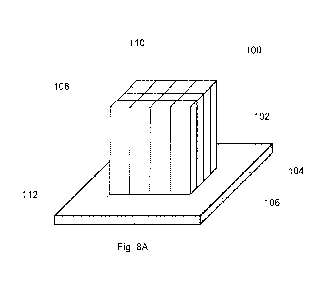
and at least
one layer overlaying the nanocables.
[0007] US 2015/0263302 discloses photovoltaic device comprising patterned
nanofibers. The
nanofiber comprises a core, which extends along the axis of the nanofiber, and
its main
component includes Ag(NH3)2 + or AgNO3; a shell, which extends along the
nanofiber
and coats the core of the nanofiber, and its main component of the shell
structure
includes: PVP, TBAP, SDS, grapheme, PMAA or PFBT nanoparticle.
[0008] US 2016/0043250 discloses three-dimensional photovoltaic devices
comprising non-
conductive cores. The photovoltaic structure disclosed in this reference
comprises a
dielectric material layer comprising a planar portion having a uniform
thickness and an
array of protruding portions extending from a planar surface of the planar
portion; and a
layer stack located on the dielectric material layer and comprising a core
conductive
material layer, a photovoltaic material layer, and a transparent conductive
material layer.
The core conductive material layer is in contact with the planar surface and
the
protruding portions of the dielectric material layer, the transparent
conductive material
2
CA 03021604 2018-10-19
WO 2017/185188 PCT/CA2017/050523
layer is spaced from the core conductive material layer by the photovoltaic
material layer
and each combination of a protruding portion of the dielectric material layer
and portions
of the layer stack surrounding the protruding portion constitutes a
photovoltaic bristle.
The basic building blocks in the device of this reference are the photovoltaic
bristles,
which also allow incident lights coming from all directions and also allow
escape of a
large portion of light without being able to participate in photovoltaic
event.
[0009] There is still a need for photovoltaic power generator structures/solar
cells which can
exhibit an improved conversion rate from solar radiations to electric power.
[0010] This background information is provided to reveal information believed
by the applicant
to be of possible relevance to the present invention. No admission is
necessarily
intended, nor should be construed, that any of the preceding information
constitutes
prior art against the present invention.
Summary of the invention
[0011] An object of the present invention is to provide three dimensional
photovoltaic structures
and a power generation apparatus comprising same.
[0012] In accordance with an aspect of the present invention, there is
provided a photovoltaic
structure, comprising: a light transmitting solid optical core having a
longitudinal axis,
having a top end, a bottom end and one or more side walls. The top end having
an
exposed outer surface to receive light. A photovoltaic layer surrounding at
least a
portion of one or more of the side walls of the optical core, and an optical
cladding layer
surrounding the photovoltaic layer.
[0013] In accordance with another aspect of the present invention, there is
provided a three-
dimensional photovoltaic power generation apparatus, comprising: a base
structure
having an upper surface and a lower surface; a plurality of photovoltaic
structures, each
having a longitudinal axis, a top end and a bottom end, and comprising: a
light
transmitting solid optical core having a top end, a bottom end and one or more
side
walls, the top end of the core having an exposed outer surface to receive
light; a
photovoltaic layer surrounding at least a portion of one or more of the side
walls of the
3
CA 03021604 2018-10-19
WO 2017/185188 PCT/CA2017/050523
optical core; and an optical cladding layer surrounding the photovoltaic
layer, wherein
the bottom end of each of the plurality of photovoltaic structures is in
direct or indirect
association with the upper surface of the base structure.
[0014] Embodiments of the present invention provide improved photovoltaic
structures to
systematically increase the ECS for a given solar cell with given surface
area, without
altering the physical and chemical properties of the semiconductor. The
photovoltaic
structures of the present invention provide increased area of ECS so that the
photons
carried in solar radiation have more opportunities to meet and interact with
the electrons
in the material. The optical core of the present invention provides an ideal
chamber to
seal the incident light inside the photovoltaic structure and increases the
likelihood of
photons interacting with the electrons of the photovoltaic layer. The presence
of optical
cladding layer further assists in increasing the ECS.
Brief description of the Figures
[0015] Fig. 1A illustrates a top view of a layered photovoltaic structure in
accordance with an
embodiment of the present invention;
[0016] Fig. 1B illustrates a top view of a layered photovoltaic structure in
accordance with an
embodiment of the present invention;
[0017] Fig. 2A illustrates a perspective view of an optical core in accordance
with an
embodiment of the present invention;
[0018] Fig. 2B illustrates a perspective view of an optical core in accordance
with an
embodiment of the present invention;
[0019] Fig. 3 illustrates a sectional view of a layered photovoltaic
structures in accordance with
an embodiment of the present invention;
[0020] Figure 4A illustrates a sectional view of the photovoltaic structures
comprising core and
a single semiconductor layer;
4
CA 03021604 2018-10-19
WO 2017/185188 PCT/CA2017/050523
[0021] Figures 4B illustrates a sectional view of the photovoltaic structures
comprising core and
multiple spectrum-selective semiconductor layers;
[0022] Figures 4C illustrates a sectional view of the photovoltaic structures
comprising core and
multiple tandem semiconductor layers with spectrum selectivity in axial and
radial
direction;
[0023] Fig. 5 illustrates a top view of the photovoltaic structure depicting
spectrum selectivity
along the circular direction in accordance with an embodiment of the present
invention;
[0024] Figs. 6A-6C illustrate different configurations of metallic layers on
the optical core in
accordance with certain embodiments of the present invention;
[0025] Fig. 6D is the top view of the embodiment of figure 6A;
[0026] Figs. 7A-7F illustrate top views of layered photovoltaic structures
comprising stuffing
layers of different shapes, in accordance with certain embodiments from the
present
invention;
[0027] Fig. 8A illustrates a perspective view of the photovoltaic power
generation apparatus in
accordance with one embodiment of the present invention;
[0028] Fig. 8B illustrates a perspective view of the photovoltaic power
generation apparatus in
accordance with one embodiment of the present invention;
[0029] Fig. 8C illustrates a perspective view of the photovoltaic power
generation apparatus in
accordance with one embodiment of the present invention;
[0030] Figs.9A and 9B illustrate top views of photovoltaic structures packed
and encased in a
base structure in accordance with certain embodiments of the present
invention;
[0031] Figs. 10A-10C illustrate top views of base structures showing shapes of
photovoltaic
structures in accordance with certain embodiments of the present invention;
CA 03021604 2018-10-19
WO 2017/185188 PCT/CA2017/050523
[0032] Figs. 11A-11G illustrate packing configurations, relative heights and
cross sectional
shapes of photovoltaic structures in accordance with embodiments of the
present
invention;
[0033] Fig. 12 illustrates the unit structure of base structure and its
integration with a
corresponding photovoltaic structure in accordance with an embodiment of the
present
invention;
[0034] Fig. 13A illustrates a photovoltaic power generation apparatus with
additional stuffing
layer between adjacent photovoltaic structures, in accordance with an
embodiment of
the present invention;
[0035] Fig. 13B illustrates a photovoltaic power generation apparatus without
additional stuffing
between adjacent photovoltaic structures, in accordance with an embodiment of
the
present invention;
[0036] Fig. 14 illustrates a photovoltaic power generation apparatus with
stuffing layer between
cone shaped photovoltaic structures;
[0037] Figs. 15A-15C illustrate electric connections inside a photovoltaic
power generation
apparatus, in accordance with an embodiment of the present invention;
[0038] Fig. 16 illustrates variations in geometric shapes of the top end of
the photovoltaic
structures, in accordance with certain embodiments of the present invention;
and
[0039] Fig. 17 illustrates an array of photovoltaic power generation apparatus
disposed on a
surface.
DETAILED DESCRIPTION OF THE INVENTION
[0040] As used herein, the term "about" refers to a +/-10% variation from the
nominal value. It
is to be understood that such a variation is always included in a given value
provided
herein, whether or not it is specifically referred to.
6
CA 03021604 2018-10-19
WO 2017/185188 PCT/CA2017/050523
[0041] As used herein, the term "geometric prism" refers to a three-
dimensional shaped
structure, for example a microstructure, having top and bottom faces connected
by flat
or curved sidewalls. This type of shape is also referred to herein as a
microprism, and
includes cylinders, cubes, cuboids, rectangular prisms, hexagonal prisms, and
the like.
In various embodiments, the top and bottom faces are parallel and are
similarly sized
and shaped. However, it is also envisioned that the structure may have
differently sized
and/or shaped top and bottom faces, for example in accordance with a frustro-
conical
shape.
[0042] As used herein, the term "conical shape" refers to a three dimensional
shaped structure
having a top face and non-parallel sidewalls tapering to a point, or tapering
to a bottom
face having a small but possibly nonzero area. The absence or reduction in
size of the
bottom face mitigates the need for a photovoltaic structure at this location.
The conical
shaped structures can have a cross section shape of circle, triangular,
square,
pentagon, hexagon, etc. Conical shaped structures may be cones, pyramids, or
the
like.
[0043] Unless defined otherwise, all technical and scientific terms used
herein have the same
meaning as commonly understood by one of ordinary skill in the art to which
this
invention belongs.
[0044] The present invention provides three dimensional photovoltaic
structures and a power
generation apparatus comprising same.
[0045] In one aspect of the present invention, there is provided a three
dimensional
photovoltaic structure, one or more of which can be used in a power generation
apparatus.
[0046] The photovoltaic structure of the present invention has a longitudinal
axis, a top end and
a bottom end, and comprises a light transmitting solid optical core having a
top end, a
bottom end and side wall(s). The photovoltaic structure further comprises a
photovoltaic
layer which surrounds the walls of the core, an optical cladding layer which
surrounds
the photovoltaic layer, and optionally an outermost stuffing layer. The top
end of the
optical core has an exposed outer surface to receive light.
7
CA 03021604 2018-10-19
WO 2017/185188 PCT/CA2017/050523
[0047] Layered Fig. lA illustrates a top view of an exemplary layered
photovoltaic structure 10a
of the present invention showing the core 12a, photovoltaic layer 14a, optical
cladding
layer 16a, and a stuffing layer 18a. Fig. 1B illustrates a top view of another
example of
the layered photovoltaic structure 10b of the present invention showing the
core 12b,
photovoltaic layer 14b, optical cladding layer 16b, and a stuffing layer 18b.
[0048] The photovoltaic layer surrounds at least a portion of at least one
(i.e. one or more) of
the sidewalls. In some embodiments the photovoltaic layer surrounds
substantially all of
at least one sidewall. In some embodiments the photovoltaic layer surrounds
substantially at least part of all of the sidewalls. In some embodiments, the
photovoltaic
layers surrounds substantially all parts of all of the sidewalls. It should be
understood
that a photovoltaic layer of larger surface area can in various embodiments
result in
greater photovoltaic activity. However, at least some photovoltaic activity
can still be
provided even when the photovoltaic layer does not surround all parts of all
sidewalls
(i.e. when there are gaps in the photovoltaic layer). Gaps can similarly be
provided in
the optical cladding layer.
[0049] In some embodiments, the sidewalls are substantially flat between their
upper end and
there lower end. In other embodiments, the sidewalls may be curved between
their
upper and lower ends. The sidewall upper end refers to the sidewall terminal
portion
which is proximate to the region of the apparatus which is exposed to light,
while the
lower and refers to the opposite side will terminal portion.'
[0050] Figs. 2A and 2B illustrate perspective view of examples of the optical
core in accordance
of the present invention, showing a top end 20a, 20b, a bottom end 22a, 22b
and side
wall(s) 24a, 24b, and an exposed top outer surface 26a, 26b to receive
incident light.
[0051] The optical core can be made of non-conductive and/or non-opaque
materials, known
for making the cores of optical fibers. In one embodiment, the optical core is
made of a
highly optically permeable material. In various embodiments, substantially the
entire
interior of the solid optical core is composed of such material.
[0052] The refractive index of the optical core and/or photovoltaic layer is
higher than the
refractive index of the optical cladding layer. In some embodiments, the
optical core has
8
CA 03021604 2018-10-19
WO 2017/185188 PCT/CA2017/050523
a refractive index greater than a refractive index of the photovoltaic layer.
In one
embodiment, the optical core has a refractive index which is approximately
equal to a
refractive index of the photovoltaic layer.
[0053] The solid optical core in the photovoltaic structures of the present
invention conducts
incident light with acceptably low or minimal loss of radiation energy, thus
making the
power generation apparatus/solar cell comprising photovoltaic structures well
adaptive
to ambient lights and scattered lights, which increases its harvest rate of
solar radiation
energy in all weather conditions of all seasons.
[0054] As depicted in Figs. 2A and 2B, the incident sunlight may come in a
variety of directions
from the top surface of the core of the photovoltaic structures. Only the
incident lights in
a direction parallel with the longitudinal axis of the photovoltaic structures
would go
through and directly hit the bottom of the structure, and most of incident
light in other
directions would hit the side walls of the photovoltaic structures before
reaching the
bottom of the structure.
[0055] The photovoltaic structures of the present invention allow a
significant portion of the
incident lights to be reflected when it penetrates through the photovoltaic
layer and hits
the optical cladding layer. This reflected light would continue to travel
through the
photovoltaic structures until they eventually reach the bottom, during which
they would
meet the walls of the photovoltaic structures a number of times, thereby
increasing the
opportunities for the photons in the light to meet and interact with the
photovoltaic
layers.
[0056] Figs. 2A and 2B illustrate paths of incident light inside the core of
the photovoltaic
structures in accordance with certain embodiments from the present invention.
As
shown in Figs. 2A and 2B, the incident light 41 upon entry into the optical
core gets
reflected back from the wall and/or bottom of the core as rays 42, 43 and 44,
thereby
increasing the opportunities for the photons in the light to meet and interact
with the
photovoltaic layers.
[0057] In some embodiments, the photovoltaic structure of the present
invention further
comprises an additional layer at or near the top end, having an anti-
reflective light
9
CA 03021604 2018-10-19
WO 2017/185188 PCT/CA2017/050523
transmitting outer surface and a highly reflective inner surface. The
additional layer has
limited or minimal impact to the incident light but can significantly reduce
the amount of
light tending to escape from the photovoltaic structure to the air. In such
embodiments,
a portion of the photons in the light are reflected back to continue to travel
within the
photovoltaic structure.
[0058] Figs. 2A and 2B show the additional layer 28a, 28b having light
transmitting outer
surface 30a, 30b, and reflective inner surface 32a, 32b, wherein the lights
rays 44 are
reflected back from the inner surface as rays 45 to continue to travel within
the
photovoltaic structure. In this example, the additional layer 28a, 28b, is
provided at a
height "h" relative to the height "H" of the optical core.
[0059] The photovoltaic structures of the present invention can have one of a
variety of shapes
such as a cylinder, a geometric prism, a cone, a pyramid, a cube, a cuboid, a
rectangle
and any combination thereof.
[0060] The cone shaped photovoltaic structures can have a variety of cross
sectional shapes
such as hexagonal, square, rectangular, circular, etc.
[0061] In Non-conical photovoltaic structures (such as geometric prisms,
cylinders, cubes, etc.),
the bottom end of optical core is also surrounded by a photovoltaic layer and
an optical
cladding layer, so that when the light photons reach the bottom, they get
reflected back
at the optical cladding layer of the bottom, after a portion of them interact
with the
photovoltaic layer at the bottom. In such embodiments, reflected light photons
would
continue to travel from bottom to the top, and may hit the walls a number of
times in the
journey and continue to interact with the photovoltaic layers on the walls. In
such
embodiments, the optical cladding layer on the walls and at the bottom of the
photovoltaic structures, together with the additional layer, form a
substantially closed
optical chamber to increase or maximize the likelihood for the incident light
to participate
in the photovoltaic interactions inside the photovoltaic structures. As a
result, the ECS is
significantly increased. Furthermore, embodiments wherein the optic core is
made of
materials with high optical permeability would ensure that the light loss when
travelling in
this chamber is mitigated or even minimized.
CA 03021604 2018-10-19
WO 2017/185188 PCT/CA2017/050523
[0062] An example of such an embodiment is depicted in Fig. 3, which
illustrates a sectional
view of a photovoltaic structure showing optical core 52, photovoltaic layer
54 and
optical cladding layer 56, both surrounding the walls and bottom of a
cylindrical core.
The top end of the optical core in this example also has an additional layer
58 having
anti-reflective light transmitting outer surface and a highly reflective inner
surface.
[0063] In case of conical photovoltaic structures the bottom end is defined by
the apex or vertex
of the cones. In such embodiments, the light-sealing chamber is formed by the
walls of
the cones and the additional layer at the top. However, in this case the
bottom portion
of the structure is reduced to a point, or nearly a point, and the sidewalls
of the structure
are non-parallel, thereby changing the paths of incident and reflected light.
[0064] The photovoltaic layer is where the photovoltaic conversion takes
place. In some
embodiments, the photovoltaic layer comprises a multi-layer structure.
[0065] In some embodiments, the photovoltaic layer comprises an interior
metallic layer in
contact with the optical core, one or more conductive layers surrounding the
interior
metallic layer, and an outer metallic layer surrounding the one or more
conductive
layers.
[0066] Fig. 3 shows an example of the photovoltaic layer 54 comprising an
interior metallic
layer 60 in contact with the optical core 52, a conductive layer 62
surrounding the
interior metallic layer 60, and an outer metallic layer 64 surrounding the
conductive layer
62.
[0067] In some embodiments, the one or more conductive layers are
semiconductor layers,
(also referred to as PN junction layers), comprising one or more PN junctions.
The PN
junctions are configured to generate an electrical voltage in response to
photonic
bombardment and penetration, in accordance with a photovoltaic effect.
[0068] In some embodiments, the photovoltaic layer comprises one semiconductor
layer/PN
junction layer with its associated interior metallic layer and exterior
metallic layer. In
some embodiments, the photovoltaic layer comprises a plurality of
semiconductor layers
11
CA 03021604 2018-10-19
WO 2017/185188 PCT/CA2017/050523
/PN junction layers, each with their own respective interior metallic layers
and exterior
metallic layers.
[0069] Fig. 4A illustrates a sectional view of an exemplary photovoltaic
structure comprising
optical core 70 and photovoltaic layer 72 comprising one PN junction 76
between inner
metallic layer 74 and outer metallic layer 78. Figs. 4B and 4C illustrate
examples
wherein the photovoltaic layer comprises a plurality of semiconductor layers
/PN junction
layers 76 each with their own respective interior metallic layer 74 and
exterior metallic
layer 78.
[0070] In this disclosure, a semiconductor layer/PN junction layer is referred
to as a
semiconductor structure formed by two types of semiconductor material, p-type
and n-
type. Candidate materials and processes for the implementation of the PN
junction
layers are well known in the art. Suitable material ranges from silicon to non-
silicon
elements or compounds. In a typical embodiment one may choose thin-film solar
cell
materials such as amorphous silicon (a-Si), micro-crystalline silicon (pc-Si),
or nano-
crystalline silicon (nc-Si). In some embodiments, a PN junction layer may be
understood
as a P-I-N layer where "I" is meant to be an intrinsic semiconductor layer.
[0071] Depending on the polarity of the PN junctions (i.e. the relative
locations of the positively
and negatively doped semiconductor regions) in the photovoltaic layer in any
specific
embodiment, the activated electrons may move towards the direction of optical
core, or
towards the direction of optical cladding layer, when a photovoltaic
interaction takes
place. In one embodiment, the electrons move toward the direction of the
optical core
when a photovoltaic event takes place.
[0072] In some embodiments, solar radiation spectrum-selectivity is considered
when choosing
different materials for implementing the photovoltaic layer for the
photovoltaic structures
of the present invention. While some materials are best tuned to absorb solar
energy
carried by shorter wavelength photons, some other materials are best tuned to
react to
longer wavelength photons. The three-dimensional structural nature of the
photovoltaic
structures provides a possibility of optimizing spatial distribution of
semiconductor
materials along the circular, axial, and/or radial dimensions.
12
CA 03021604 2018-10-19
WO 2017/185188 PCT/CA2017/050523
[0073] By applying photovoltaic materials that are best tuned to different
wavebands of light to
different segments of the photovoltaic structure, one can obtain the spectrum
selectivity
along the axial direction. An approach in one embodiment is to apply an
amorphous
silicon coating to the upper part of the photovoltaic structure (microprism or
micro-cone)
with best spectrum response to green and blue lights wavelengths, and to apply
certain
pc-Si or nc-Si coating to the lower part of the microprism or micro-cone with
best
spectrum response to red and infrared wavelengths. Depending on particular
considerations a designer can play with this axial spectrum selectivity in a
variety of
ways in different embodiments.
[0074] By overlaying photovoltaic materials that are best tuned to different
wavebands of light
on successive coating layers surrounding the optical core, one can obtain a
photovoltaic
structure with spectrum selectivity along the radial direction. An approach in
one
embodiment is to mimic the tandem PN junctions configuration that has been in
industry
practice for years, where an amorphous silicon coating is first applied with
best
spectrum response to green and blue light wavelengths, and then a pc-Si or nc-
Si
coating is overlaid on top of amorphous silicon coating with best spectrum
response to
red and infrared wavelengths.
[0075] By applying photovoltaic materials that are best tuned to different
wavebands of light to
different segments of the same photovoltaic coating layer, one can obtain a
photovoltaic
structure with spectrum selectivity along the circular direction. An approach
in one
embodiment is to apply an amorphous silicon coating to one half side of the
microprism
or micro-cone, with best spectrum response to green and blue lights
wavelengths, and a
pc-Si or nc-Si coating to the other half side of the microprism or micro-cone,
with best
spectrum response to red and infrared wavelengths.
[0076] Fig. 4B illustrates multiple spectrum-selective semiconductor/PN
junction layers, and
Fig. 4C illustrates multiple tandem semiconductor layers with spectrum
selectivity in
axial and radial direction. Different shades in these exemplary drawings
represent
photovoltaic materials best tuned to different wavebands of solar radiation
spectrum.
[0077] Figs. 5A and 5B illustrate spectrum selectivity along the three
dimensions, wherein Fig.
5A illustrates spectrum selectivity in axial and radial directions, and Fig.
5B illustrates a
13
CA 03021604 2018-10-19
WO 2017/185188 PCT/CA2017/050523
top view of an example of the photovoltaic structure depicting spectrum
selectivity along
the circular direction, wherein the optical core 80 is surrounded by interior
metallic layer
82. The photovoltaic layer has a photovoltaic coating 86 best tuned to short
wavebands,
a photovoltaic coating 88 best tuned to long wavebands. The photovoltaic layer
is
surrounded by the optical cladding layer 84.
[0078] The functions of the interior metallic layer and an exterior metallic
layer associated with
each conductive layer are to capture and collect the electrons (or holes) in
the
conductive layer that are displaced into the metallic layers as a result of
the photovoltaic
interaction, and to provide a cathode (anode) electrical connection for the
photovoltaic
structure, for example to electrically connect with other photovoltaic
structures of the
same cell. The terms "interior" and "exterior" are meant in respect to the
optical core:
when the light travels from the optical core to the optical cladding layer, it
first meets the
interior metallic layer of each conductive layer, then the conductive layer
itself, and then
the exterior metallic layer. On the other hand, when the light travels from
the optical
cladding layer to the optical core, it first meets the exterior metallic layer
of each
conductive layer, then the conductive layer itself, and then the interior
metallic layer.
The photovoltaic layer typically includes electrical connections such as
probes,
conductive traces or wires which are electrically coupled to the metallic
layers. The
electrical connections of multiple photovoltaic structures can be connected in
series
and/or parallel to provide direct current electrical power, as would be
readily understood
by a worker skilled in the art.
[0079] The interior metallic layer and exterior metallic layers are made of
materials with high
optical permeability and/or with good electric conductivity. In some
embodiments, ITO
(Indium Tin Oxide) and TCO (transparent conductive oxide) can be good
candidate
materials to implement these metallic layers.
[0080] The metallic layers may cover the entire height of the photovoltaic
structures, or from the
bottom up to the level "h" where the additional layer having anti-reflective
outer surface
is placed.
[0081] Figs. 6A to 6C illustrate examples of different configurations of
metallic layers on a
optical core 90. Fig. 6D is the top view of Fig. 6A, showing optical core 90
surrounded
14
CA 03021604 2018-10-19
WO 2017/185188 PCT/CA2017/050523
by photovoltaic layer 92 having inner metallic layer 94, PN junction layer 96
and outer
metallic layer 98.
[0082] The function of the optical cladding layer is to make the photovoltaic
structures a good
chamber for containing the incident light inside the photovoltaic structures
so as to
increase or even maximize the area of photovoltaic ECS. Its index of
refraction is
smaller than the refraction indices of all the other layers and of the optical
core.
[0083] Fig.3 shows an example of optical propagation inside the non-conical
shaped
photovoltaic structure (such as a microprism, cylinder, cube, etc.)¨the life
of photons
when a beam of incident light enters the photovoltaic structure. Photon w
takes part in a
photovoltaic event and successfully contributes to activation of an electron.
Photon x
penetrates the photovoltaic layer, gets bounced (reflected) back at the
optical cladding
layer, re-enters the photovoltaic layer and the optical core, and lands at the
photovoltaic
layer at the bottom of the photovoltaic structure where it contributes to a
photovoltaic
event. Photon y hits the optical cladding layer three times: once on the left
wall, once at
the bottom, and once on the right wall, and finally lands at the photovoltaic
layer on the
right wall of the microprism. Photon z lands at the photovoltaic layer on the
left wall of
the microprism after it hits the optical cladding layer three times and then
gets bounced
back at the top by the antireflection layer.
[0084] The similar principle applies to cone shaped photovoltaic structures.
In case of conical
photovoltaic structures the bottom end is defined by the apex or vertex of the
cones. In
such embodiments, the light-sealing chamber is formed by the walls of the
cones and
the additional layer at the top. However, in this case the bottom portion of
the structure
is reduced to a point, or nearly a point, and the sidewalls of the structure
are non-
parallel, thereby changing the paths of incident and reflected light.
[0085] The cross sectional shapes of the optical core, the photovoltaic layer,
the optical
cladding layer and the stuffing layer can be same or different. In one
embodiment, the
cross sectional shape of the optical core, the photovoltaic layer, and the
optical cladding
layer is same (i.e. Figs. 7A and 7F). In some embodiments, the cross-sectional
shape
of the photovoltaic layer and the optical cladding layer is different than the
optical core
(Figs. 7B, 7C, 7D and 7E).
CA 03021604 2018-10-19
WO 2017/185188 PCT/CA2017/050523
[0086] In another aspect of the present invention, there is provided a three
dimensional
photovoltaic power generation apparatus comprising a plurality of photovoltaic
structures
of the present invention as described above. The power generation apparatus
comprises a base structure having an upper surface and a lower surface,
wherein the
lower surface is in direct or indirect association with the bottom end of each
of the
photovoltaic structures. In one embodiment, the photovoltaic power
generation
apparatus is a solar cell.
[0087] Fig. 8A illustrates an exemplary three dimensional photovoltaic power
generation
apparatus 100 comprising a base structure 102 having an upper surface 104 and
a
lower surface 106, and a plurality of photovoltaic structures 108 each having
a top end
110, a bottom end 112. The bottom end 112 of each of the photovoltaic
structures is in
direct or indirect association with the upper surface 104 of the base
structure.
[0088] In some embodiments, the base structure comprises side wall(s) 114 to
encase the
plurality of the photovoltaic structures (Figs. 8B and 8C).
[0089] In some embodiments the side walls wrap all photovoltaic structures
together like a solid
'brick'.
[0090] In some embodiments, the photovoltaic structures can be packed together
with gluing
materials, and there may or may not be a case that contains all of the
photovoltaic
structures in a cell.
[0091] The three dimensional photovoltaic power generation apparatus/solar
cell viewed from
top can have a variety of geometrical shapes such a rectangular, square,
triangle,
hexagonal, etc. (for example as shown in Figs. 9A, 9B, 10A, 10B and 10C, or
any other
shape).
[0092] The heights of all photovoltaic structures in a photovoltaic power
generation
apparatus/solar cell can be the same as shown in Figs.11A, 11C, 11D, 11G, and
11E or
can be different as shown in Figs. 11B, 11F, and 11H.
16
CA 03021604 2018-10-19
WO 2017/185188 PCT/CA2017/050523
[0093] Although in various illustrated embodiments the bottom face of the non-
conical
photovoltaic structures is flat, it is possible that the bottom face may be
curved. For
example, the structure may be hemispherical in shape.
[0094] In some embodiments, the upper surface of the base structure has a
plurality of
receiving structures shaped to accommodate the shape of the bottom of a
corresponding photovoltaic structure.
For example, in the case of non-conical
photovoltaic structures (such as microprisms), the base structure seals the
bottoms of
all photovoltaic structures of the same cell with all functions that are
provided by the
walls of the photovoltaic structures (Fig.12).
[0095] In some embodiments, the photovoltaic layer and the cladding layer
surround the bottom
end of the optical core. In some embodiments of non-conical photovoltaic
structures
(such as microprisms, cube, etc.), the portion of the photovoltaic layer and
the cladding
layer surrounding the bottom end of the optical core is integral to the base
structure.
For example, referring to a microprism shaped photovoltaic structure, the base
structure
contains a plurality of units each of which connects to one and exactly one
microprism
that stands on it. The base structure is prepared with all the units having
exactly the
same layered structure as the walls of the microprisms, that is, a
photovoltaic layer
which may contain a plurality of PN junction layers and their associated
metallic layers,
and an optical cladding layer as the outermost layer. The one-to-one
correspondence of
these layers of the base structure with the layers of the walls makes a
seamless
encapsulation around the optic core of the microprisms, leaving only the top
open with
an antireflection layer slightly underneath the top (for example as shown in
Figs. 2A and
2B). The photovoltaic layer and the optical cladding layer portions of both
the base
structure and the photovoltaic structure are aligned so as to provide
contiguous layered
structures.
[0096] Fig. 12 illustrates an exemplary receiving structure 208 of base
structure 202 having
upper surface 204 and lower surface 206, and its integration with a
corresponding
photovoltaic structure 210 . In this example, the receiving structure has an
internal
metallic layer 212, PN junction layer 214, external metallic layer 216, and
optical
cladding layer 218, each of which correspond to their respective layers of the
17
CA 03021604 2018-10-19
WO 2017/185188 PCT/CA2017/050523
corresponding photovoltaic structure 210 (i.e. an internal metallic layer 222,
PN junction
layer 224, external metallic layer 226, and optical cladding layer 228).
[0097] In the embodiments comprising cone shaped photovoltaic structures there
is no such
step of bottom processing.
[0098] As discussed above, the photovoltaic structures of the present
invention optionally
comprise a stuffing layer surrounding the optical cladding layer. The
plurality of
photovoltaic structures can be assembled with or without an additional
stuffing layer
between the assembled photovoltaic structures.
[0099] In one embodiment, non-conical photovoltaic structures are assembled
with or without
an additional stuffing layer. In one embodiment, conical photovoltaic
structures are
assembled with an additional stuffing layer.
[00100] The function of the stuffing layer is to provide the power
generation
apparatus/solar cell with mechanical features (such as load bearing) or
operational
features (such as sensor) as desired or required.
[00101] Fig. 13A illustrates an example of the power generation
apparatus/solar cell with
additional stuffing layer 312 between adjacent non-conical photovoltaic
structures 310.
Fig. 13B illustrates an example of power generation apparatus/solar cell
without
additional stuffing between adjacent non-conical photovoltaic structures.
[00102] Fig. 14 illustrates an exemplary power generation apparatus/solar
cell with an
additional stuffing layer 412 between cone shaped photovoltaic structures 410.
[00103] In some embodiments, for the case of cone shaped photovoltaic
structures, a
stuffing layer is provided in order to make a rectangular 3-D solar cell.
[00104] The power generation apparatus of the present invention also
comprises
electrical wiring and connections to convert the energy of light into
electricity by the
photovoltaic effect. The electrical wiring and connections are as known in the
art.
18
CA 03021604 2018-10-19
WO 2017/185188 PCT/CA2017/050523
[00105] Figs. 15A to 15C illustrate schematic depiction of electrical
wirings inside a power
generation apparatus/solar cell of the present invention. Fig, 15A shows a
pair of DC
connection wires coming out of each photovoltaic structure. The photovoltaic
structures
of the same power generation apparatus/solar cell are electrically connected
in parallel
(Fig.15B) to collect tiny electric currents resulting from the photovoltaic
effects of all
photovoltaic structures. As a result of such integration, a finished solar
cell is seen from
outside to have one positive electrode and one negative electrode (Fig.15C).
[00106] The top ends of all photovoltaic structures are directly exposed to
the sunlight,
and therefore the power generation apparatus/solar cells have one side that
receives
the solar radiation, for example as shown in Fig. 17. In certain embodiments
for certain
purposes, the tops maybe processed into different geometric shapes, and may be
coated with a thin anti-dust film.
[00107] Finished power generation apparatus of the present invention can be
used in a
wide range of applications, for example to construct pavements on virtually
any
surfaces. Fig.18 illustrates an array of power generation apparatus/solar cell
disposed
on a surface.
[00108] In another aspect of the present invention there is provided a
systematic method
to significantly increase the ECS for a given solar cell with given surface
area.
[00109] It is obvious that the foregoing embodiments of the invention are
examples and
can be varied in many ways. Such present or future variations are not to be
regarded
as a departure from the spirit and scope of the invention, and all such
modifications as
would be obvious to one skilled in the art are intended to be included within
the scope of
the following claims.
19