Note: Descriptions are shown in the official language in which they were submitted.
CA 03021704 2018-10-22
TiCN having reduced growth defects by means of HiPIMS
The invention relates to a method for applying a TiCN coating with reduced
growth
defects to surfaces, in particular the surfaces of workpieces, components or
tools.
Prior art
When coating using reactive sputter or HiPIMS processes, a metallic target is
often
used as the source of the vapor deposition material and at least one reactive
gas is
used in addition to the process gas. Within the scope of the present
invention, the
terms "vapor deposition" and "sputtering" are considered identical. That
component cf
a sputter source from which material is stripped during the process is
designated the
target within the scope of the present invention.
For depositing layers using reactive sputter processes or also using cathodic
arc
deposition, two reactive gases are usually needed. According to prior art,
these are
usually nitrogen and a gas containing carbon, usually acetylene (C2H2). While
arc
deposition can be considered a relatively robust process, regulating the
process gas
plays a crucial role for process stability, in particular for the sputter or
HiPIMS
processes.
Krassnitzer discloses, in W02014207154 for example, a method for depositing
TiCN
layers using HiPIMS wherein sputtering is used on Ti targets in a reactive
atmosphere
containing N2 and C2H2 to apply TiCN layers to substrate surfaces. The HiPIMS
process uses power pulses and/or power pulse sequences with an energy content
referenced to the target area of at least 0.2 joules/cm2 per power pulse or
power pulse
sequence. It is proposed to control the concentration of the reactive gases in
the
coating chamber by regulating or controlling the reactive gas flows arid to
control
various properties such as the color impression by means of the concentration
of the
reactive gases in the coating chamber.
It is known that, during the sputter or HiPIMS process, the two reactive gases
react
with the vaporized target material and form a metal-ceramic layer on the
substrate. To
Page 1 of 15
CA 03021704 2018-10-22
dersify the layer, a negative bias voltage is applied to the substrate to
accelerate the
positively charged ions to the substrate.
It is also known that, to set optimum layer properties in a repeatable manner,
precise
knowledge and control of a sputter or HiPIMS process is extremely important.
In this
respect, the choice of the optimum operating point can be considered
especially crucial
because even a slight deviation from this operating point during the process
can lead
to fluctuations in the layer quality, changed color properties, process
instability and
finally to a process breakdown. The term operating point here designates a
specific
ratio of the process gas to the one or plurality of reactive gases.
To keep a selected operating point constant during the process, a gas flow or
partial
pressure control system is usually used. This means, with only one reactive
gas, for
example, when depositing TiN, an Ar partial pressure of 0.40 Pa and an N2
partial
pressure of 0.03 Pa are set, resulting in a total pressure of 0.43 Pa. In a
HiPIMS
process, the operating point can be very dependent on the selected process
conditions
such as the averaged pulse power, P., or the pulse duration, but
also on the
state and age of the target used or the pump power. The set operating point,
the N2
par:ial pressure or the total pressure resulting from this is usually achieved
by changing
the flow of N2.
However, if two or a plurality of reactive gases such as N2 and C2H2 are used
at the
same time, this concept can no longer be applied because the pressure of only
one
reactive gas can be controlled and the other reactive gas is usually admitted
into the
chamber at a fixed flow rate.
For the reasons cited above, it can be seen that slight changes to the process
parameters result in a deviation from the desired operating point, a situation
that can,
in turn, have a negative impact on the desired layer quality.
The problems cited above play a decisive role, in particular during the
reactive
deposition of TiCN wherein the two elements of carbon and nitrogen are
stripped from
the gas phase and react with the titanium sputtered from the titanium target
to form
TiCN. Even slight deviations of the optimum operating point can cause
considerable
deviations of the layer properties.
Page 2 of 15
CA 03021704 2018-10-22
Another critical aspect of reactive sputter or HiPIMS processes is the
reaction of one
or a plurality of reactive gases with the target surface, which usually forms
ceramic
reaction products. In general, this process is known as target poisoning and
can have
considerable effects on the sputter characteristic or the operating point of a
process. If
poorly conducting or even insulating compounds form on the target surface
during
target poisoning, this may lead to a drastic increase of the discharge voltage
and, in
the worst case, cause a collapse of the sputter plasma if the entire target
surface is
covered.
In EP2565291A1, ills proposed to avoid the phenomenon of target poisoning when
using reactive sputter processes with different target materials in that a gas
flow
controller is attached to the sputter source, said controller setting the flow
of reactive
gas depending on the magnitude of the poisoning on the corresponding sputter
target,
this determination being made by measuring the source voltage and, according
to a
preset target value, allowing control of the flow of reactive gas. However,
this method
is relatively expensive to implement and requires detailed knowledge of the
processes
at the target in conjunction with the reactive gases. In addition, it is not
possible to
select a desired operating point using the ratio of the process gas to the
reactive gas.
As a result, it is of primary importance to have a method wherein, depending
on the
desired layer properties, it is also possible to select any operating point
necessary for
this and to operate this process in a stable manner. The present invention
enables
precisely this step.
To densify the layer, a negative bias voltage is applied to the substrate to
accelerate
the positively charged ions to the substrate. When depositing layers using a
reactive
sputter or HiPIMS process with a direct current (DC) bias voltage, the voltage
used
should be greater than the plasma potential. Usually, a DC bias voltage
greater than -
V, thus -40 V for example, is applied to accelerate the ions to the substrate
material.
By increasing the DC bias voltage from -40 V to -80 V, for example, an
increase in ion
30 energy is achieved and this manifests itself in a greater density of the
layer and,
usually, in an increase in the internal stresses of the layer. Often, an
increase in the
layer hardness can also be observed with an increase in the internal stress.
Page 3 of 15
CA 03021704 2018-10-22
However, while great hardness is desired in many applications, increasing the
internal
stresses at the same time may result in considerable difficulties in achieving
the
desired layer thickness of a few micrometers at the desired location of the
component
or the tool. Internal stresses in the layer that are too high result in layer
spalling at
points or even over wide areas.
In conventional sputter or HiPIMS processes, the layer growth incorporates
growth
defects.
When producing TiCN using conventional sputter or HiPIMS processes, growth
defects
are incorporated during layer growth and these defects can, for example, come
from
metallic particles of the target that are not completely covered by the vapor
deposition
or even from impurities in the system. In addition, it is difficult to
differentiate where
exactly the vapor deposited target material reacts with the reactive gas(es)
meaning
that TiCN that has undergone a complete reaction already may be present on the
target
surface of a titanium target, this material is then vapor deposited as
"microparticles"
and can be incorporated as a growth defect in the layer growing on the
substrate. This
process of reaction by the reactive gases with the target material on the
target surface
is normally known as "poisoning" and is highly dependent on the process
parameters
and, in this case in particular, on the control of the reactive gas flow. A
target is
considered completely poisoned once the target surface has been totally
covered by
one or a plurality of reaction products.
In addition, a high surface quality of the layer on the substrate often
depends on the
layer thickness because even smaller growth defects during layer growth result
in a
considerable increase in the roughness of the coated component or tool. This
means
that thicker layers tend to exhibit greater roughness than would be the case
for a
thinner layer with the same deposition conditions.
Object of the present invention
Page 4 of 15
CA 03021704 2018-10-22
The object of the present invention is to provide a method enabling the
production of
TiCN layers with fewer growth defects but, at the same time, leading to no
loss of layer
hardness or no increase in the internal stresses of the layer if at all
possible.
It is desirable that the inventive method exhibits a high process stability.
Means of attaining the object by the present invention
According to the invention, a coating having at least one TiCN layer is
applied to a
surface of a substrate to be coated by means of HIPIMS, wherein, to deposit
the at
least one TiCN layer, at least one target containing Ti, for example, a Ti
target, is used
as the Ti source for producing the TiCN layer, said target being sputtered in
a reactive
atmosphere by means of a HiPIMS process in a coating chamber, wherein, to
reduce
growth defects during the deposition of the at least one TiCN layer, the
reactive
atmosphere comprises one inert gas, preferably argon, and at least nitrogen
gas as
the reactive gas and wherein, to reduce growth defects during deposition of
the at least
one TiCN layer,
- the reactive atmosphere additionally contains, as a second reactive gas, a
gas
containing carbon, preferable CH4, used as the source of carbon to produce the
TiCN layer wherein, while depositing the TiCN layer, a bipolar bias voltage is
applied to the substrate to be coated,
Or
- at least one target containing carbon, for example, a graphite
target, is used as
the source of carbon for producing the TiCN layer, said target being used for
sputtering in the coating chamber using a HiPIMS process with the reactive
atmosphere having only nitrogen gas as the reactive gas, wherein the targets
containing Ti, are operated preferably by means of a first power supply device
or a first power supply unit and the targets containing graphite are operated
with
pulsed power preferably by means of a second power supply device or a second
power supply unit.
Page 5 of 15
Date recue/Date received 2023-04-06
CA 03021704 2018-10-22
Description of the invention
The inventors have found that it is surprisingly possible to produce layers of
hard
material made of TiCN with a very high hardness and, at the same time, a very
smooth
layer surface with relatively low internal stresses by means of reactive
HiPIMS
processes if a bipolar bias voltage is used during the HiPIMS process. The
inventors
have also found that it is surprisingly possible to produce layers of hard
TiCN material
with a very high hardness and, at the same time, a very smooth layer surface
by means
of reactive HiPIMS processes if only nitrogen is used as the reactive gas in
the HiPIMS
process and the carbon for producing TiCN is provided by a target containing
carbon.
In this way, it is possible to grow thicker layers and to overcome the
problems cited
above, for example, in the application area, to produce a sufficiently thick
layer with
high surface quality, thus low roughness.
To deposit the TiCN layers according to the invention, a HiPIMS method was
used that
applies very high power pulses or power pulse sequences to the target surface
of one
or a plurality of titanium targets. During the pulse duration, t
-pulse, of a power pulse or
during a sequence duration, tpulsesequence, of a power pulse sequence, energy
is
introduced into the target surface by means of positively charged Ar ions that
knock
loose or vaporize target material. In a HiPIMS method, the amount of ionized
vapor
deposition material is considerably greater than in the conventional sputter
method.
The energy content in the HiPIMS process can be achieved very simply by
setting an
appropriately high pulse power, P, and/or an appropriately very long pulse
length or
pulse duration, t
-pulse.
Standard HiPIMS configurations and coating parameters are known from prior
art.
Within the scope of the present invention, such HiPIMS methods as, for
example,
described by Krassnitzer in W02012143091A1, in particular, were used.
Page 6 of 15
CA 03021704 2018-10-22
The invention is completed in detail in the following and using figures and
tables with
examples.
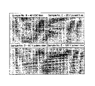
Fig. 1: Table with an overview of the properties of sample deposited TiCN
layers that
were deposited using a bipolar bias voltage according to Example 1 (see C, D,
E)
compared to TiCN layers that were deposited using a DC voltage according to
prior art
(see A, B)
Fig. 2: Light-microscope pictures of TiCN layer surfaces according to Example
1 using
different bias voltages
Fig. 3: Table with an overview of the properties of sample deposited TiCN
layers that
were deposited using Ti and graphite targets according to Example 2 (see A, B,
C, 0,
E) compared to TiCN layers that were deposited using only Ti targets and a DC
voltage
according to prior art (see REF))
Fig. 4: Light-microscope pictures of TiCN layer surfaces according to Example
2 using
different target or reactive gas configurations.
Example 1 (according to a first preferred embodiment):
All TiCN layers shown as examples for this first Example were produced with a
thin
TiN layer as the undercoat. First, the TiN undercoat was deposited on the
surface to
be coated using the following parameters: a pulse power, P
= pulse, of 60 kW, an average
power on the target, Pav, of 9.0 kW with a t -pulse of 25 ms, at a total
pressure, ptot, of 0.81
Pa, with an N2 partial pressure of 0.01 Pa, an Ar partial pressure of 0.4 Pa
and a
constant bias voltage of -80 V at a coating temperature of 450 C.
The TiCN layers were then applied immediately afterward with the same Ppuise,
the
same Pay, the same N2 partial pressure and Ar partial pressure but with an
additionally
constant CH4 flow of 50 sccm and a shorter tpulse Of 1 ms.
For the comparison examples A and B in the table of Figure 1, there was a DC
bias
voltage both during deposition of the TiN undercoat and during the deposition
of the
TiCN layer.
For the Examples C, D and E of the invention in Table 1 of Figure 1, the bias
voltage
according to the invention was changed after the deposition of the TiN
undercoat to
bipolar pulsed operation for the deposition of the TiCN layers according to
the
invention.
Page 7 of 15
CA 03021704 2018-10-22
All layers had a layer thickness of about 4.0 pm and were then characterized
as can
be seen in the summary of layer properties in Table 1. The sample numbers A
and B
were deposited under identical conditions but in different batches with a
constant DC
bias voltage of -40 V. The sample numbers C, D and E were deposited using a
bipolar
pulsed voltage of -50 V, -80 V and -100 V, respectively. The duty cycle
tneg:tpos of the
negative bias voltage to the positive bias voltage was kept constant at 50:25
ms for the
samples C, D and E.
Surprisingly, a considerable reduction in the roughness factors Ra, Rz and
Rmax was
found using pulsed bias voltage according to the invention instead of a DC
bias voltage
when the bias voltage was comparable and even higher. Figure 1 shows light-
microscope pictures of the coated sample surfaces with sample B (constant -40
V ¨
DC) being compared to the samples C, D and E. The optical impression of the
black
spots is produced by growth defects that disturb the otherwise very smooth
surface
structure under incident light. A lower density of black spots can clearly be
seen in the
samples C to E compared to sample B, something that agrees well with the
measured
roughness values. Interestingly, however, the measured carbon content of the
layers,
within the specified measuring accuracy, is independent of the method used to
apply
the bias voltage and was roughly constant at 10+2 at%.
Surprisingly, considerably lower internal stress values were measured for the
TiCN
layers using pulsed bias voltage than for the comparison samples using DC bias
voltage. As seen in Table 1, the internal stress level of -4.4 GPa that
occurred when
using -40 V of DC bias voltage was not reached until the pulsed bias voltage
was -100
V.
Furthermore, a moderate increase in the hardness was seen with the pulsed bias
voltage, a situation that is becoming more desirable for the application.
Preferably, a bias voltage in the range of -20 V to -200 V is used.
Preferably, the duty cycle tneg:tpos of the negative bias voltage to the
positive bias
voltage is in a range from 10:1 to 1:5, preferred in 5:1 to 1:2 and
particularly preferred
in 2:1 to 1:1.
Page 8 of 15
CA 03021704 2018-10-22
The bias voltage level can be set such that it is symmetrical or asymmetrical.
In the
case of asymmetrical operation, it is possible to set the ion current and the
electron
current independent of one another.
Preferably, acetylene (C2H4) or methane (CH4) is used as the gas containing
carbon.
According to another embodiment of the invention, ceramic TIC targets or
targets made
of Ti and TiC can be used in place of metallic titanium targets when
depositing TiCtsl
layers.
Example 2 (according to a second preferred embodiment):
All TiCN layers shown as examples for this second Example were produced with a
thin
TIN layer as the undercoat. First, the TiN undercoat was deposited on the
surface to
be coated using the following parameters: a pulse power, Ppuise, of 60 kW, an
average
power on the target, Pay, of 9.0 kW with a t
-pulse Of 25 ms, at a total pressure, ptot, of 0.81
Pa, with an N2 partial pressure of 0.01 Pa, an Ar partial pressure of 0.4 Pa
and a
constant bias voltage of -80 V at a coating temperature of 450 C.
During this, three titanium targets were operated in the manner specified
above.
The TiCN layers (A, B, C, D, E in the table of Fig. 3) were deposited in
accordance
with the invention immediately afterward wherein the three titanium targets
were
operated as before with the same settings but, in addition, three carbon
targets were
added.
The three carbon targets were used for deposition in different sample
processes with
Ppulse of 60 kW, a constant bias voltage of -50 V, but different tpuise values
of 0.05, 0.1,
0.2, and 0.3 ms, respectively, with the resulting Pay of 0.4, 0.9, 1.8, and
2.8 kW,
respectively. The associated samples are listed in the sequence as A, B, C and
D, and
the properties are specified in Figure 3.
As the reference sample (REF), a conventionally deposited TiCN layer was
produced,
again with the same TIN undercoat as described above wherein, however, only
titanium targets were used for the TiCN layer and Ar was used as the process
gas at
a partial pressure of 0.40 Pa, N2 was used as the first reactive gas at a
partial pressure
of 0.01 Pa and additionally CH4 was used as the second reactive gas at 50
sccm,
corresponding to a total pressure pm of 0.47 Pa. A DC bias voltage was used
both for
deposition of the TIN undercoat and for deposition of the TiCN layer. These
settings
Page 9 of 15
CA 03021704 2018-10-22
for the reference sample correspond to prior art as mentioned above in the
introduction
and serve for comparison purposes with regard to layer properties and process
stability.
A process with the TiN undercoat described above but using to process gases
and two
types of targets for the TiCN layer was used for the additional comparison
sample E.
In this case, the parameters for the three titanium targets were held constant
as
described above and the settings for the three carbon targets were comparable
to
those used for sample C, each with Ppulse of 60 kW, a constant bias voltage of
-50 V,
tr,ulse of 0.2 ms, and the resulting Pay of 1.8 kW, an Ar partial pressure of
0.4 Pa, an N2
partial pressure of 0.03 and a fixed CH4 flow of 10 sccm were used for
deposition.
All layers shown as examples had a layer thickness of about 4.0 pm and were
then
characterized as can be seen in the summary of layer properties in Table 1 of
Figure
Figure 4 shows light-microscope pictures of the coated sample surfaces with
sample
REF being compared to the samples A, B, C and D. The optical impression of the
black
spots is produced by growth defects that disturb the otherwise very smooth
surface
structure under incident light. Surprisingly, the samples A to D exhibit a
lower density
of black spots in comparison to sample REF, something that agrees well with
the
measured roughness values. The amount of carbon increases with increasing
power
at the target.
Interestingly, however, it was found that, when comparing samples REF and C,
they
both have roughly the same carbon content but a considerably higher layer
hardness
was measured for sample C with the deposition performed in accordance with the
invention. This means that using two target materials, one being titanium and
the
second, in this example, being carbon, has a positive effect on the layer
properties
and, in addition, permits a stable process.
The comparison sample E that used the two different target materials of
titanium and
carbon, and N2 and CH4 as the reactive gases, exhibits a considerably higher
surface
roughness, a fact that, however, in comparison to the linear correlation of
carbon
content or roughness of the samples A, B, C and D that used the deposition
process
of the invention, may have something to do with the high carbon content in
sample E.
Page 10 of 15
CA 03021704 2018-10-22
Within the scope of the invention, it is conceivable that a fine adjustment of
the carbon
content can be achieved by using targets made of a compound material
containing
carbon. This could be a compound, for example, that consists of one or a
plurality of
metals and one or a plurality of carbides, for example, a target made of TiC
or Ti+TiC.
It is just as conceivable that other metals such as Cr, Zr, Ta or Nb be used
for the
method according to the invention.
Preferably, a bias voltage in the range of -20 V to -200 V, a total pressure
ranging from
10-4 mbar (0.02 Pa) to 10-2 mbar (2 Pa), a power density in the range of 0.1
kw/cm2 to
3.0 kW/cm2 and/or an average power Pay in the range of 0.05 to 10 kW are used.
The
partial pressure ratio of Ar to N2 can vary within the range of 0.01 to 0.95.
Preferably, acetylene (C2H4) or methane (CH4) is used as the gas containing
carbon.
According to another embodiment of the invention, ceramic TiC targets or
targets made
of Ti and TiC can be used in place of metallic titanium targets when
depositing TiCN
layers.
Specifically, the present invention discloses a method of applying a coating
having at
least one TiCN layer to a surface of a substrate to be coated by means of
HiPIMS,
wherein, to deposit the at least one TiCN layer, at least one target
containing Ti is used
as the Ti source for producing the TiCN layer, said target being sputtered in
a reactive
atmosphere by means of a HiPIMS process in a coating chamber, wherein, to
reduce
growth defects during the deposition of the at least one TiCN layer, the
reactive
atmosphere comprises one inert gas, preferably argon, and at least nitrogen
gas as
the reactive gas, wherein, to reduce growth defects during deposition of the
at least
one TiCN layer,
- the reactive atmosphere additionally contains, as a second reactive gas, a
gas
containing carbon used as the source of carbon to produce the TiCN layer
wherein, while depositing the TiCN layer, a bipolar bias voltage is applied to
the
substrate to be coated,
or
Page 11 of 15
CA 03021704 2018-10-22
- at least one target containing carbon is used as the source of carbon for
producing the TiCN layer, said target being used for sputtering in the coating
chamber using a HiPIMS process with the reactive atmosphere having only
nitrogen gas as the reactive gas.
Preferably, the method can be executed such that, if a gas containing carbon
is used
as the source of carbon, the gas containing carbon comprises CH4 or is made of
CH4,
or comprises C2H4 or is made of C2H4.
Preferably, the method can be executed such that, if one target containing
carbon is
used as the source of carbon, one or a plurality of targets containing Ti are
operated
by means of a first power supply device or a first power supply unit and one
or a
plurality of targets containing carbon are operated with pulsed power by means
of a
second power supply device or a second power supply unit.
In accordance with one preferred version of the methods described above, one
or a
plurality of targets containing Ti are metallic targets made of Ti.
In accordance with another preferred version of the methods described above,
one or
a plurality of targets containing Ti are ceramic targets made of TiC.
In accordance with another preferred version of the method described above in
which
at least one target containing carbon is used, one or a plurality of targets
containing
carbon are made of graphite.
In accordance with another preferred version of the method described above in
which
at least one target containing carbon is used, one or a plurality of targets
containing
carbon are made of a compound material wherein the compound material, for
example,
comprises a metal or a plurality of metals and a carbide or a plurality of
carbides.
Page 12 of 15