Note: Descriptions are shown in the official language in which they were submitted.
CA 03022237 2018-10-25
WO 2018/021952 1 PCT/SE2017/050016
A light absorbing layer and a photovoltaic device including a light absorbing
layer
Field of the invention
The present invention relates to the field of photovoltaic devices including
light absorbing
layers, such as solar cells. The present invention also relates to a light
absorbing layer for
photovoltaic devices.
Background of the invention
Photovoltaic devices provide conversion of light into electricity using
semiconducting
materials that exhibit a photovoltaic effect.
A typical photovoltaic system employs solar panels, each comprising a number
of solar cells,
which generate electrical power. A solar cell or photovoltaic device is a
device which directly
converts sunlight into electricity. Light incident on the surface of the solar
cell produces
electric power. A solar cell has a light absorbing layer. When the energy of a
photon is equal
to or greater than the band gap of the material in the light absorbing layer,
the photon is
absorbed by the material and a photo-excited electron is generated. The front
surface is
doped in another way than the base, creating a PN-junction. Under
illumination, photons are
absorbed, thereby creating an electron-hole pair that is separated in the PN-
junction. On the
backside of the solar cell a metal plate collects excess charge-carriers from
the base, and on
the front side metal wires collect excess charge-carriers from the emitter.
Silicon is the most commonly used semiconductor material in solar cells.
Silicon has several
advantages, for example, it is chemically stable, and provides a high
efficiency due to its high
ability to absorb light. Standard silicon solar cells are made from thin
wafers of doped silicon.
A disadvantage with silicon wafers is that they are expensive.
The front surface of the silicon wafer is doped in another way than the base,
creating a PN-
junction. During production of the solar cell, a number of samples of doped
silicon wafers
must be cut or sawed from a silicon ingot, and then the samples of silicon
wafers are
assembled electrically to a solar cell. Since the silicon ingot must have
extremely high purity
and since the sawing is time-consuming and creates significant amounts of
waste material,
the production of such solar cells is expensive.
On the backside of a traditional solar cell a metal plate collects excess
charge-carriers from
the base, and on the front side metal grids and metal wires collect excess
charge-carriers
from the emitter. Thus, conventional silicon solar cells have a front-side
contacted emitter. A
problem with using current collecting grids and wires on the front side of the
solar cell is that
there is a trade-off between good current collection and light harvesting. By
increasing the
size of the metal wires, the conduction is increased and the current
collection is improved.
However, by increasing the size of the metal grids and wires more of the sun
harvesting area
is shaded, leading to a reduced efficiency of the solar cell.
CA 03022237 2018-10-25
W02018/021952 2 PCT/SE2017/050016
A known solution to this problem is rear contact solar cells. US 2014166095 Al
describes
how to make a back contact back junction silicon solar cell. Rear contact
solar cells achieve
higher efficiency by moving the front-side contacted emitter to the rear side
of the solar cell.
The higher efficiency results from the reduced shading on the front side of
the solar cell.
There exist several configurations of rear contact solar cells. For example,
in back-contacted
back-junction (BC-B.1) silicon solar cells, the emitter area and all wiring
are placed on the
backside of the solar cell resulting in effective removal of any shadowing
components from
the front side of the solar cell. However, the production of these BC-BJ
silicon solar cells is
both complex and costly.
WO 2013/149787 Al discloses a dye-sensitized solar cell having a rear contact.
The solar cell
includes a porous insulating layer, a working electrode including a porous
conducting metal
layer formed on top of the porous insulating layer, and a light absorbing
layer containing an
adsorbed dye arranged on top of the porous conducting metal layer to face the
sun. The
light absorbing layer comprises TiO2 metal oxide particles dyed by light
adsorbing dye
molecules on the surface of the TiO2 particles. The dye-sensitized solar cell
further includes
a counter electrode including a conducting layer disposed on an opposite side
of the porous
insulating layer. An electrolyte is filled between the working electrode and
the counter
electrode. An advantage of this solar cell is that it is easy and fast to
manufacture, and
accordingly it is cost effective to produce. A disadvantage of this type of
solar cell compared
to a silicon solar cell is that its maximum efficiency is lower due to the
fact that the dye
molecules have less ability to absorb light than silicon.
In a further development of the dye-sensitized solar cells, the efficiency of
the cells has been
augmented by the use of perovskites as a substitute to the dye infused TiO2
layer.
W02014/184379 discloses a dye-sensitized solar cell having light absorbing
layer comprising
a perovskite. An advantage of using a perovskite is that higher solar cell
efficiencies can be
reached. However, perovskite solar cells have several disadvantages, for
example, they are
difficult to manufacture, expensive, unstable and environmentally hazardous.
In order to reduce the cost of solar cells it has been proposed to use silicon
grains instead of
solid silicon wafers.
US4357400 discloses a solar cell with doped silicon particles in redox
electrolyte. The solar
cell includes an insulating substrate having two conducting layers interleaved
on one side of
the substrate. Discrete semiconductor particles of one type of doping are
positioned on one
of the conducting layers, and semiconducting particles of an opposite type of
doping are
positioned on the other conducting layer. All is immersed in a redox
electrolyte and
encapsulated. The redox electrolyte contacts the particles, whereby a voltage
potential is
generated across the two conducting layers in response to photons impinging on
the
semiconductor particles. The conducting layers are thin layers of, for
example, aluminium.
The conducting layers are sputtered and etched on a substrate in a pattern,
for example,
with interdigitated fingers. The semiconducting particles can be applied by
silk screening and
CA 03022237 2018-10-25
WO 2018/021952 3 PCT/SE2017/050016
glued to the surface of the conductors. A disadvantage with this solar cell is
that the
manufacturing process is complicated and time-consuming. Thus, the solar cell
is expensive
to manufacture.
CN20151101264 describes a traditional solar cell with a silicon wafer and
front and back
contacts. In order to improve fill factor and conversion efficiency luminous
porous silicon
particles are spin coated onto the surface of the silicon wafer of the solar
cell. The silicon
grains are prepared by electrochemical etching in HF and ethanol solution and
thereafter
grinded to 2-200nm particle sizes. A disadvantage with this type of solar cell
is that the
silicon grains are attached to a silicon wafer thereby creating a large and
voluminous silicon
structure
US2011/0000537 describes a solar cell having a light absorbing layer including
hydrogenated
amorphous silicon, a non-silicon based element and crystalline silicon grains
embedded in
the hydrogenated amorphous silicon based material.
JP2004087546 describes a method of forming a silicon film by using a
composition
containing Si particles. The Si particles are formed by crushing silicon
ingots and milling the
parts to suitable size. The particles are washed to remove silicon oxide and
mixed with a
dispersion medium. After application of the composition onto a glass
substrate, the
substrate is heat-treated and a silicon film is obtained.
It is known to use organic materials to produce photovoltaic devices with the
aim of
reducing manufacturing costs. The organic material is in contact with an
inorganic
semiconducting material and by that a heterojunction is created in which
electrons and
holes are separated.
The use of hybrid inorganic-organic solar cells combining monocrystalline n-
type silicon (n-Si)
and a highly conductive polymer poly(3,4-ethylenedioxythiophene)-poly(styrene
sulfonate)
(PEDOT:PSS) is described in an article entitled "Junction formation and
current transport
mechanisms in hybrid n-Si/PEDOT:PSS solar cells" in Scientific reports
published August 17,
2015 and written by Sara Ackle, Matthias Mattiza, Martin Liebhaber, Gerald
Bronstrup,
Mathias Rommel, Klaus Lips, and SiIke Christiansen. The article describes a n-
type Si-wafer
laminated to an In/Ga eutectic back contact and a PEDOT:PSS layer on top of
the wafer
together with an Au grid front contact.
US2012/0285521 describes a photovoltaic device in which an inorganic
semiconducting layer
is laminated with an organic layer and a metal anode grid is positioned on top
of the organic
layer and a cathode layer is positioned under the Si layer. For example, the
semiconducting
layer is, made of a silicon wafer and the organic layer is, for example, made
of PEDOT: PSS. A
disadvantage with this photovoltaic device is that the metal anode grid is
positioned on top
of the organic layer, and accordingly it shades a part of the sun harvesting
area leading to a
reduced efficiency of the solar cell.
4
. ,
Obiect and summary of the invention
It is an object of the present invention to at least partly overcome the above
mentioned problems
and to provide an improved photovoltaic device.
According to a first aspect of the invention, this object is achieved by a
light absorbing layer for a
photovoltaic device as described in the present specification.
The light absorbing layer according to the invention comprises a plurality of
grains of a doped
semiconducting material, and a charge conductor made of a charge conducting
material partly
covering the grains so that a plurality of junctions are formed between the
grains and the charge
conductor.
The junctions are interfaces between the grains and the charge conductor
capable of providing
separation of photo-excited electrons and holes. The grains are in electrical
and physical contact with
the charge conductor to form the junctions. Depending on the type of
semiconducting material and
the charge conducting material, the junctions can be homojunctions, or
heterojunctions.
A homojunction is an interface between similar semiconductor materials. These
materials have equal
band gaps but typically have different doping. For example, a homojunction
occurs at the interface
between an n-doped and p-doped semiconductor, a so called a PN junction.
A heterojunction is the interface between any two solid-state materials,
including crystalline and
amorphous structures of metallic, insulating, fast ion conductor and
semiconducting materials. The
two solid-state materials can be made of a combination of two inorganic
materials or a combination
of two organic materials or a combination of one inorganic and one organic
material.
The light absorbing layer according to the invention is cheap to produce, is
environmentally friendly
and has a high conversion efficiency.
A charge conductor as used herein is made of hole conducting material or an
electron conducting
material. In a hole conducting material, the majority charge carriers are
holes, and in an electron
conducting material the majority charge carriers are electrons. A hole
conducting material is a
material that mainly allows transport of holes and that mainly prevents
transport of electrons. An
electron conducting material is a material that mainly allows transport of
electrons and that mainly
prevents transport of holes.
An ideal charge conductor is capable of forming a junction together with the
grain where the formed
junction is capable of separating photo-generated electrons and holes. An
ideal charge conductor
accepts and conducts only one type of charge carrier and blocks the other type
of charge carrier. For
example, if the charge conductor is an ideal hole conductor the
CA 3022237 2022-01-21
=
CA 03022237 2018-10-25
WO 2018/021952 5 PCT/SE2017/050016
charge conductor conducts only holes, and blocks electrons from entering the
hole
conductor. If the charge conductor is an ideal electron conductor the charge
conductor
conducts only electrons, and will block holes from entering the electron
conductor.
The charge conductor serves several purposes. A main purpose is to provide
junctions where
electrons and holes can be separated. A second purpose is to conduct away one
type of
charge carrier from the junction. A third purpose is to bind the grains
mechanically to each
other and to bind the grains mechanically to the first conducting layer to
form a
mechanically robust light absorbing layer.
The grains can be attached to a conducting substrate. Suitably the grains are
attached to a
conducting layer. Since part of the grain surface is in physical contact with
the conducting
substrate or the conducting layer, the charge conductor can only partly cover
the entire
surface area of the grain. The remaining free surface areas of the grains are
preferably
covered with the charge conductor so that a plurality of junctions are formed
between the
grains and the charge conductor.
The material of the light absorbing layer according to the invention is
significantly cheaper
than the light absorbing layer of traditional silicon solar cells, since it
can be made of powder
including semi-conductor grains instead of expensive wafers, and since the
amount of
semiconducting material needed is less than for traditional semiconductor
solar cells.
Suitably, the semiconducting material is silicon. However, other
semiconducting material can
also be used, such as CdTe, CIGS, CIS, GaAs, or perovskite.
The material of the light absorbing layer is also cheaper than a light
absorbing layer of a dye
sensitized solar cell, since a cheap semiconductor, such as silicon, can be
used as a light
absorber instead of more expensive dye molecules.
Due to the fact that the light absorbing layer comprises grains, which will
show a multitude
of angels towards the incident light, the efficiency of the photovoltaic
device does not
depend critically on the angle of incidence of the light with respect to the
layer, as is the case
with planar silicon wafers. Thus, the optical losses are reduced compared to a
planar silicon
wafer.
Due to the grains, the surface of the light absorbing layer becomes rougher
compared to the
case where wafers are used. As compared to a planar silicon wafer, the rougher
surface of
the grains increases the probability for reflected light to be absorbed, which
reduces
efficiency losses due to reflections in the surface. Thus, the need of an anti-
reflection
coating, often used on the surface of a traditional silicon solar cells, is
reduced or is no
longer necessary.
The light absorbing layer can be made by environmentally friendly materials.
For example,
the grains can be made of silicon, which is an environmentally friendly and
stable material
or,
CA 03022237 2018-10-25
WO 2018/021952 6 PCT/SE2017/050016
with high conversion efficiency. The charge conductor material can, for
example, comprise
an organic material, such as a polymer or be inorganic or metal-organic.
The light absorbing layer according to the invention is significantly easier
to manufacture
compared to traditional silicon light absorbing layers such as wafers or thin
films. The light
absorbing layer can, for example, be manufactured by depositing an ink
comprising the
grains onto a surface, for example, a conducting surface. The ink can be
deposited in any
suitable pattern on the surface. The charge conductor material is then
deposited on the free
surface of the grains.
Suitably, the charge conductor is disposed on the free surface of the grains,
and in the empty
space between the grains. Since the charge conducting material has a certain
intrinsic
mechanical stability, the charge conducting material acts as glue between the
grains, thus
stabilizing the light absorbing layer. Moreover, the charge conductor also
glues together the
grains and the first conducting layer and, thereby, improves the mechanical
adhesion of the
grains and the first conducting layer. This embodiment improves the physical
strength of the
light absorbing layer and the adhesion of the grains to the first conducting
layer.
According to an embodiment of the invention, the charge conductor is disposed
on the
grains so that most of the grains are covered with a charge conducting layer
covering a
major part of the surface of the grain. A charge conducting layer is a layer
made of a charge
conducting material, as defined above
The charge conductor is disposed on the grains so that the charge conductor
thereby forms a
plurality of charge conducting layers, each charge conducting layer covering
the free surface
of a single grain or several adjacent grains. If the charge conducting layer
is too thick, the
conducting layer will act as a light absorbing filter preventing some of the
light from reaching
the grain. Preferably, the charge conducting layer has a thickness between 10
nm and 200
nm. More preferably, the charge conducting layer has a thickness between 50 nm
and 100
nm, and even more preferably between 70 nm and 90 nm. Such thin layers will
allow most of
the light to penetrate through the charge conducting layer and reach the
grains.
Preferably, the entire free surface of a grain, i.e. the surface not in
contact with the
substrate/conducting layer, will be covered by the charge conductor. The
coverage of charge
conductor of the free surface may include minor disruptions in the coverage
due to
variations in process parameters or charge conductor material properties. The
coverage may
also be disrupted due to the geometries of the grains preventing full coverage
of the free
surface. The charge conductor may also include small grains/particles, and the
spaces
between the grains/particles may cause disruptions in the coverage of the
grains. The
disruptions in coverage will reduce the efficiency of the cell.
According to an embodiment of the invention, each of the grains has an upper
surface facing
the light and the upper surface is covered with the charge conductor.
Preferably, the layer of
=
CA 03022237 2018-10-25
WO 2018/021952 7 PCT/SE2017/050016
grains covers most of the surface of the substrate. The distribution of the
grains on the
substrate may lead to thin gaps between the grains, or overlapping of adjacent
grains.
The charge conductor covers at least 50%, and more preferably at least 70%, of
the surface
of the grains, and most preferably at least 80% of the surface of the grains.
The larger areas
of the grains that are covered by the hole-conductor, the higher is the
conversion efficiency,
i.e. a larger part of the incident light is converted to electricity. Ideally,
the charge conductor
covers the entire free available surface of each grain.
The average size of the grains is suitably between 1 p.im and 300 p.m.
Preferably, the average
size of the grains is between 10 m and 80 pm, and most preferably the average
size of the
grains is between 20 - 50 pm. The thickness of the light absorbing layer
depends on the size
of the grains. A silicon wafer is typically about 150 - 200 pm. The light
absorbing layer
according to the invention can be made thinner and more flexible than the
light absorbing
layer of a traditional semiconductor solar cell. The light absorbing layer
according to the
invention can, for example, be made about 40 ¨ 80 pm, if grains of a size
between 20 - 50
p.m is used. If the grains are too small, their ability to absorb light is
reduced. Too large
grains may lose in efficiency due to the distance to the grain/charge
conductor interfaces.
According to an embodiment of the invention, the grains are made of doped
silicon. Silicon is
a suitable material to be used in photovoltaic devices, since it is cheap,
stable and has a high
ability to absorb light, which leads to high efficiency of the light absorbing
layer. The silicon
can be a crystalline, pure, solar grade type with a low degree of impurities
or polycrystal
grains. The silicon can be N-type doped with a high doping concentration or p-
type doped.
According to an embodiment of the invention, the grains predominantly have
{111} planes
exposed at the surface of the grains. The charge conductor is in contact with
the {111}
pyramidal planes of the grains. This embodiment causes light trapping, which
means that
the light is reflected several times in the surfaces, and by that the light
absorption of the
grains is increased.
According to an embodiment of the invention, the charge conductor is a
conducting
polymer. Suitably, the charge conductor is poly (3,4-ethylenedioxythiophene)-
poly (styrene
sulfa nate) called PEDOT:PSS. PEDOT:PSS is a highly conductive hole conducting
polymer. The
charge conductor can also be made of an inorganic material, or a metal-organic
material.
According to an embodiment of the invention, the charge conductor is made of
PEDOT:PSS
and the grains are made of doped silicon. The doped silicon can be p-doped or
n-doped.
However, n-doped silicon is to be preferred together with PEDOT, since PEDOT
is a hole
conductor. PEDOT:PSS works well together with silicon and together they can
achieve a high
light-to-electric energy conversion efficiency.
According to an embodiment of the invention, the charge conductor material
comprises
inorganic materials or metal-organic materials.
8
According to an embodiment of the invention, the charge conductor comprises
particles made of a
semiconducting material of a different type of doping than the grains. Thus, a
plurality of junctions,
where photo-excited electrons and holes are separated, is formed in the
interfaces between the
grains and the panicles. For example, the junctions are PN-junctions.
According to a second aspect of the invention, this object is achieved by a
photovoltaic device as
described in the present specification.
The photovoltaic device comprises a light absorbing layer in accordance with
above description,
including a plurality of grains of a doped semiconducting material, and a
charge conductor partly
covering the grains so that a plurality of junctions is formed between the
grains and the charge
conductor.
A photovoltaic device according to the invention has the same advantages as
mentioned above for
the light absorbing layer. Accordingly, the production costs are reduced for
the photovoltaic device,
and the maximum efficiency of the photovoltaic device is increased due to less
optical and reflection
losses and the need for anti-reflection coating is reduced or it is no longer
necessary. The
photovoltaic device according to the invention is easy to manufacture and can
be made thin and
flexible.
The photovoltaic device according to the invention comprises a light absorbing
layer comprising
grains of a semiconducting material. Grains have several advantages over
wafers or deposited thin
films in that grains are cheaper, easier to handle, easier to apply and a
layer with grains is more
flexible. In a solar cell with a light absorbing layer comprising grains each
grain will act as a "mini"
solar cell. A grain has a large surface area in relation to its volume,
allowing a large area of contact
between the charge carrying material and the semiconductor. The size of the
grains can be optimized
for sun light to electrical energy conversion efficiency. It is therefore also
possible to use less
semiconductor material when designing the photovoltaic device. The grains also
pose semiconductor
surfaces in various directions thus reducing the dependence on angle of light
incidence leading to
less optical and reflection losses.
According to an embodiment of the invention, the device comprises a first
conducting layer, and the
light absorbing layer is disposed on the first conducting layer so that the
grains are in electrical and
physical contact with the first conducting layer. The first conducting layer
collects the photo-excited
electrons from the junctions and transports the electrons to an external
circuit outside the
photovoltaic device. Due to the fact that the grains are in direct physical
and electrical contact with
the first conducting layer, the distance the electrons have to travel before
they are collected is short,
and accordingly the probability for the electrons and holes to recombine
before they are collected is
low. Thus, an advantage with a photovoltaic device according to this
embodiment of the invention,
compared to a
CA 3022237 2022-01-21
CA 03022237 2018-10-25
WO 2018/021952 9 PCT/SE2017/050016
traditional photovoltaic, is that the electrical resistive losses in the light
absorbing layer are
less, due to the shorter distance for the electrons to travel before they are
collected. The
distance for charge carriers to be collected by the first conducting layer
according to this
embodiment ranges typically from a few micrometres to tens of micrometres,
whereas in a
traditional silicon wafer solar cell the electrons typically need to travel
several thousands of
micrometres, i.e. several millimetres, to reach the front side current
collector or several
hundred micrometres to reach the back side current collector.
The grains can be deposited directly onto the first conducting layer, for
extracting charge
carriers, like electrons or holes. The deposition of the grains can be made
with simple
processes like printing or the like. On top of the grains, a charge conductor
made of a charge
conducting material for carrying holes or electrons is applied for forming the
light absorption
layer. According to an embodiment of the invention, the charge conductor is a
conducting
polymer. A polymer has the ability to act as a glue between the grains and by
that improve
the mechanical stability of the light absorbing layer. Moreover, the
conducting polymer also
glues together the grains and the first conducting layer and thereby improves
the
mechanical adhesion of the grains and the first conducting layer.
According to an embodiment of the invention, a portion of the surface of each
of the grains
is in physical and electrical contact with the first conducting layer, and the
predominant part
of the remaining free surface of each of the grains is covered with the charge
conductor.
Each of the grains has an upper part covered with the charge conductor, and a
lower part in
physical and electrical contact with the first conducting layer. It is
important that the lower
part of the grains, which is in electrical contact with the first conducting
layer, does not form
a low ohmic junction with the charge conductor, in order to avoid electrical
short circuit. If
the electrical resistance between the charge conductor and the lower part of
the grain is too
low, then the losses due too short circuit will be too high. Thus, the parts
of the surfaces of
the grains, which are in electrical contact with the first conducting layer,
should not be
covered with the charge conductor. Preferably, the remaining surface of the
grain is covered
with the charge conductor to achieve a high conversion efficiency. Ideally,
the charge
conductor covers the entire remaining free surface of the grains.
According to an embodiment of the invention, the device comprises a second
conducting
layer electrically insulated from the first conducting layer. The charge
conductor is
electrically coupled to the second conducting layer and electrically insulated
from the first
conducting layer. The charge conductor can be directly or indirectly
electrically connected to
the second conducting layer. Preferably, the photovoltaic device comprises an
insulating
layer disposed between the first and second conducting layers to electrically
insulate the
first and second conducting layers, and the first and second conducting layers
are arranged
on opposite sides of the insulating layer. The light absorbing layer is
disposed on the first
conducting layer. Thus, the first conducting layer, the second conducting
layer, and
insulating layer are placed on the rear side of the light absorbing layer. An
advantage with
= =
= CA 03022237 2018-10-25
WO 2018/021952 10 PCT/SE2017/050016
this embodiment, is that it has a back contact. Instead of using current
collecting grids and
wires on the front side of the light absorbing layer, which is facing the sun,
first and second
conducting layers are arranged on a rear side of the light absorbing layer.
Thus, there is no
shading of the light absorbing layer and increased efficiency is achieved.
Another advantage
with this embodiment is that the first conducting layer is arranged between
the insulating
layer and the light absorbing layer. Thus, the conducting layers of the device
do not have to
be transparent, and can be made of a material of high conductivity, which
increases the
current-handling capability and ensures high efficiency of the device.
According to an
embodiment of the invention, a first contact is electrically coupled to the
first conducting
layer, and a second contact electrically is coupled to the second conducting
layer. Thus, the
first contact is electrically coupled to the doped semiconducting material of
the light
absorbing layer, and the second contact is electrically coupled to the charge
conductor. The
first and second contacts can be disposed on the edges of the device, instead
of on a front
side. Thus, there is no shading of the light absorbing layer and increased
efficiency is
achieved.
The first and second conducting layers of the photovoltaic device can be
connected to an
external circuit and can be formed on either side of an insulating layer, and
can be placed on
the rear side of the light absorbing layer. The first conducting layer and the
insulating layer
can be made porous to the extent that the charge carrying material can
penetrate through
the structure and be connected with the second conducting layer. In order to
exclude short-
circuits and recombination of holes and electrons, the first conducting layer
should be
isolated from the charge conducting material. The grains are indirectly
electrically connected
to the second conducting layer via the charge conductor, and possibly via
other layers of the
device. Thus each grain in the light absorption layer is directly or
indirectly connected to the
first and second conducting layers and forms a photovoltaic electrical
circuit.
According to an embodiment of the invention, the first conducting layer
comprises a metal,
and a zone of physical contact between the grains and the first conducting
layer consists of a
metal silicide, for example TiSi2, or a metal-silicon alloy, for example Al-Si
alloy. The alloy or
the silicide is formed in the boundaries between the grains and the first
conducting layer
during manufacturing of the photovoltaic device. Metal-silicon alloys or metal
silicides have
good electrical conducting properties. Due to the fact that the zone of
physical contact, i.e.
the boundaries between the grains and the first conducting layer, comprises
metal-silicon
alloy or metal silicide, the electrical contact between the grains and the
conducting layer is
improved. Therefore, the efficiency of the photovoltaic device is increased.
For example, if
the grains are made of silicon, and the first conducting layer comprises
titanium, then the
zone of physical contact between grains and the first conducting layer
comprises titanium
silicide after manufacturing of the photovoltaic device. If the conducting
layer includes
aluminium, then aluminium silicon alloy is formed in the boundaries between
the grains and
the first conducting layer during manufacturing of the photovoltaic device.
Aluminium silicon
CA 03022237 2018-10-25
WO 2018/021952 11 PCT/SE2017/050016
alloy also has good electrical conducting properties. Also other metal than
titanium or
aluminium can be used in the first conducting layer.
Titanium suicide can exist in several variations, for example, TiSi2, TiSi,
TisSi4, TisSi3, Ti3Si.
According to an embodiment of the invention, the boundaries between the grains
and the
first conducting layer comprise TiSi2. TiSi2 exists in two variations: C49-
TiSi2 and C54- TiSi2.
According to an embodiment of the invention, the charge conductor is deposited
in such a
way that it forms a plurality of continuous paths of charge conducting
material from the
surface of the grains to the second conducting layer. The charge conductor
penetrates
through the first conducting layer and the insulating layer to form the paths.
The charge
conductor form continuous paths of charge conducting material all the way from
the surface
of the grains down to the second conducting layer to allow holes/electrons
generated at the
junctions to travel to the second conducting layer and to recombine with
electrons at the
second conducting layer. The charge conductor electrically connects the layers
of charge
conductor on the grains with the second contact electrically coupled to the
second
conducting layer.
According to an embodiment of the invention, the first conducting layer is
porous and the
charge conductor extends through the first conducting layer.
According to an embodiment of the invention, the insulating layer between the
first
conducting layer and a second conducting layer is porous and the charge
conductor extends
through the insulating layer. The insulating layer may comprise a porous
insulating
substrate. For example, the porous insulating substrate is made of a glass
microfiber or a
ceramic microfiber.
According to an embodiment of the invention, the first conducting layer and
the insulating
layer are porous, the charge conductor is accommodated in pores of the first
conducting
layer, and in pores of the porous insulating layer so that a charge conducting
path is formed
between the light absorbing layer and the second contact. A charge conducting
path is a
path made of a charge conducting material, as defined above, and which path
allows
transport of charges, i.e. electrons or holes.
According to an embodiment of the invention, the first conducting layer
comprises an
insulating oxide arranged to electrically insulate the charge conductor from
the first
conducting layer.
According to an embodiment of the invention, the first conducting layer
comprises
conducting particles in electrical and mechanical contact with the grains. The
conducting
particles are in physical and electrical contact with each other. The grains
are bonded to the
conducting particles. Suitably, the grains are made of silicon, the conducting
particles
comprise metal, and the boundaries between the particles and the grains
comprise metal
CA 03022237 2018-10-25
WO 2018/021952 12 PCT/SE2017/050016
silicon alloy or metal silicide. Thus, the electrical contact between the
grains and the
particles is improved.
According to an embodiment of the invention, the metal particles are at least
partly covered
with an insulating oxide. The parts of the surfaces of the metal particles,
which are not in
contact with the grains, are preferably covered with oxide. The oxide provides
a protective
and electrically insulating layer on the particles, which prevents that
electrons or holes are
transferred between the conducting layer and the charge conductor, and thereby
prevents
short circuit between the conducting layer and the charge conductor.
According to an embodiment of the invention, the metal particles are made of
titanium or
an alloy thereof. Titanium is a suitable material to be used in the conducting
layer due to its
ability to withstand corrosion and because it can form a good electrical
contact to silicon.
Preferably, at least a part of the surfaces of the metal particles is covered
with titanium
silicide. Titanium silicide has good electrical conducting properties. Due to
the fact that the
boundaries between the grains and the first conducting layer comprise titanium
silicide, the
electrical contact between the grains and the conducting layer is improved.
Titanium silicide
is formed in the boundaries between the grains and the first conducting layer
during
manufacturing of the photovoltaic device. Suitably, the metal particles
comprise titanium,
and the parts of the surfaces of the metal particles, which are not in contact
with the grains,
are covered with titanium oxide. The titanium oxide provides a protective
oxide layer on the
titanium particles, which prevents short circuit between the first conducting
layer and the
charge conductor.
According to an embodiment of the invention, the metal particles are made of
aluminium or
an alloy thereof. Suitably, the metal particles comprise aluminium, and the
parts of the
surfaces of the metal particles, which are not in contact with the grains, are
covered with
oxide such as aluminium oxide. The surface layer of oxide must be thick enough
to prevent
short circuit between the charge conductor and the aluminium.
According to an embodiment of the invention, the second connector comprises a
low
resistance connection site electrically connected to the charge conductor and
to the second
conducting layer, and electrically insulated from the first conducting layers.
The connection
site is positioned at the interface between the second conducting layer and
the charge
conductor. The connection site provides a low resistance path for electrons
and holes across
the junction between second connector and the charge conductor.
According to an embodiment of the invention, the connection site is made of
silver.
According to an embodiment of the invention, the second conducting layer is
porous, and
the charge conductor penetrates through the second conducting layer. Suitably,
the second
conducting layer comprises metal particles.
13
=
According to an embodiment of the invention, the metal particles of the second
conducting layer are
made of titanium or an alloy thereof.
In one aspect of the invention, there is provided a light absorbing layer for
a photovoltaic device
including a plurality of grains of a doped semiconducting material and a
charge conductor made of a
solid charge conducting material in physical contact with the grains so that a
plurality of junctions is
formed between the grains and the charge conductor, wherein the average size
of the grains is
between 1 pm and 300 pm, the charge conductor is disposed on the grains and
between the grains
so that most of the grains are covered with a layer of the charge conductor
covering at least 50% of
the surface of the grains.
In a further aspect of the invention, there is provided a photovoltaic device
including a first
conducting layer and a light absorbing layer disposed on the first conducting
layer, and the light
absorbing layer includes a plurality of grains of a doped semiconducting
material and a charge
conductor made of a solid charge conducting material in physical contact with
the grains so that a
plurality of junctions is formed between the grains and the charge conductor,
wherein the device
includes a second conducting layer electrically insulated from the first
conducting layer, the charge
conductor is electrically coupled to the second conducting layer and
electrically insulated from the
first conducting layer, the average size of the grains is between 1 pm and 300
urn, the charge
conductor is disposed on the grains and between the grains, and a portion of
the surface of each of
the grains is in physical and electrical contact with the first conducting
layer and the predominant
part of the remaining free surface of each of the grains is covered with the
charge conductor.
Brief description of the drawings
The invention will now be explained more closely by the description of
different embodiments of the
invention and with reference to the appended figures.
Fig. 1 shows an example of a light absorbing layer according to a first
embodiment of the
invention.
Fig. 2 shows schematically a cross-section though a photovoltaic device
according to a first
embodiment of the invention.
Fig. 3 shows an enlarged view of a part of the photovoltaic device
shown in figure 2.
Fig. 4 shows schematically a cross-section though a photovoltaic device
according to a
second embodiment of the invention.
Fig. 5 shows an example of a light absorbing layer according to a
second embodiment of the
invention.
CA 3022237 2022-01-21
13a
Fig. 6 shows schematically a cross-section though a photovoltaic device
according to a third
embodiment of the invention.
Detailed description of preferred embodiments of the invention
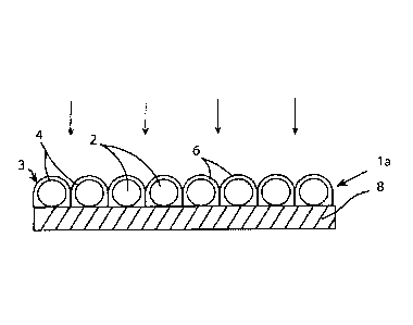
Figure 1 shows a schematic drawing of a light absorbing layer la according to
the invention. The light
absorbing layer la comprises a plurality of grains 2 made of a doped
semiconducting material, and an
electric charge conductor 3 in physical and electrical contact with the grains
2. A junction 4 is formed
in the contact area between the charge conductor 3 and the grains 2. The
grains 2 are partly covered
with the charge conductor 3 so that a plurality of junctions 4 are formed
between the grains and the
charge conductor. Preferably, at least 50% of the surface of the grains 2 is
covered with the charge
conductor.
The semiconducting material of the grains 2 has the ability to absorb photons,
which excite electrons
from a valence band to a conduction band and by that create electron-hole
pairs in the
semiconducting material. Suitably, the semiconducting material is silicon.
However, other
semiconducting material can also be used, such as CdTe, CIGS, CIS, GaAs, or
perovskite. Preferably,
the average size of the grains is between 1 1.1m and 300 gm, and typically,
the average size of the
grains 2 is between 20 gm and 100 ilm.
The charge conductor 3 is made of a solid material, i.e. not liquid, and can
be a hole conductor or an
electron conductor. If the grains are n-doped, the charge conductor 3
preferably is a hole conductor,
and if the grains are p-doped, the charge conductor 3 preferably is an
electron conductor. The charge
conductor 3 is made of a charge conducting material, for example, a doped
semiconducting material,
such as silicon, or an organic conducting material, such as a conducting
polymer. Several transparent,
conductive
CA 3022237 2022-01-21
CA 03022237 2018-10-25
WO 2018/021952 14 PCT/SE2017/050016
polymers with sufficient conductivity may be used for this purpose. An example
of a suitable
hole conducting polymer to be used in combination with silicon grains is poly
(3,4-
ethylenedioxythiophene) polystyrene sulfonate (PEDOT:PSS). PEDOT:PSS is a
polymer
mixture of two ionomers. Other examples of suitable material for the charge
conductor 3 are
polyaniline, P3HT and Spiro-OMeTAD. If a polymer conductor is used, the charge
conductor
comprises a plurality of particles made of a polymer or mixtures of polymers.
The particles of
the charge conductor partly cover the surface of the grains. The junctions 4
have the ability
to provide separation of the pairs of photo-excited electrons and holes.
Depending on the
materials of the grains and the charge conductor, the junctions are
homojunctions, such as
p-n-junctions, or heterojunctions.
The grains 2 are essentially evenly distributed in the light absorbing layer,
and the charge
conductor 3 is located on the grains and in the space between the grains. The
size and shape
of the grains 2 may vary. The light absorbing layer la is applied to a layer
8. For example, the
layer 8 is a conducting layer. The grains 2 are in physical as well as
electrical contact with the
layer 8. A lower portion of the grains may be protruding into the layer 8.
In the example shown in figure 3, the charge conductor 3 is an
organic.conductor. The
charge conductor is disposed on the surfaces of the grains 2 so that a
plurality of charge
conducting layers 6 is formed on the grains. Thus, the surface of each of the
grains 2 is partly
covered with a charge conducting layer 6. Preferably, the charge conducting
layers 6 have a
thickness between 10 nm and 200 nm. Typically, the charge conducting layers 6
have a
thickness between 50 nm and 100 nm. The charge conductor 3 is disposed between
the
grains so that the grains are bonded to each other by means of the organic
charge
conductor. Thus, the charge conductor increases the mechanical strength of the
light
absorbing layer. Each of the grains has an upper surface facing the incident
light and a lower
surface facing away from the incident light. In this embodiment, the upper
surface of the
grains is wholly or at least partly covered with the charge conductor 3, and
the lower surface
is free from charge conductor to enable electrical contact with a conducting
layer 8, which is
not a part of the light absorbing layer.
Figure 2 shows schematically a cross-section though a photovoltaic device 10
according to a
first embodiment of the invention. In this embodiment, the photovoltaic device
10 is a solar
cell. Figure 3 shows an enlarged view of a part of the photovoltaic device 10.
The
photovoltaic device 10 comprises the light absorbing layer la including the
grains 2 and the
charge conductor 3 as shown in figure 1, a first conducting layer 16 in
electrical contact with
the grains 2 of the light absorbing layer la, a second conducting layer 18
electrically coupled
to the charge conductor 3, and an insulating layer 20 disposed between the
first and second
conducting layers 16, 18, to electrically insulate the first and second
conducting layers. The
light absorbing layer la is positioned on a top side of the photovoltaic
device. The top side
should be facing the sun to allow the sunlight to hit the grains 2 and
generate photo-excited
CA 03022237 2018-10-25
WO 2018/021952 15 PCT/SE2017/050016
electrons. The first conducting layer 16 serves as a back contact that
extracts photo-
generated electrons from the light absorbing layer la. The light absorbing
layer la is
disposed on the first conducting layer. Thus, the distance the excited
electrons and/or holes
need to travel until they are collected is short. A first contact 12 is
electrically connected to
.. the first conducting layer 16, and a second contact 14 electrically
connected to the second
conducting layer 18. A load L is connected between the contacts 12, 14. The
first and second
conducting layers 16, 18 are suitably metal layers made of metal or metal
alloy, for example,
titanium, or aluminium or an alloy thereof.
The device 10 further comprises a plurality of charge conducting paths 22 of a
charge
conducting material disposed between the light absorbing layer la and the
second
conducting layer 18 to enable charges, i.e. holes or electrons, to travel from
the light
absorbing layer la to the second conducting layer 18. The conducting paths 22
are suitably,
but not necessarily, made of the same material as the charge conducting layers
6 on the
grains. In this embodiment, the charge conductor 3 forms the layers 6 on the
grains as well
as the conducting paths 22. The conducting paths 22 penetrate through the
first conducting
layer 16 and the insulating layer 20. Suitably, the first and second
conducting layers 16, 18,
and the insulating layer 20 are porous to allow the charge conductor to
penetrate through
the conducting layers and the insulating layer 20 to form the paths 22. The
charge conductor
3 can be accommodated in pores of the first and second conducting layers 16,
18, and in
pores of the insulating layer 20.
The insulating layer 20 may comprise a porous insulating substrate. For
example, the porous
insulating substrate is made of a glass microfiber or a ceramic microfiber.
The first
conducting layer 16 is disposed on an upper side of the porous insulating
substrate, and the
second conducting layer 18 is disposed on a lower side of the porous
insulating substrate.
The light absorbing layer la is disposed on the first conducting layer 16.
Figure 3 shows an enlarged part of the light absorbing layer la and the first
conducting layer
16. In this embodiment, the first conducting layer 16 comprises a plurality of
conducting
particles 24 made of a conducting material. The conducting particles 24 are
suitably metal
particles made of metal or metal alloy, for example, titanium or aluminium or
an alloy
thereof. The conductive particles 24 of the first conducting layer are in
physical and electrical
contact with each other. The grains 2 are in physical and electrical contact
with some of the
conducting particles 24 of the first conducting layer. Preferably, the grains
2 have a size less
than 100 p.m in order to provide a sufficient contact area between the grains
and the
particles 24 of first conducting layer 16. The grains 2 have an upper portion
facing away from
the photovoltaic device and a lower portion in physical contact with the
conducting particles
24 of the first conducting layer. The upper portions of the grains 2 are
covered with the
conducting layers 6 of the charge conductor 3.
The grains are preferably made of doped silicon, and a zone of physical
contact between the
silicon grains 2 and the conducting particles 24 of the first conducting layer
consists of a
=
CA 03022237 2018-10-25
W02018/021952 16 PCT/SE2017/050016
layer 26 of metal-silicon alloy or metal suicide in order to provide good
electrical contact
between the grains 2 and the particles 24. For example, the grains 2 are made
of silicon (Si)
and the conducting particles 24 are made of titanium (Ti), or at least partly
comprise
titanium, and the boundaries between the grains 2 and the particles 24
comprise a layer 26
of titanium suicide, which provides good electrical contact between Si and Ti.
Due to the fact that the first conducting layer 16 is formed by a plurality of
conducting
particles 24 bonded to each other, cavities are formed between the particles.
Thus, the first
conducting layer 16 allows the charge conductor 3 to extend through the first
conducting
layer to form the plurality of charge conducting paths 22. The charge
conductor 3 is
accommodated in some of the cavities formed between the conducting particles
24 in the
first conducting layer 16.
In order to avoid electrical contact between the first conducting layer 16 and
the conducting
paths 22 of the charge conductor 3, the conducting particles 24 are at least
partly covered
with an insulating layer 28 of an insulating material, for example, an
insulating oxide.
Preferably, the parts of the surfaces of the conducting particles 24, which
are not in contact
with the grains 2 or with the other conducting particles 24 in the layer, are
covered with the
insulating layer 28. The charge conducting paths 22 of the charge conductor 3
are in contact
with the insulating layers 28 on the particles 24, as shown in figure 3. A
layer of insulating
metal oxide is, for example, formed by oxidizing the conducting particles 24
during
manufacturing of the device 10. The insulating layer 28 of metal oxide
provides a protective
and electrically insulating layer on the particles, which prevents that
charges are transferred
between the first conducting layer 16 and the charge conductor 3, and thereby
prevents
short circuit between the first conducting layer 16 and the charge conductor
3. For example,
if the conducting particles comprise titanium, the parts of the surfaces of
the titan particles,
which are not in contact with the grains, are covered with titanium oxide
(1102). For
example, if the conducting particles comprise aluminium, the parts of the
surfaces of the
conducting particles, which are not in contact with the grains, are covered
with aluminium
oxide (Al2O3).
The second conducting layer 18 may also comprise conducting particles. The
conducting
particles of the second conducting layer 18 are suitably metal particles made
of metal or
metal alloy, for example, titanium, aluminium, or an alloy thereof. In this
example, the
conducting particles (not shown) of the second conducting layer 18 are made of
aluminium,
and the aluminium particles are not covered with any insulating layer, and
accordingly, the
charge conductor is allowed to be in electrical contact with the particles of
the second
conducting layer 18. The conducting particles of the conducting layers 16, 18
are sintered to
form the conducting layers. The conducting particles in each of the conducting
layers 16, 18
are in electrical contact with each other to form a conducting layer. However,
there is also
space between the conducting particles to accommodate the charge conductor 3.
The
junctions 4 on the grains 2 of the light absorbing layer are in electrical
contact with the paths
CA 03022237 2018-10-25
WO 2018/021952 17 PCT/SE2017/050016
22 of charge conducting material, which are in electrical contact with
conducting particles in
the second conducting layer 18.
Figure 4 shows schematically a cross-section though a part of a photovoltaic
device 30
according to a second embodiment of the invention. The photovoltaic device 30
is a solar
cell. In figure 4 the same and corresponding parts are designated by the same
reference
numerals as in figures 1 - 3. Figure 4 is a very simplified schematic view of
the architecture of
the device. In this example, the grains 2 are made of n-doped silicon, the
first and second
conducting layers include conducting particles 24, 25 made of titanium, and
the charge
conductor 3 is a hole conducting polymer. In this example the hole conducting
polymer is
PEDOT:PSS, in the following denoted PEDOT. PEDOT is a hole conductor and
transports holes
to the second conducting layer 18. The n-doped silicon grains are electron
conductors and
transport electrons to the first conducting layer. The first conducting layer
then transports
the electrons to the second conducting layer via an external electrical
circuit. The grains 2
are, for example, made of crystalline silicon. The silicon grains may have
predominantly
{1111 planes exposed at the surface. Instead of showing many silicon grains 2
and many
titanium conducting particles 24, 25, only two silicon grains 2 and two
titanium conducting
particles 24, 25 in each of the conducting layers 16, 18, are shown. It is to
be understood
that the real solar cell contains many thousands or even millions of grains 2
lying next to
each other in the light absorbing layer. But two particles is the minimum
number needed to
demonstrate the architecture and the working principle of the solar cell.
The photovoltaic device 30 comprises an insulating layer 20 in the form of a
porous
insulating substrate, a first conducting layer 16 disposed on one side the
insulating layer, a
second conducting layer 18 disposed on the opposite side of the insulating
layer, and a light
absorbing layer la disposed on the first conducting layer 16 and in electrical
contact with the
first conducting layer. The conducting layers 16, 18 are connected to an
external electric
load 32. The first and second conducting layers 16, 18 are separated
physically and
electrically by the insulating layer 20. A layer 26 of titanium silicide
(TiSi2) is formed between
the silicon grains 2 of the light absorbing layer la and the titanium
conducting particles 24 of
the first conducting layer 16. The silicon grains 2 of the light absorbing
layer la are bonded
to the titanium particles. The titanium conducting particles 24 in the first
conducting layer 16
are in physical and electrical contact with each other, and the titanium
conducting particles
25 in the second conducting layer 18 are in physical and electrical contact
with each other.
The titanium particles in the conducting layers 16, 18 are partly covered by
insulating layers
28 of insulating titanium oxide (h02). The parts of the surfaces of the
titanium conducting
particles 24, which are in contact with the grains 2 or with the other
conducting particles 24
in the layer, are not covered with titanium oxide. A zone 38 between the light
absorbing
layer la and the first conducting layer 16 comprises titanium oxide (TiO2) and
silicone oxide
=
CA 03022237 2018-10-25
WO 2018/021952 18
PCT/SE2017/050016
The photovoltaic device 30 differs from the photovoltaic device 10 shown on
figure 2 in that
it comprises a connection site 34 electrically coupled to the second
conducting layer 18 and
electrically insulated from the first conducting layer. The connection site 34
may comprise a
metal layer. In this example, the connection site 34 comprises a layer made of
silver (Ag). It is
suitable to use silver, since it provides good electrical contact both with
titanium and PEDOT.
Another advantage with using silver is that silver prevents formation of oxide
on the
titanium particles 25 of the second conducting layer 18 in the area of contact
between the
titanium particles and the connection site 34. Instead, a layer 36 of titanium
silver (AgTi) is
formed between the titanium particles 25 of the second conducting layer 18 and
the
connection site 34. Thus the PEDOT can form a good low ohmic contact with
silver and the
silver can form a good low ohmic contact with titanium via the AgTi.
Consequently, PEDOT
can contact the titanium indirectly via the silver and the AgTi. Other
materials may be used
in the connection site, for example, carbon based materials such as graphite
or amorphous
carbon.
The charge conductor 3 is arranged in physical and electrical contact with the
grains 2 of the
light absorbing layer la. The charge conductor 3 is also arranged in
electrical contact with
the connection site 34, which is electrically coupled to the second conducting
layer 18. In
this embodiment, the charge conductor 3 is electrically insulated from the
first and second
conducting layers 16, 18 by means of the insulating layers 28 on the
conducting particles 24,
25. The charge conductor 3 covers a main part of the grains 2, and extends
through the first
conducting layer 16, the insulating layer 20, and the second conducting layer
18, as shown in
figure 4. The charge conductor 3 is in contact with the oxide layers 28 on the
particles in the
first and second conducting layers. The charge conductor 3 is electrically
insulated from the
conducting particles 24, 25, and accordingly from the first and second
conducting layers by
means of the insulating oxide 28. The charge conductor 3 is in physical and
electrical contact
with the connection site 34. The charge conductor 3 is indirectly in physical
and electrical
contact with the titanium particles 25 via the connecting site 34. Thus, the
connecting site
serves the purpose of making sure that the charge conductor can transfer holes
to the
titanium particles 25 of the second conducting layer. The photovoltaic device
may also
comprise a casing or other means for enclosing the photovoltaic device.
In the following, there is a step by step explanation on how the solar cell
disclosed in figure 4
works:
Step 1. A photon creates an excited electron ¨ hole pair inside the grains 2.
In this example,
the charge conductor 3 is PEDOT, the grain 2 is made of silicon, and the
interface 40 is a
PEDOT¨silicon interface.
Step 2. The excited electron then travels through the grain 2 and across the
zone 26 of metal
silicon interface and enters into the conducting particle 24. In this example,
the particle 24 is
a Ti particle and the layer 26 comprises TiSi2. Thus, the electron passes the
Si ¨ TiSi2 ¨ Ti
CA 03022237 2018-10-25
WO 2018/021952 19 PCT/SE2017/050016
interface. The excited hole, on the other hand, travels across the interface
40 into the layer
of charge conductor 3.
Step 3. The electron in the conducting particle 24 can then be transferred to
neighbouring
particles 24 and then be collected in an external electric circuit via an
external electric load
32. In the meantime the hole travels inside the charge conducting paths 22 of
the charge
conductor 3 all the way down to the low ohmic silver layer of the connection
site 34.
Step 4. After passing the external electric load 32 the electron is
transferred to the second
conducting layer 18. The electron is then transferred to the Ti-TiAg-Ag layer
36. The hole in
the charge conductor 3 is transferred to the silver layer of the connection
site 34 and
lo recombines with the electron in the connection site 34.
Six crucial interfaces can be identified in the example disclosed in figure 4:
1. Charge conductor ¨ grain interface
The grains 2 must be essentially oxide free in order to achieve an efficient
charge separation
of electrons and holes at the interface 40 between the grains 2 and the charge
conductor 3
to enable generation of high photocurrent and high photo voltage. The
thickness of an oxide
layer on the grains should be only a few nanometres thick or even thinner for
obtaining
efficient charge separation. In this embodiment, the grains 2are made of doped
silicon, the
charge conductor 3 is made of PEDOT, and accordingly the interface 40 is a
PEDOT-Si
interface. The silicon must be essentially oxide free, i.e. no or very little
SiO2 on the Si
surface in order to achieve an efficient charge separation of electrons and
holes at the
PEDOT-Si interface.
2. Conducting particle ¨grains
A layer 26 of metal silicide is formed between the grains 2 and the conducting
particles 24 of
the first conducting layer. The metal silicide should be of sufficiently high
conductivity to
minimize resistive losses when electrons are transferred from the grains to
the conducting
particles. In this embodiment, the conducting particles are made of titanium
(Ti), and
accordingly the layer 26 between the silicon grains and the titanium particles
consists of
titanium silicide (TiSi2).
3. Charge conductor ¨ metal silicide ¨ oxide
To avoid short circuit, there should be an insulating layer 38 between the
charge conductor
3, the metal silicide layer 26, and the insulating oxide layer 28. In this
embodiment, the
insulating layer 38 consists of titanium oxide (TiO2) and silicon oxide
(SiO2). The TiO2-SiO2
layer 38 must be sufficiently thick to achieve good electrical insulation
between PEDOT and
TiSi2. If the TiO2-SiO2 layer 38 is too thin there will be short circuit
between PEDOT and TiSi2
with lowered photocurrent and photo voltage as consequence.
CA 03022237 2018-10-25
WO 2018/021952 20 PCT/SE2017/050016
4. Charge conductor ¨ conducting particles
In order to achieve insulation between the charge conductor 3 and the
conducting particles
24, 25 of the first and second conducting layers, the conducting particles is
covered with an
insulating oxide layer 28. In this embodiment, the insulating oxide layer 28
consists of
titanium oxide, such as TiO2. The titanium oxide layer 28 must be sufficiently
thick in order
to achieve sufficient electrical insulation between the PEDOT and the
titanium. If the
titanium oxide layer is too thin, the photo voltage and the photocurrent will
be lowered
because of short-circuit between PEDOT and titanium.
5. Connection site - conducting particles
Between the conducting particles 25 of the second conducting layer and the
connection site
34, there is a conducting a layer 36. In this embodiment, the conducting layer
36 consists of
titanium silver (TiAg). The conducting layer 36 must be thick enough to
provide a good low
ohmic electric contact between the conducting particles 25 of the second
conducting layer
and the connection site 34, e.g. between the silver (Ag) and the titanium
(Ti).
6. Connection site - charge conductor
The charge conductor 3 is in contact with the connection site 34 at an
interface 42. The
charge conductor 3, in this embodiment PEDOT, should cover the silver of
connection site 34
sufficiently to avoid resistive losses in order to achieve maximum
photocurrent.
In the following, an example of a method for manufacturing a photovoltaic
device according
to the invention will be described.
Step 1: Forming a first porous conducting layer on one side of a porous
insulating substrate.
This is, for example, done by printing with an ink including conductive
particles on one side
of the porous insulating substrate. The porous insulating substrate is, for
example, a porous
glass microfiber based substrate.
For example, a first ink is prepared by mixing 10 um sized TiH2 particles with
terpineol. The
ink comprises TiH2 particles with a diameter that is smaller than 10
micrometres.
Subsequently, the first ink is printed onto a porous glass microfiber based
substrate. The
printed layer will form a first porous conducting layer. Suitably, the
conductive particles are
too large to be able to penetrate through the porous insulating substrate.
Step 2: Forming a second porous conducting layer on an opposite side of the
porous
insulating substrate. This is, for example, done by printing with an ink
including conductive
particles on the opposite side of the porous insulating substrate. Suitably,
the conductive
particles are too large to be able to penetrate through the porous insulating
substrate.
For example, a second ink is prepared by mixing TiH2 with terpineol. The ink
comprises TiH2
particles with a diameter that is smaller than 10 micrometres. The filtered
ink is then mixed
CA 03022237 2018-10-25
WO 2018/021952 21 PCT/SE2017/050016
with silver plated conductive particles in order to make an ink for depositing
the second
conducting layer. Subsequently, the second ink is printed onto the opposite
side of the
porous insulating substrate. The second printed layer will form a second
conducting layer.
Step 3: Coating the first porous conducting layer with a layer of grains made
of a doped
semiconducting material to form a light absorbing layer. This is, for example,
done by
printing with an ink including a powder of grains of a doped semiconducting
material, such
as doped silicon, on the first conducting layer. Alternatively, powder of
grains of a doped
semiconducting material, such as doped silicon, can be sprayed on the first
conducting layer.
Suitable spraying techniques are, for example, electro spraying or
electrostatic spraying. The
silicon particles may be etched in a separate step before deposition on the
first conducting
layer. The etching of the silicon particles can be performed using, e.g.
isotropic etching
solutions or anisotropic etching solutions. The isotropic etching of the
silicon particles can be
used to remove impurities from the silicon surface. Anisotropic etching of the
silicon
particles can be used for a pyramid shaped etch pit where the pyramid shaped
silicon
surface can increase the effective light absorption by the silicon.
Step 4: Applying a pressure on the layer of grains so that portions of the
grains project into
the first porous conducting layer. For example, pressure can be applied on top
of the grains
by using a membrane press or by using a roller press. Step 4 is optional.
Step 5: Heat treating the solar cell under vacuum until the grains have been
sintered to the
first porous conducting layer. The layer of grains and the porous conducting
layers are
vacuum sintered to form a porous layer of grains on the first conducting
layer. During the
sintering, the grains bond to the conducting particles of the first conducting
layer to achieve
mechanical and electrical contact between them. Also, during vacuum sintering
the
conducting particles are sintered together to form a first conducting layer
with mechanical
and electrical contact between the conducting particles. Preferably, the
assembly of
substrate, first and second conducting layer and grains is heat treated in
vacuum with a
temperature above 550 C during at least two hours. For example, the printed
substrate is
vacuum sintered at 650 C and then allowed to cool down to room temperature.
The
pressure during sintering is lower than 0.0001 mbar. During the heat treating
in vacuum, the
silicon of the grains and the titanium of the particles are reacting and form
titanium silicide
in the boundaries between the grains and the particles. Thus, layers of
titanium silicide are
formed between the grains and the particles of the first conducting layer,
which improve the
electrical contact between the grains and the particles.
Step 6: Heat treating the solar cell in air until the available surface of
first porous conducting
layer has been oxidized. In a next step, the solar cell is heat treated in air
to achieve an
electrically insulating oxide layer on the conducting particles of the first
and second
.. conducting layer. The surface of the silicon particles becomes oxidized
during the heat
treatment in air.
CA 03022237 2018-10-25
WO 2018/021952 22 PCT/SE2017/050016
Step 7: Removing the silicon oxide layer on the silicon particles. In a next
step the silicon
oxide on the silicon particles is removed by treating the surface of the
silicon particles with
hydrogen fluoride. The surface of the silicon particles can be exposed to
hydrogen fluoride in
the form of a solution of HF in water. Alternatively the HF treatment of the
silicon particles
can be performed by exposing the surface of the silicon particles to gaseous
HF. The HF
treatment has the effect of removing silicon oxide from the surface of the
silicon particles.
Step 8: Deposition of PEDOT:PSS. In a next step PEDOT:PSS is deposited onto
the surface of
the silicon particles and inside pores of the first conducting layer and
inside the pores of the
insulating substrate and inside the pores of the second conducting layer. The
PEDOT:PSS can
be deposited from, e.g., a water based solution containing PEDOT:PSS. The
PEDOT:PSS
solution can be deposited by soaking the substrate with the first and second
conducing layer
and the silicon grains in a solution of PEDOT:PSS. Alternatively the PEDOT:PSS
deposition can
be performed in several steps. For example, the PEDOT:PSS solution can first
be sprayed
onto the silicon grains followed by drying off the solvent to yield a dry
solid PEDOT:PSS layer
on the surface of the silicon grains. In a second step the second conducting
layer is sprayed
with a solution of PEDOT:PSS A suitable spraying technique to achieve a thin
layer of
PEDOT:PSS on the silicon grains is, e.g., ultrasonic spraying.
The photovoltaic device according to the invention comprises grains of
semiconducting
particles and therefore manufacturing and handling of wafers or build-up of
thin films of
brittle material is avoided. The grains as such is a cheaper material and
easier to handle in an
industrial production. The grains can easily be applied by printing or similar
methods. A
possible defect on the surface of grains will only have local influence on the
efficiency of the
cell. Accordingly, this photovoltaic device is cheaper than the prior art
photovoltaic devices.
An environmentally friendly and stable material with high conversion
efficiency, such as
silicon, can be used as the grains in the light absorbing layer. The
photovoltaic device
according to the invention can be made thin and flexible.
Figure 5 shows an example of a light absorbing layer 1b according to a second
embodiment
of the invention. The light absorbing layer lb comprises a plurality of grains
2 made of a
semiconducting material of a first type of doping, and a charge conductor 3
comprising a
plurality of particles 52 made of a semiconducting material of a second type
of doping. The
average size of the semi-conducting particles 52 is smaller than the average
size of the grains
2 to allow the semi-conducting particles to be accommodated in spaces formed
between the
grains 2. For example, the average size of the grains 2 is less than 1 mm, and
the average size
of the semi-conducting particles 52 is preferably less than 0.1 mm to allow
them to
accommodate in the space formed between the grains 2.
Suitably, the semiconducting material of the grains 2 and the particles 52 is
silicon, and the
grains 2 and the particles 52 are made of silicon with different types of
doping. However,
other semiconducting material can also be used. For example, the grains 2 can
be made of
CdTe, CIGS, CIS or GaAs, and the semiconducting particles 52 can be made of
CuSCN or Cul.
=
CA 03022237 2018-10-25
WO 2018/021952 23
PCT/SE2017/050016
The grains 2 and the particles 52 are in physical and electrical contact with
each other so
that a plurality of junctions is formed in a contact area between them. The
type of the
doping of the grains 2 and the semiconducting particles 52 are such that the
junctions can
provide separation of photo-excited electrons and holes. Due to the different
types of
doping of the grains 2 and the semiconducting particles 52, a "depletion
region" is created in
the area where the grains 2 and the semiconducting particles 52 are in contact
with each
other. When the electron-hole pairs reach the "depletion region", the electron
and the hole
are separated. The first and second type of doping is, for example, of P-type
and N-type, and
by that the junctions are PN-junctions, or possible PIN-junctions.
Figure 6 shows schematically a cross-section though a photovoltaic device 50
according to a
third embodiment of the invention including the light absorbing layer lb
comprising the
grains 2 and the charge conductor 3, as shown in figure 5. The photovoltaic
device 50 further
comprises a first conducting layer 16 including conducting particles 24 in
electrical contact
with the grains 2, a second conducting layer 18 including conducting particles
25 electrically
coupled to the semiconducting particles 52 of the charge conductor 3, and an
insulating
layer 20 disposed between the first and second conducting layers. The
photovoltaic device
50 further comprises a first contact 12 electrically connected to the first
conducting layer
and a second contact 14 electrically connected to the second conducting layer.
The device 50 further comprises a plurality of charge conducting paths 22 of a
charge
conducting material disposed between the light absorbing layer lb and the
second
conducting layer 18. In this embodiment, the charge conducting paths 22
comprise a
plurality of semiconducting particles made of a charge conducting material.
For example, the
semiconducting particles in the paths 22 are made of doped silicon. Suitably,
the
semiconducting particles in the path are made of the same material as the
semiconducting
particles 52 in the light absorbing layer. The charge conductor 3 is deposited
in such a way
that some of the semi-conducting particles 52 partly cover the grains 2 and
some of the
semi-conducting particles 52 form a plurality of continuous paths 22 of charge
conducting
material from the surface of the grains 2 to the second conducting layer.
Suitably, the first
and second conducting layers, and the insulating layer 20 are porous to allow
the
semiconducting particles 52 of the charge conductor 3 to penetrate through the
conducting
layers and the insulating layer. The semi-conducting particles 52 of the
charge conductor 3
are accommodated in pores of the first and second conducting layers and in
pores of the
insulating layer 20, as shown in figure 6. The semi-conducting particles 52 of
the charge
conductor are in electrical contact with each other, and in electrical contact
with the grains 2
in the light absorbing layer so that at least some of the semi-conducting
particles 52 form a
semi-conducting network between the light absorbing layer lb and the second
conducting
layer.
The present invention is not limited to the embodiments disclosed but may be
varied and
modified within the scope of the following claims. For example, in an
alternative
=
CA 03022237 2018-10-25
WO 2018/021952 24
PCT/SE2017/050016
embodiment the grains can be embedded in the charge conductor. The
architecture of the
photovoltaic device may also vary. For example, the insulating layer and/or
the second
conducting layer can be omitted in other embodiments. The light absorbing
layer according
to the invention can also be used in a front contact photovoltaic device where
a metal anode
grid is positioned on top of the light absorbing layer, i.e. on the charge
conductor and the
grains. Additionally, the second conducting layer could be non-porous in the
form of a metal
film.