Note: Descriptions are shown in the official language in which they were submitted.
CA 03023069 2018-11-02
WO 2017/191459 PCT/GB2017/051249
Wireless Power Transfer System
This disclosure relates to wireless power transfer. In particular, this
disclosure relates to an
inverter based on the class-EF topology which is suitable for driving a
transmitter coil in an
inductive power transfer system.
Background
Wireless power transfer has many industrial applications, and devices
utilising wireless
power transfer, such as wireless toothbrush chargers, wireless charging pads
for mobile
devices, and wirelessly charged medical devices implanted within the body,
continue to grow
in popularity.
Inductive power transfer (IPT) is an example of non-radiative wireless power
transfer. In a
typical inductive power transfer system, an alternating current passes through
a transmitter
coil. This causes the transmitter coil to produce a time-varying magnetic
field. When a
receiver coil is placed in the time-varying magnetic field, the magnetic field
induces an
alternating current in the receiver coil, which can then be used to drive a
load. Thus, power
is transmitted wirelessly from the transmitter coil to the receiver coil
through the time-varying
magnetic field.
When designing an inductive power transfer system, several factors need to be
borne in
mind, and several problems present themselves. In order to achieve efficient
operation and
maximum power throughput, it is generally required to operate the IPT system
using a large
magnetic field. However, design of the system can be restricted in this
respect, for example
by guidelines relating to exposure limits for electromagnetic fields set by
the International
Commission on Non-lonising Radiation Protection (ICNI RP).
It is possible to use a power inverter to convert a DC signal to an AC signal
in order to drive
a transmitter coil in an IPT system. It is also possible to use a transistor
as a switch within
the inverter. When using a transistor switch however, two types of power loss
can present
themselves: conduction loss, and switching loss. The first is associated with
the finite
resistance of the transistor, whilst the second is associated with switching
the transistor at
non-zero voltage and non-zero current. This second type of power loss can be
minimised
using 'soft-switching' techniques, for example zero-voltage-switching (ZVS)
techniques. ZVS
involves switching the transistor on/off whilst zero voltage passes through
the transistor.
With the above in mind, a problem with existing systems is that the magnetic
field
transmitted by a transmitter coil is dependent on the receiver load. For
example, in a system
1
SUBSTITUTE SHEET (RULE 26)
8441029
with multiple devices each having a respective receiver load, the power
available to any one
device can be reduced if another receiver device moves closer to the
transmitter coil. Also,
introducing a new receiver device to the IPT system can reduce the power
available to all the
original receiver devices. The number, location, and orientation of the
receiver coils in the IPT
system affects the effective resistive load of the transmitter coil, which
brings about a change in
the current passing through the transmitter coil. This in turn alters the
magnetic field produced
by the transmitter coil. This variation in magnetic field may cause the
magnetic field to exceed
ICNIRP limits and/or cause an unwanted reduction in maximum achievable range
or power
throughput. The change in current also causes increased power losses, and
hence reduced
efficiency of the IPT system, due to loss of ZVS operation.
It is desirable to provide an inverter for driving a transmitter coil which
retains a high efficiency
and which delivers a constant current to the transmitter coil, independent of
the load. In
providing such an inverter, it is also desirable to avoid or reduce the
overhead of real-time
circuit and system level control. It is also desirable to avoid switching
losses which may occur
whilst the transistor is being turned on and off.
Summary
According to an aspect of the present invention, there is provided a power
inverter adapted to
drive a transmitter coil in an inductive power transfer system, wherein the
inverter is adapted to
class 'EF' operation, is arranged to drive a load resistance, and comprises: a
switching device
arranged between a power source and ground and arranged to switch at a
switching frequency;
and a resonant network arranged in parallel with the switching device between
the power source
and ground, the resonant network having a resonant frequency which is a non-
integer multiple of
the switching frequency, such that, in operation, an AC current having a
substantially constant
amplitude and phase passes through the load resistance regardless of
variations in the load
resistance; wherein the resonant network comprises a resonant circuit
comprising a resonant
circuit inductor and a resonant circuit capacitor.
According to another aspect of the present invention, there is provided a
method of fabricating a
power inverter adapted to drive a transmitter coil in an inductive power
transfer system, wherein
the inverter is adapted to class 'EF' operation, is arranged to drive a load
resistance, and the
method comprises: arranging a switching device between a power source and
ground; arranging
the switching device to switch at a switching frequency; arranging a resonant
network in parallel
with the switching device between the power source and ground; arranging the
resonant network
to have a resonant frequency which is a non-integer multiple of the switching
frequency, such
that, in operation, an AC current having a substantially constant amplitude
and phase passes
2
Date Recue/Date Received 2022-08-26
8441029
through the load resistance regardless of variations in the load resistance;
wherein the resonant
network comprises a resonant circuit comprising a resonant circuit inductor
and a resonant circuit
capacitor.
According to another aspect of the present invention, there is provided a
rectifier adapted to
receive an AC signal from a receiver coil in an inductive power transfer
system, wherein the
rectifier is adapted to class 'EF' operation, is arranged to drive a load
resistance, and comprises:
a switching device arranged between a power source and the load resistance and
arranged to
switch at a switching frequency; and a resonant network having a resonant
frequency which is a
non-integer multiple of the switching frequency and arranged such that, in
operation, an
AC current having a substantially constant amplitude and phase passes through
the load
resistance regardless of variations in the load resistance; wherein the
resonant network
comprises a resonant circuit comprising a resonant circuit inductor and a
resonant circuit
capacitor.
According to another aspect of the present invention, there is provided an
inductive power transfer
system comprising a transmitter circuit and a receiver circuit, the
transmitter circuit comprising:
the inverter described above; and the rectifier described above.
According to another aspect of the present invention, there is provided a
method of fabricating a
rectifier adapted to receive an AC signal from a receiver coil in an inductive
power transfer system,
wherein the rectifier is adapted to class 'EF' operation, is arranged to drive
a load resistance, the
method comprising: arranging a switching device between a power source and the
load
resistance; arranging the switching device to switch at a switching frequency;
and arranging a
resonant network having a resonant frequency which is a non-integer multiple
of the switching
frequency, such that, in operation, an AC current having a substantially
constant amplitude and
phase passes through the load resistance regardless of variations in the load
resistance; wherein
the resonant network comprises a resonant circuit comprising a resonant
circuit inductor and a
resonant circuit capacitor.
According to another aspect, there is provided a power inverter for driving a
transmitter coil in
an inductive power transfer system, wherein the inverter is suitable for class
'EF' operation. The
power inverter is arranged to drive a load resistance. The power inverter
comprises a switching
device arranged between a power source and ground and arranged to switch at a
switching
frequency, and a resonant network arranged in parallel with the switching
device between the
power source and ground. The resonant network has a resonant frequency which
is a non-integer
2a
Date Recue/Date Received 2022-08-26
8441029
multiple of the switching frequency, such that, in operation, a substantially
constant current
passes through the load resistance.
According to another aspect, there is provided a power inverter for driving a
transmitter coil in an
inductive power transfer system, wherein the inverter is suitable for class
'E' operation. The
power inverter is arranged to drive a load resistance. The power inverter
comprises a switching
device arranged between a power source and ground and arranged to switch at a
switching
frequency, and a resonant network arranged in parallel with the switching
device between the
power source and ground. The resonant network has a resonant frequency
2b
Date Recue/Date Received 2022-08-26
CA 03023069 2018-11-02
WO 2017/191459
PCT/GB2017/051249
which is a non-integer multiple of the switching frequency, such that, in
operation, a
substantially constant current passes through the load resistance.
It will be appreciated that the ground could alternatively be a reference node
other than
ground.
Optionally, in some embodiments, a first node of the switching device is
coupled to ground, a
second node of the switching device is coupled via a first inductor to a DC
supply voltage,
and a third node of the switching device is used to switch the switching
device on and off.
Optionally, in some embodiments, a first capacitor is coupled in parallel with
the switching
device between the power source and ground.
Optionally, in some embodiments, the resonant network comprises a resonant
circuit, the
resonant circuit comprising a second inductor and a second capacitor.
Optionally, in some embodiments, the load comprises the resistance of a
transmitter coil.
Optionally, in some embodiments, the load resistance comprises the resistance
of at least
one receiver coil.
Optionally, in some embodiments, the value of the load resistance can vary.
Optionally, in some embodiments, the non-integer multiple is preferably
between 1 and 2, is
more preferably between 1.5 and 1.65, and is even more preferably equal to 1.5
Optionally, in some embodiments, a third capacitor and a third inductor are
coupled in series
with the load resistance.
Optionally, in some embodiments, the inverter is arranged to maintain zero-
voltage-switching
operation.
According to another aspect, a method of fabricating a power inverter for
driving a
transmitter coil in an inductive power transfer system is provided. The
inverter is suitable for
class `EF' operation, is arranged to drive a load resistance, and the method
comprises
arranging a switching device between a power source and ground, and arranging
the
switching device to switch at a switching frequency. The method also comprises
arranging a
resonant network in parallel with the switching device between the power
source and
ground. The method also comprises arranging the resonant network to have a
resonant
frequency which is a non-integer multiple of the switching frequency, such
that, in operation,
a substantially constant current passes through the load resistance.
3
SUBSTITUTE SHEET (RULE 26)
CA 03023069 2018-11-02
WO 2017/191459
PCT/GB2017/051249
According to another aspect, a method of fabricating a power inverter for
driving a
transmitter coil in an inductive power transfer system is provided. The
inverter is suitable for
class 'E' operation, is arranged to drive a load resistance, and the method
comprises
arranging a switching device between a power source and ground, and arranging
the
switching device to switch at a switching frequency. The method also comprises
arranging a
resonant network in parallel with the switching device between the power
source and
ground. The method also comprises arranging the resonant network to have a
resonant
frequency which is a non-integer multiple of the switching frequency, such
that, in operation,
a substantially constant current passes through the load resistance.
.. Optionally, in some embodiments, the inverter is as described above in
relation to the first
aspect.
According to an aspect, a rectifier for receiving an AC signal from a receiver
coil in an
inductive power transfer system is provided, wherein the rectifier is suitable
for class rEF'
operation and is arranged to drive a load resistance. The rectifier comprises
a switching
device arranged between a power source and the load resistance and arranged to
switch at
a switching frequency, and a resonant network having a resonant frequency
which is a non-
integer multiple of the switching frequency and arranged such that, in
operation, a
substantially constant current passes through the load resistance.
According to another a rectifier for receiving an AC signal from a receiver
coil in an inductive
power transfer system is provided, wherein the rectifier is suitable for class
'E' operation and
is arranged to drive a load resistance. The rectifier comprises a switching
device arranged
between a power source and the load resistance and arranged to switch at a
switching
frequency, and a resonant network having a resonant frequency which is a non-
integer
multiple of the switching frequency and arranged such that, in operation, a
substantially
constant current passes through the load resistance.
Optionally, in some embodiments the non-integer multiple is preferably between
1 and 2, is
more preferably between 1.5 and 1.65, and is even more preferably equal to
1.5.
Optionally, in some embodiments the power source comprises a receiver coil.
According to another aspect, an inductive power transfer system comprising a
transmitter
circuit and a receiver circuit, the transmitter circuit comprising the
inverter as described
above and the receiver circuit comprising the rectifier as described above.
4
SUBSTITUTE SHEET (RULE 26)
CA 03023069 2018-11-02
WO 2017/191459
PCT/GB2017/051249
Optionally, in some embodiments the respective non-integer multiples of the
switching
frequencies of the inverter and rectifier are equal.
Optionally, in some embodiments the rectifier power source comprises a
receiver coil, the
inverter resistance load comprises a transmitter coil, wherein the transmitter
coil is spaced
from the receiver coil, and the receiver coil is arranged to receive power via
inductive power
transfer from the transmitter coil.
According to another aspect, a method of fabricating a rectifier for receiving
an AC signal
from a receiver coil in an inductive power transfer system is provided. The
rectifier is suitable
for class `EF' operation and is arranged to drive a load resistance. The
method comprises
arranging a switching device between a power source and the load resistance,
arranging the
switching device to switch at a switching frequency, and arranging a resonant
network
having a resonant frequency which is a non-integer multiple of the switching
frequency, such
that, in operation, a substantially constant current passes through the load
resistance.
According to another aspect, a method of fabricating a rectifier for receiving
an AC signal
from a receiver coil in an inductive power transfer system is provided. The
rectifier is suitable
for class E' operation and is arranged to drive a load resistance. The method
comprises
arranging a switching device between a power source and the load resistance,
arranging the
switching device to switch at a switching frequency, and arranging a resonant
network
having a resonant frequency which is a non-integer multiple of the switching
frequency, such
that, in operation, a substantially constant current passes through the load
resistance.
Optionally, in some embodiments, the inverter is as described above.
Figures
Specific embodiments are now described with reference to the drawings, in
which:
Figure 1 is a schematic circuit diagram of a class EF inverter according to an
embodiment of
the present disclosure.
Figure 2 shows voltage and current waveforms for an inverter in accordance
with an
embodiment of the present disclosure.
Figure 3 shows voltage and current waveforms for an inverter in accordance
with an
embodiment of the present disclosure.
5
SUBSTITUTE SHEET (RULE 26)
CA 03023069 2018-11-02
WO 2017/191459
PCT/GB2017/051249
Figure 4 shows experimentally obtained voltage and current waveforms for an
inverter in
accordance with an embodiment of the present disclosure.
Figure 5 shows a class EF rectifier in accordance with an embodiment of the
present
disclosure.
Figure 6 shows three tables containing experimental results from three
different circuit
designs. Each table shows shunt capacitance, output current, and power-output
capability
for selected values of ql and p at 30% duty cycle operation.
Overview
Resonant soft-switching converters, such as Class E and Class EF2 inverters,
can be used
in high power wireless inductive power transfer (IPT) systems that operate at
multi-
megahertz frequencies due to their efficient operation and simple
construction. However,
resonant soft-switching converters are currently only optimised to operate at
optimum
switching conditions for a fixed load, and therefore are highly dependent on
the load value.
Current systems are therefore not tolerant to load variations, which causes
them to become
less efficient as the load deviates from its optimum value. Consequently, this
limits an IPT
system to function efficiently only at a fixed coil separation distance and
for a narrow load
range.
It is desirable for IPT systems to maintain high efficiency even with
significant variation in
receiver load and/or coupling factor between transmit and receive coils.
Variations in
coupling factor can be caused by relative motion between transmitter and
receiver coils, and
changes in receiver load can be caused by a change in power demand. In both
cases, the
resistive load which is reflected to the transmit coil from the receiver
changes. This has two
consequences. Firstly, efficiency of the transmit side class E (or related)
inverter may be
reduced due to loss of zero voltage switching (ZVS). Secondly, as the
resistive load of the
system changes, the transmit coil current can be changed, which in turn
changes the
magnetic field generated by the transmitter coil.
Disclosed herein is a load-independent Class EF inverter that maintains ZVS
operation, and
which produces a constant output current, rather than a constant output
voltage, regardless
of the load resistance. A constant output current allows the disclosed
inverter to operate
efficiently for a load range from zero resistance (short circuit) to a certain
maximum load
resistance, making the inverter more suitable as a coil driver for an IPT
system.
6
SUBSTITUTE SHEET (RULE 26)
CA 03023069 2018-11-02
WO 2017/191459
PCT/GB2017/051249
As would be understood, the parasitics of the class-E circuit, for example the
finite
resistance of the transistor, give rise to second harmonic currents. To
address this problem,
class-EF circuits may incorporate a resonant circuit, sometimes called a tank
circuit, which is
always tuned to an integer multiple of the switching frequency in order to
filter out the
corresponding harmonic signal. The circuit designer can use resonant circuits
to tune out
harmonics, such as the second and/or third harmonic. For example, if the
circuit designer
desires to filter out the second harmonic current, the resonant circuit is
designed to have a
resonant frequency which is twice the switching frequency in order to maximise
the
impedance faced by the second harmonic current.
In inverters according to the present disclosure, the resonant frequency of
the resonant
circuit is instead tuned to a non-integer multiple of the switching frequency.
This is
completely counter to the teaching of the current state of the art in Class-EF
based inverters,
and yet has the surprising effect that the current through the load is kept
constant. Constant
current operation means that the magnetic field is not subject to variations,
and thus the
magnetic field of the circuit can be kept in accordance with ICNIRP
guidelines. Also, ZVS
operation can be maintained, reducing switching losses in the inverter
transistor.
Detailed Description
The present invention will now be described more fully, and with reference to
the
accompanying drawings.
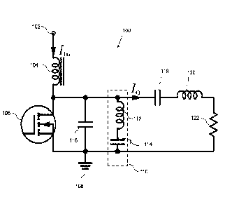
Figure 1 is a schematic circuit diagram of an inverter 100 according to the
present
disclosure. The inverter 100 is based on a class E inverter, and more
particularly is based on
a class `EF' inverter. In operation, the inverter 100 converts direct current
(DC) from a power
source 102 to alternating current (AC).
Class EF and Class E/F inverters are hybrid inverters that combine the
improved switch
voltage and current waveforms of Class F and Class F1 inverters with the
efficient switching
of Class E inverters. As a result, their efficiency, output power and power
output capability
can be higher in some cases than the Class E inverter.
The Class EF inverter is formed by adding a resonant network either in
parallel or series to
its load network. The method of adding resonant networks to the load network
is used in
Class F and ClassF1 inverters, and applying it to the Class E inverter results
in a hybrid
inverter, which has been referred to as the Class EF, or Class E/F, inverter.
The subscript n
refers to the ratio of the resonant frequency of the added resonant network to
the switching
frequency of the inverter and is always an integer number greater than or
equal to 2 in the
7
SUBSTITUTE SHEET (RULE 26)
CA 03023069 2018-11-02
WO 2017/191459
PCT/GB2017/051249
current state of the art. The current convention is to use the "EF" term if n
is an even integer
and to use the "E/Fn" term if n is an odd integer. The added resonant network
or networks
could be in the form of a series LC lumped network that is connected in
parallel with the load
network.
As will be appreciated from the description below, the Class EF inverters and
rectifiers of the
present disclosure do not fit into the current naming convention, however they
are suitable
for Class EF operation because the current and voltage waveforms are shaped
using the
technique of an additional tuned LC network.
The inverter 100 incorporates a transistor 106. The transistor 106 may be a
metal¨oxide-
semiconductor field-effect transistor 106 (MOSFET) as is known in the art.
Figure 1 shows
an n-channel MOSFET. The transistor 106 is coupled to a first inductor 104
having a first
inductance L1. The first inductor 104 is coupled to the transistor 106 via a
first transistor
node, which, in the case that the transistor 106 is an N-channel MOSFET as in
Figure 1, will
be the 'drive' node. The first inductor 104 is in turn coupled to a power
source 102, which is
arranged to provide a DC input signal to the inverter 100. The transistor 106
is also coupled
to ground 108 via a second node which, in the case that the transistor 106 is
an n-channel
MOSFET, will be the 'source' node. Finally, the transistor 106 is switched on
/ off via a third
transistor node which, in the case that the transistor 106 is an n-channel
MOSFET, will be
the 'gate' node. The transistor 106 can be switched on/off by applying an
input from, for
example, a signal generator (not shown). Typically, the signal generator
produces a square
wave input signal.
A first capacitor 116 having a first capacitance C1 is connected in parallel
with the transistor
106, between the first inductor 104 and ground 108. It will be appreciated
that capacitor C1
allows the inverter 106 to operate in a ZVS mode. The voltage on C1 naturally
falls to zero
twice per cycle and these two events are the point where the transistor
changes state.
Thus, it is the function of the complete circuit (all the components operating
together) that
gives rise to these zero volt instances. The existence of the capacitor Cl
means there is a
finite rate of change of voltage across the transistor giving a finite time
for it to change state.
A resonant circuit 110 is also connected in parallel between the first
inductor 104 and ground
108. The resonant circuit 110 has a second inductor 112 having an inductance
L2, and a
second capacitor 114 having a second capacitance C2. The resonant circuit 110
has a
resonant frequency FT, which is dependent on the values of C2 and L2 as will
be appreciated
by those skilled in the art.
8
SUBSTITUTE SHEET (RULE 26)
CA 03023069 2018-11-02
WO 2017/191459
PCT/GB2017/051249
In embodiments of the present disclosure, the resonant circuit 110 is designed
to have a
resonant frequency Ft which is a non-integer multiple of the transistor 106
switching
frequency Fsw. Preferably, the non-integer multiple is between 1 and 2, is
more preferably
between 1.5 and 1.65, and is even more preferably equal to 1.5.
A third capacitor 118 having a third capacitance C3, a third inductor 118
having a third
inductance L3, and a transmitter coil (not shown) are also connected in
parallel with the
transistor 106 and the first capacitor 116. The resistance of the transmitting
coil forms part of
the resistive load 122 of the inverter 100. In operation, the resistive load
122 of the inverter
100 is also increased in accordance with the respective resistive loads of any
receiver coils
within the IPT system. These respective receiver loads are 'reflected' to the
transmitter coil
when the IPT system is in operation, as will be understood by the skilled
person. The value
of the load may depend on the turns ratio and coupling factor, and can be
considered to
include the loss resistance of the receiver coil. It will thus be understood
that the resistive
load 122 experienced by the inverter 100 can vary as the receiver coils change
in number,
orientation, size or distance from the transmitter coil.
In the circuit of figure 1, lin is the steady input current. A significant DC
component with little
current ripple is expected. In is the sinusoidal output current that flows in
the transmit coil.
In operation, the power source 102 supplies a DC input signal to the inverter.
The transistor
106 is switched on and off at a switching frequency Fsw. This has the effect
of producing an
AC output signal, which passes through the load. As the AC current passes
through the
transmitter coil, a time-varying magnetic field is produced.
As will be appreciated by those skilled in the art, switching the transistor
106 on or off whilst
a non-zero current or voltage is passing through the transistor 106 gives rise
to switching
losses through the transistor 106, in accordance with the well-known equation
P=IV; where
P is the loss of energy in the transistor 106 per second, I is the current
passing through the
transistor 106 and V is the voltage across the transistor 106.
The resonant circuit 110, which has a resonant frequency which is a non-
integer multiple of
the switching frequency, acts to keep the current flowing through the
transmitter coil
constant, as will be described in more detail below.
Let the ratio of the resonant frequency Ft of the tuning circuit to the
switching frequency
be represented by parameter qt.
The current ly is sinusoidal and is given by equation (1):
:6011 ................................. sittfia
:0*
SUBSTITUTE SHEET (RULE 26)
CA 03023069 2018-11-02
WO 2017/191459
PCT/GB2017/051249
where I, is the output current's magnitude and (1) is its phase. It is assumed
that switch is
on for the period 0 < wt < 21-rD and off for the period 2nD < wt < 217.
Beginning with the
series tuning circuit network, its curr ent is given by equation (2):
where (3), (4), (5):
is;
...1, 4004 A.2.::!PONVItegtY=':04::::$ittl(4440r1
gitipt 4,0) +
-
......................................... f4.4
______________________________________________ q
L*C., ( =
4-041.1 Asti :k+
and the coefficients A2 and B2 are to be determined based on the equation's
boundary
conditions. The boundary conditions are determined from the current and
voltage continuity
conditions when the switch turns on and off. Parameter p is referred to as the
loading
parameter. The current in capacitor C1 is given by equation (6):
. .
.
:(0.5)
The drain for the period 2nD < wt < 2Tr is given by equation (7):
0.10#64.4) :ONO
V.
. õ.
where (8):
10
SUBSTITUTE SHEET (RULE 26)
CA 03023069 2018-11-02
WO 2017/191459
PCT/GB2017/051249
!]i.:.:.:it.t.: .1bi.. ' ' '
060:=:: ' ,: , __ . ' Olitht
- :
.,,I=VP, : V.':
and (9):
2431-.
::=:17 ,.. .,,, .
;tr::::: ,. ,,, :At.õ..,,,,4a.,,,t.,..1::
(9).
: ... . ,w,t1,4497
The voltage across the load resistor and the residual impedance in the output
load network
is given by equations (10), (11):
.:..,'. 0440:44(44:*:::4.)4,4 .'¨'
4.4* i:21 r**. : .
' .H ........................ 11(iiit);i004.(44+,0144*. :41.0!,,:
i
fill:
:ir* oi,::::=:.õ410.0; ' ' f,'.*: :
In the graph of Figure 2(a), the y axis shows \fps I W. The y axis is measured
in increments
of 1 from -Ito 3. The x axis shows wt, measured between 0 and 27T.
In the graph of Figure 2(b), the y axis shows lo / lin. The y axis is measured
in increments of
1 from 0 to 4. The x axis shows wt, measured between 0 and 2a.
.. In the graph of Figure 2(c), the y axis shows IDs / lin. The y axis is
measured in increments of
2 from -4 to 4. The x axis shows wt, measured between 0 and 2.rr.
In each of figures 2 (a), (b), and (c), a black line represents the optimum
resistance R0pt, a
grey line represents 0.75 Roll, and a blue / teal line shows 1.25 Ropt.
Figure 2 shows the effect of the load resistance varying by 25 % above and
below the
optimum load for a Class EF inverter. The graphs show the effect on the switch
voltage and
current and the output voltage for a Class EF inverter at a fixed duty cycle
of 37:5 %, q1 = 2
& k = 0:867
It can be noticed that ZVS is lost once the load varies above or below its
optimum value. For
higher load resistances the switch turns at a positive voltage which
discharges the charge in
capacitor C1 which results in a large current spike to flow through the
switch. In practice, the
11
SUBSTITUTE SHEET (RULE 26)
CA 03023069 2018-11-02
WO 2017/191459
PCT/GB2017/051249
current spike results in energy being lost in the switch's on resistance which
then degrades
the overall efficiency. It can also cause damage to the switch if its value
exceeds the switch's
current rating. The same occurs when the load resistance is below its optimum
value.
However, since a MOSFET with body diode may be used in the circuit, the body
diode
begins to conduct once the MOSFET's drain to source voltage crosses zero volts
and
exceeds the diode's forward. The current spike has a much lower magnitude here
since the
diode's forward voltage is low. Nevertheless, the overall efficiency will
still degrade.
Furthermore, the output current and voltage across the load resistance RL will
change as
the value of the load resistance changes.
To achieve load-independent operation, the following criteria are to be met
regardless of the
load value:
1. Constant output AC current
Equation 10 can be written in the form of equation (12), below:
I I! - ni:
' .. t(p) :: -::::!- .;,4, ;221, ::: (1121t
itlfri ''.:: ' !:.." ' Vil ¨ 44. Ai**
Since it has been assumed that there are no losses in the circuit, all the
power supplied by
the input voltage is consumed in the load. The following equation(13), can be
obtained
fiti 2b
(0)
(
Substituting the above equation, (13), in equation (12), gives equation (14):
Oi (P)::
Vt.: t14
= ,:ii
At4-4:: 1
.:õ
The loading parameter p would increase as the load resistance decreases and
vice versa. Thus p can
always be a positive real number, hence p C ik + . Referring to equation 14,
achieving a constant
12
SUBSTITUTE SHEET (RULE 26)
CA 03023069 2018-11-02
WO 2017/191459
PCT/GB2017/051249
output current against any load variations means the parameters of the
circuit, mainly the phase will
be constant for any value of p (i.e. independent of p) . This criteria means
that the rate of change of
0 f.A.0 , :. .
)
--.-----1-------'== ':!"';#. a' :000110*. (tli)
- :
equation 14 with respect to p will be zero, this can be represented by
equation (15):
2. Constant switching at zero-voltage
Zero-voltage switching or 'high efficiency' operation can be achieved by
setting the switch
voltage in equation 7 to zero, which produces the following, equation (16):
.:
3(2r) =0 0 bledt tio;:;i.: tior
4 '. ..: '
In the graph of Figure 3(a), the y axis shows \fps / V. The y axis is measured
in increments
of 1 from 0 to 3. The x axis shows wt, measured between 0 and 2-rr.
In the graph of Figure 3(b), the y axis shows X, (l0/V1). The y axis is
measured in
increments of 2 from -4 to 4. The x axis shows wt, measured between 0 and 2-
rr.
In the graph of Figure 3(c), the y axis shows X, (10/Vin). The y axis is
measured in increments
of 1 from 0 to 4. The x axis shows wt, measured between 0 and 2Tr.
In each of figures 3 (a), (b), and (c), a black line represents the nominal
load value R õm , a
grey line represents 00, and a blue / teal line shows 2 Rflom.
Figure 3 shows the voltage and current waveforms of the Class EF inverter at
different load
resistance values. In the graph of Figure 3, voltage and current waveforms are
shown for a
load independent Class EF inverter under various loads at fixed duty cycle of
30:0 %, q1 =
1:67 & k = 1:33. It can be seen that constant output current and ZVS are
maintained as the
load varies from its nominal value (Rnorn).
The output current for a desired p and load resistance is given by equation
(17):
__________________________________________________ =
(11):
0:itin 1: :: 14
13
SUBSTITUTE SHEET (RULE 26)
CA 03023069 2018-11-02
WO 2017/191459
PCT/GB2017/051249
The value of capacitor C1 is given by equation (18):
4.10
11)
:140:RIA ALA
For a given design the value of reactance Xwill also be fixed and independent
of the load.
Therefore function 1p2 can only be dependent on q, k, 0 and D. As a result,
the reactance X
normalised to cuCi for given solution set of q, k, 0 and D is given by
equation (19):
AgA trp(k..4: . Further to the above, as an
example, a load-independent Class EF inverter may be designed
to generate a constant output current with an amplitude of 5 A at 6.78 MHz for
a inductive
wireless power transfer system. The load resistance varies from a maximum 20
to a
minimum 0 0 and the coil inductance is 1:5 H.
In designing a suitable system, a circuit designer may begin by choosing
values for q1 and the
duty cycle. The following values and calculations serve as an example
embodiment of the
present disclosure.
As an example, it has been found that a q1 value of 1.5 and a duty cycle value
of 0.32 result
in operation at a high power-output capability and low variation in the drain
waveform. Next, a
designer may choose the input DC voltage. The input voltage may be chosen at
the point
where the output-capacitance of the switching device begins to reach a steady
value. The
switching device chosen may be, for example, the SiS888 MOSFET (150 V) from
Vishay. An
input DC voltage of 40V, for example, is suitable.
Next, a circuit designer may use equation (17) to find the value of the
loading factor p by
substituting the required output current value, the input DC voltage and the
maximum load
resistance. Using the above values, the value of p is 5:25 and consequently
the value of
parameter k is 0:656. From equation (18), the value of capacitor C1 is 635 pF.
Using the
obtained value of k, we find the value of capacitor C2 is 968 pF and
consequently the value of
inductor L2 is 252:9 nH. The resonant circuit can then be designed
accordingly.
14
SUBSTITUTE SHEET (RULE 26)
CA 03023069 2018-11-02
WO 2017/191459
PCT/GB2017/051249
From equation (19), a circuit designer using the above values would find the
value of the
residual reactance Xis 203 nH. Subtracting this value from the given coil
inductance gives an
inductance value of 1:3 pH. Capacitor C3 resonates with this inductance value
at the
switching frequency, consequently the value of capacitor C3 is 424 pF. The
circuit designer
now has all the component values, and can implement a load-independent Class
EF inverter
in accordance with the present disclosure.
Figure 4 shows experimentally obtained voltage and current waveforms for a
class EF
inverter having the above-described components. It can be seen that near ZVS
and constant
output current is maintained across the load resistance range.
In the graph of Figure 4(a), the y axis shows VDs(V). The y axis is measured
in increments of
from 0 to 120. The x axis shows wt, measured between 0 and 2-rr.
In the graph of Figure 4(b), the y axis shows X, (10/V1n). The y axis is
measured in increments
of 0.25 from -5 to . The x axis shows wt, measured between 0 and 2-rr.
In each of figures 4 (a) and (b), a black line represents 00, a grey line
represents 10, and a
15 blue / teal line shows 20.
It will be appreciated that an inverter according to the present disclosure
modifies the existing
class EF topology in a way which has never been done before to provide a
constant amplitude
output ac current along with maintaining zero voltage switching over a load
range from zero
resistance to an upper limit determined by the designer.
20 Existing class EF inverters may combine the class E topology with an (or
multiple) additional LC
network(s), which are always tuned to resonate at some harmonic (usually the
second and/or
third) of the switching frequency to reduce the harmonic content of the
voltage and/or current.
This is done to achieve some desired advantage over the pure class E topology
such as a
lower peak voltage across the switch. This additional LC network acts as a
harmonic filter and
is based on the traditional approach used in class F RF amplifiers. Current
approaches have
been based on the understanding that the only solutions to the sets of
equations describing
simultaneous load-independent output current and load-independent efficiency
are impractical.
In inverters according to the present disclosure, in contrast, rather than
tuning the resonant
circuit / additional LC network to resonate at a harmonic of the switching
frequency, the
resonant circuit is tuned to have a resonant frequency which is a non-integer
multiple of the
switching frequency. This enables the inverter to achieve desirable properties
such as constant
output current over variable load, which had hitherto been considered
impossible for the class E
SUBSTITUTE SHEET (RULE 26)
CA 03023069 2018-11-02
WO 2017/191459
PCT/GB2017/051249
based inverters. Tuning the additional LC tank to about 1.5 times the
switching frequency and
selecting the appropriate capacitance ratio, k=C1/C2, referring to equation
(3), both constant
current operation and maintenance of zero voltage switching over a wide
variation in load can
be achieved. k is typically selected to be greater than zero and less than
one, and more
preferably to be between 0.6 and 0.7.
Power inverters and rectifiers disclosed herein have resonant networks which
have a resonant
frequency which is a non-integer multiple of the switching frequency. The non-
integer multiple
is preferably between 1 and 2, is more preferably between 1.5 and 1.65, and is
even more
preferably equal to 1.5. There are also certain specific values of the integer
multiple within the
range 1 to 2 which give rise to particularly advantageous characteristics,
dependent on the
characteristics required from the inverter and/or rectifier. Circuits which
display these
advantageous characteristics are described below, with reference to the
experimental results
shown in the tables of figure 6. The circuits described can incorporate an
inverter and/or a
rectifier, and the characteristics described can be achieved in both an
inverter circuit and a
rectifier circuit.
It has been found that, if maximum power throughput operation is desired, a
non-integer
multiple of 1.58 is an optimal circuit design. In other words, this is the
design which gives the
highest power output from the inverter and/or rectifier at reduced voltage and
current stresses.
Maximum power throughput can be defined as the maximum product of output power
and
power-output capability. Experimental results for this 'max throughput'
circuit are shown in the
left-most table of figure 6 with varying values of the loading parameter, as
defined by equation
(5) above.
It has been found that, if maximum power-output capability is desired, a non-
integer multiple of
1.66 is an optimal circuit design. This design gives very low current and
voltage stresses.
Experimental results for this 'max cp' circuit are shown in the middle table
of figure 6 with
varying values of the loading parameter, as defined by equation (5) above.
It has been found that, if high switching frequency operation is desired, a
non-integer multiple of
1.69 is an optimal circuit design. This circuit design gives the highest
switching frequency
allowed by the transistors of the circuit. Experimental results for this 'max
frequency' circuit are
shown in the right-most table of figure 6 with varying values of the loading
parameter, as
defined by equation (5) above.
16
SUBSTITUTE SHEET (RULE 26)
CA 03023069 2018-11-02
WO 2017/191459
PCT/GB2017/051249
There are three key application scenarios in wireless power in which an
inverter according to
the present disclosure may be of benefit. These application scenarios are
given below as
examples.
1. Long range IPT. This scenario entails a single large transmit coil powering
a number of
mobile devices such as wireless sensor nodes in a large room at distances of,
for
example, up to around 10m. In order to achieve the maximum range it is
important for
the transmit coil to generate the highest permissible magnetic field within
ICNIRP limits.
This magnetic field stays constant independent of the number or location of
receiver
devices and will not be affected by changes in the local environment. For
example the
power available to one device is not reduced because another device has moved
closer
to the transmit coil. The present inverter enables this without additional
control
overhead. Furthermore power throughput control can be achieved simply by
receiver
load variation without affecting the operation of the transmitter.
2. Mid-range MHz IPT. This scenario entails high Q coils coupled weakly. The
transmitted
magnetic field can be kept constant as the receive coil moves further from the
transmit
coil, again enabling the range to be maximised without addition control to
prevent
exceeding the ICNIRP limits. Power throughput control can again be achieved
simply by
receiver load variation (at the expense of some link efficiency).
3. Short range IPT. In a closely coupled system the magnetic field strength is
strongly
determined by both coils and therefore simply controlling the primary coil
current is
not in general enough to keep the magnetic field strength constant to remain
within
ICNIRP limits. However such a system can be designed in such a way that
changes
in receiver load have minimum effect on the receiver coil current (for a small
loss in
link efficiency). In this scenario, power throughput control could be achieved
simply
through load variation and the magnetic field would remain almost constant.
It will be understood that the above description of specific embodiments is by
way of
example only and is not intended to limit the scope of the present disclosure.
Many
modifications of the described embodiments, some of which are now described,
are
envisaged and intended to be within the scope of the present disclosure.
In some embodiments, the transistor is not a MOSFET, and may be any other type
of
transistor or switching device such as a Junction Gate Field-Effect Transistor
(JFET) or a
Bipolar Junction Transistor (BJT).
17
SUBSTITUTE SHEET (RULE 26)
CA 03023069 2018-11-02
WO 2017/191459
PCT/GB2017/051249
It will be appreciated that, instead of a single resonant circuit as shown in
Figure 1, the
inverter may comprise a resonant network comprising a plurality of resonant
circuits, which
have the cumulative effect of providing a resonant network having a resonant
frequency
which is a non-integer multiple of the switching frequency.
It will be appreciated that the transistor 106 may instead be any suitable
switching device.
There is disclosed herein an inverter arranged to drive a load, comprising a
transistor having
a switching frequency, and having a resonant network having a resonant
frequency which is
a non-integer multiple of the switching frequency.
It will be appreciated that the above-described concepts can be applied to the
receive side
rectifier as well as to the transmit side transmitter.
The equations that have been derived for the inverter can also be applied in
the case of
rectification. The solutions that have been found for inversion, whether for
the basic
operation or load independent operation, are also applicable in rectification.
The solved
values of q are the same and solved values of the phase q1
0c rec need to be adjusted as follows:
Tree = TT + 217(1-D)-(P0 (20)
where To is the solved value for the phase of the output current for the
inverter referenced to
the positive edge of the switching signal and D is the duty cycle of the
switch.
Figure 5 shows an example of a rectifier 500 in accordance with the present
disclosure. The
component labels in figure 5 correspond with the component labels in figure 1.
The rectifier
500 is powered by an AC input power supply 550. The power supply 550 supplies
an AC
power signal to the rectifier 500. In I PT implementations, the input power
supply may be a
receiver coil, which is arranged to receive a signal from a transmitter coil.
In operation as
part of an I PT system, a receiver coil receives power from a transmitter coil
and thus acts as
a source of AC power 550 to the rectifier circuit 500.
The rectifier 500 has a first inductor 504 having a first inductance L1. The
power supply 550
is coupled to the first inductor 504. The rectifier 500 is arranged to drive a
load resistance
540. The load resistance has a resistance value of RL.
A first capacitor 518 and a first switching device 560 are connected in
parallel with each
other to the first inductor 504. The switching device 560 is capable of
allowing positive and
negative current to flow. The switching device is preferably a transistor,
preferably a
MOSFET, and is preferably the same type of switching device as transistor
switching device
18
SUBSTITUTE SHEET (RULE 26)
CA 03023069 2018-11-02
WO 2017/191459
PCT/GB2017/051249
106 which can be seen in figure 1. The switching device is switched by an
appropriate signal
from a signal generator.
A resonant circuit 510 is connected in parallel between the first inductor 504
and the power
supply 550. The resonant circuit 510 has a second inductor 512 having an
inductance L2,
and a second capacitor 514 having a second capacitance C2. The resonant
circuit 510 has a
resonant frequency FT, which is dependent on the values of C2 and L2 as will
be appreciated
by those skilled in the art.
In embodiments of the present disclosure, the resonant circuit 510 is designed
to have a
resonant frequency Ft which is a non-integer multiple of the transistor 106
switching
frequency F3. Preferably, the non-integer multiple is between 1 and 2, is more
preferably
between 1.5 and 1.65, and is even more preferably equal to 1.5.
A third capacitor 530 having a third capacitance CDC, is connected in parallel
between the
first capacitance 518 and the input power source 550. The third capacitor 530
is an
electrolytic capacitor.
In the circuit of figure 5, lin is the steady input current. l is the
sinusoidal output current that
flows in the receiver coil.
The rectifier circuit maintains ZVS at all times with the correct component
choices according
to the solutions found. The correct component choices include choosing
k=C1/C2, referring to
equation (3), to be selected to be typically greater than zero and less than
one, and preferably
to be between 0.6 and 0.7.
The input current's magnitude and phase remain constant which means that the
output
voltage or current can be kept constant for any load and the input reactance
of the rectifier is
always constant for any load. Constant output voltage operation (rectifier
only) is realised in
a voltage-driven configuration whereas constant output current is realised in
the current-
driven configuration. It can also be noticed that when the load resistance
increases above its
optimum value, the current through the rectifying element is negative when it
is turned off at
2TTD. Therefore a switch capable of allowing positive and negative current to
flow should be
used.
There is a combined benefit from using both the inverter 100 of figure 1 and
the rectifier 500
of figure 5 in an IPT system, both having resonant circuits having non-integer
multiple value
of the inverter switching frequency, as this allows the overall system to
operate more
efficiently over a wide load range. To operate such a system, it is preferable
to use a rectifier
19
SUBSTITUTE SHEET (RULE 26)
CA 03023069 2018-11-02
WO 2017/191459
PCT/GB2017/051249
having a switching device which is switched at a switching frequency which
matches the
switching frequency of the corresponding switching device in the inverter.
Those skilled in the art will recognize that a wide variety of modifications,
alterations, and
combinations can be made with respect to the above described examples without
departing
from the scope of the disclosed concepts, and that such modifications,
alterations, and
combinations are to be viewed as being within the ambit of the disclosed
concepts.
SUBSTITUTE SHEET (RULE 26)