Note: Descriptions are shown in the official language in which they were submitted.
GROUP MA NITRIDE GROWTH SYSTEM AND METHOD
[0001] This application is related to prior:
- U.S. Patent Application No. 15/294,558, titled "SYSTEM AND METHOD FOR
LIGHT-
EMITTING DEVICES ON LATTICE-MATCHED METAL SUBSTRATES" filed October
14, 2016, and published as Application Publication US 2017/0110626 on April
20, 2017;
- U.S. Provisional Patent Application No. 62/242,604, titled "METHOD AND
HYPER
EMISSION GREEN LIGHT-EMITTING DIODE ON LATTICE-MATCHED METAL
SUBSTRATES FOR ADVANCED OPTICAL FIBER NETWORKING" filed October 16,
2015.
[0002] This application is also related to prior:
- U.S. Provisional Patent Application No. 60/835,934, titled "III-NITRIDE
LIGHT-
EMITTING DEVICES WITH ONE OR MORE RESONANCE REFLECTORS AND
REFLECTIVE ENGINEERED GROWTH TEMPLATES FOR SUCH DEVICES, AND
METHODS" filed August 6, 2006;
- U.S. Provisional Patent Application No. 60/821,588, titled "III-NITRIDE
LIGHT-
EMITTING DEVICES WITH ONE OR MORE RESONANCE REFLECTORS AND
REFLECTIVE ENGINEERED GROWTH TEMPLATES FOR SUCH DEVICES, AND
METHODS" filed August 7, 2006;
- U.S. Provisional Patent Application No. 61/066,960, titled "CURRENT-
INJECTING/
TUNNELING LIGHT EMITTING DEVICE AND METHOD" filed February 25, 2008;
- U.S. Provisional Patent Application No. 61/610,943, titled "METALLO-
SEMICONDUCTOR STRUCTURES FOR III-NITRIDE DEVICES" filed March 14, 2012;
- U.S. Provisional Patent Application No. 61/623,885, titled "STRUCTURES
FOR III-
NITRIDE DEVICES" filed April 13, 2012;
- U.S. Provisional Patent Application No. 61/655,477, titled "METAL-BASE
TRANSISTORS FOR III-NITRIDE DEVICES" filed June 4, 2012;
- U.S. Patent 7,915,624, issued March 29, 2011, titled "III-NITRIDE LIGHT-
EMITTING
DEVICES WITH ONE OR MORE RESONANCE REFLECTORS AND REFLECTIVE
ENGINEERED GROWTH TEMPLATES FOR SUCH DEVICES, AND METHODS";
- U.S. Patent 8,253,157 (a divisional of the application that is now U.S.
Patent 7,915,624),
issued August 28, 2012, titled "III-NITRIDE LIGHT-EMITTING DEVICES WITH
REFLECTIVE ENGINEERED GROWTH TEMPLATES AND METHODS OF
1
Date Recue/Date Received 2020-12-02
MANUFACTURE";
- U.S. Patent 8,890,183 (a divisional of the application that is now U.S.
Patent 8,253,157),
issued November 18, 2014, titled -III-NITRIDE LIGHT-EMITTING DEVICES WITH
REFLECTIVE ENGINEERED GROWTH TEMPLATES AND MANUFACTURING
METHOD";
- U.S. Patent 7,842,939, issued November 30, 2010, titled "CURRENT-
INJECTING/TUNNELING LIGHT-EMITTING DEVICE AND METHOD";
- U.S. Patent 8,865,492 (a divisional of the application that is now U.S.
Patent 7,842,939),
issued October 21, 2014, titled "METHOD OF FORMING CURRENT-
INJECTING/TUNNELING LIGHT-EMITTING DEVICE"; and
- U.S. Patent 9,608,145, issued March 28, 2017, titled "MATERIALS,
STRUCTURES, AND
METHODS FOR OPTICAL AND ELECTRICAL III-NITRIDE SEMICONDUCTOR
DEVICES".
[0003] There are multiple embodiments described herein, each of which can
be
combined with one or more other embodiments described herein. In some other
embodiments, the present invention provides subcombinations that include most
features of
the various embodiments, but omit one or more features that are individually
shown and
described herein.
FIELD OF THE INVENTION
[0004] The present invention relates to the field of semiconductor
devices and methods
of manufacturing semiconductor devices, and more specifically to materials,
structures, and
methods for growing Group-III-nitride devices.
BACKGROUND OF THE INVENTION
[0 0 0 5] Publication titled "Magnetron Sputter Epitaxy of Gallium Nitride
on (0001)
Sapphire," by J.B. Webb, D. Northcott, S. Charbonneau, F. Yang, D.J. Lockwood,
0.
Malvezin, P. Singh, J. Corbett, Materials Science Forum, Vols. 264-268, pp.
1229-1234
(1998).
[0006] Publication titled "Thermal Expansion of Gallium Nitride," by M.
Leszczynski,
T. Suski, H. Teisseyre, P. Perlin, I. Grzegory, J. Jun, S. Porowski, T. D.
Moustakas, J. Appl.
Phys., 4909 76 (8) (1994).
2
Date Recue/Date Received 2020-12-02
[0007] Publication titled "Improved Understanding and Control of Mg-doped
GaN by
Plasma Assisted Molecular Beam Epitaxy," by S. D. Burnham, dissertation at
http://hdl.handle.net/1853/16228 (2007).
[0008] Publication titled "Stress Evolution During Growth of GaN
(0001)/A1203(0001)
by Reactive DC Magnetron Sputter Epitaxy," by M. Junaid, P. Sandstrom, J.
Palisaitis, V.
Darakchieva, C-L Hsiao, P. 0. A. Persson, L. Hultman, J. Birch, J. Phys. D:
Appl. Phys. 47,
145301 (2014).
[0009] Publication titled "A route to Low Temperature Growth of Single
Crystal GaN on
Sapphire," by Motamedi, Pouyan, Dalili, Neda, Cadien, Kenneth, J. Mater. Chem.
C, 3,
7428-7436 (2015).
[0010] Publication titled "X-ray and Raman Analyses of GaN Produced by
Ultrahigh-
rate Magnetron Sputter Epitaxy," by Minseo Park, J.-P. Maria, J. J. Cuomo, Y.
C. Chang, J.
F. Muth, R. M. Kolbas, R. J. Nemanich, E. Carlson, J. Bumgarner, Applied
Physics Letters,
81, 1797 (2002).
[0011] Publication titled "Structural Properties of GaN Layers Grown on
A1203 (0001)
and GaN/A1203 Template by Reactive Radio-Frequency Magnetron Sputter Epitaxy,"
by
Hiroyuki Shinoda, Nobuki Mutsukura, Vacuum, vol. 125, pp. 133-140 (2016).
[0012] Publication titled "Magnetron Sputter Epitaxy of GaN Epilayers and
Nanorods,"
by Muhammad Junaid, Linkoping Studies in Science and Technology, Dissertation
No. 1482,
Linkoping University (2012).
[0013] Publication titled "Sputtering yield increase with target
temperature for Ag," by
R. Behrisch and W. Eckstein, Nuclear Instruments and Methods in Physics
Research B, vol.
82, pp. 255-258 (1993)
[0014] Publication titled "Stress control in GaN grown on silicon (111)
by metalorganic
vapor phase epitaxy," by E. Feltin, B. Beaumont, M. Latigt, P. de Mierry, P.
Vennegues, H.
Lahreche, M. Leroux, and P. Gibart, Applied Physics Letters, 79, 3230 (2001).
[0015] Publication titled "AlN/AlGaN superlattices as dislocation filter
for low-
threading-dislocation thick AlGaN layers on sapphire," by Hong-Mei Wang, Jian-
Ping
Zhang, Chang-Qing Chen, Q. Fareed, Jin-Wei Yang, and M. Asif Khan, Applied
Physics
Letters, 81, 604 (2002).
3
Date Recue/Date Received 2020-12-02
[0016] Publication titled "Stress engineering with AlN/GaN superlattices
for epitaxial
GaN on 200 mm silicon substrates using a single wafer rotating disk MOCVD
reactor," by J.
Su, E. Armour, B. Krishnan, Soo Min Lee, and G. Papasouliotis, Journal of
Materials
Research, vol. 30, issue 19, pp. 2846-2858 (2015).
[0017] U.S. Patent 6,323,417 to Timothy J. Gillespie, etal., titled
"METHOD OF
MAKING SEMICONDUCTOR MATERIALS FOR USE IN PHOTOVOLTAIC
CELLS," issued on November 27, 2001.
[0018] U.S. Patent 6,692,568 to J.J. Cuomo, titled "METHOD AND APPARATUS
FOR
PRODUCING MHIN COLUMNS AND MHIN MATERIALS GROWN THEREON," issued
on February 17, 2004.
[0019] U.S. Patent 6,784,085 to J.J. Cuomo, titled "MIIN BASED MATERIALS
AND
METHODS AND APPARATUS FOR PRODUCING SAME," issued on August 31, 2004.
[0020] U.S. Patent 7,879,697 to P.I. Cohen, titled "GROWTH OF LOW
DISLOCATION DENSITY GROUP-III NITRIDES AND RELATED THIN-FILM
STRUCTURES," issued on February 1, 2011.
SUMMARY OF THE INVENTION
[0021] In some embodiments, the present invention provides epitaxial
atomic layer
sputtering (EALS) utilizing a solid gallium target (in some such embodiments,
the EALS
includes magnetron sputtering). In some embodiments, the present invention
produces films
with two-dimensional (2D) step growth where columnar growth is avoided. Such a
process
enables high-quality Gallium Nitride (GaN) films that are lower in hydrogen
and carbon. In
some embodiments, unlike with Metal-Organic Chemical Vapor Deposition (MOCVD),
metal organics are not required. In some embodiments, the plasma used during
the process
lowers the required growth temperature (compared to MOCVD) and increases the
growth rate
(compared to Molecular Beam Epitaxy (MBE)) while still maintaining high-
quality films.
[0022] In some embodiments, the present invention provides systems and
methods for
growing cost effective epitaxial materials of high quality that push the
envelope of the current
industry's capabilities. In some embodiments, such materials have larger
epitaxial domains
prior to coalescence and a different density of misfit dislocations.
4
Date Recue/Date Received 2020-12-02
[0023] In some embodiments, the associated ion interaction makes the
density of
dislocations self-annihilate (self-react) within a thinner film thickness, as
compared to the
purely thermal environment of MOCVD.
[0024] Additionally, since there exists a thermal contraction difference
(e.g., due to
different coefficients of thermal expansion (CTE)) between GaN and substrate,
in some
embodiments, when GaN is grown upon sapphire at lower temperatures than that
of the
temperatures used by MOCVD, the degree of subsequent wafer bowing and wafer
stress is
reduced. This solves many problems of wafer cracking, epitaxy cracking, non-
uniformities,
the need for thicker sapphire substrates, and the need for engineered wafer
pockets in the
MOCVD system for the subsequent active region growth.
BRIEF DESCRIPTION OF THE DRAWINGS
[0025] FIG. 1 is a flowchart of a method 101 for growing gallium-nitride
(GaN)-based
devices.
[0026] FIG. 2 is a schematic diagram of a system 201 for growing GaN-
based devices.
[0027] FIG. 3 is a schematic diagram of a GaN structure 301.
[0028] FIG. 4 is a schematic diagram of a low-temperature group IIIA-
nitride sputtering
system 401.
[0029] FIG. 5A include schematic diagrams of a plurality 501 of growth
modes that
illustrate different epitaxial growth modes according to some embodiments of
the present
invention.
[0030] FIG. 5B is a set 502 of atomic-force microscopy (AFM) images of
GaN growth.
[0031] FIG. 6A is a table 601 of thicknesses (in nanometers) for the AIN
and GaN layers
set forth in GaN structure 301 of Figure 3.
[0032] FIG. 6B is a continuation of table 601.
[0033] FIG. 7A is a table 701 showing the Omega rocking curve full-width
half-
maximum (FWHM) X-ray diffraction (XRD) values (in arcseconds) for GaN produced
according to some embodiments of the present invention.
[0034] FIG. 7B is a continuation of table 701.
[0035] FIG. 8A is a schematic diagram of a template and device epitaxy
system 801 for
electronics and solid-state lighting (SSL).
Date Recue/Date Received 2020-12-02
[0036] FIG. 8B is a schematic diagram of a template and device epitaxy
system 802 for
electronics and SSL.
[0037] FIG. 9 is a schematic diagram of a template and device epitaxy
process 901 for
electronics and SSL.
[0038] FIG. 10 is a graph 1001 showing n-type carrier concentration (per
cubic
centimeter) versus adatom mobility (cm2N=s) for hafnium-doped gallium nitride
produced
according to some embodiments of the present invention.
[0039] FIG. 11 is a graph 1101 showing the X-ray diffraction (XRD) data
for GaN
produced according to some embodiments of the present invention.
[0040] FIG. 12 is a schematic diagram of a GaN template structure 1201
for subsequent
LED epitaxial growth.
[0041] FIG. 13 is a schematic diagram of an epitaxial stack structure
1301 of
GEMM/GaN.
[0042] FIG. 14A is a graph 1401 of X-ray diffraction (XRD) data for GaN
produced
according to some embodiments of the present invention.
[0043] FIG. 14B is a graph 1402 of X-ray diffraction (XRD) data for the
GaN produced
according to some embodiments of the present invention.
[0044] FIG. 14C is a graph 1403 of X-ray diffraction (XRD) data for the
GaN produced
according to some embodiments of the present invention.
[0045] FIG. 14D is a graph 1404 of X-ray diffraction (XRD) data for the
GaN produced
according to some embodiments of the present invention.
[0046] FIG. 15 is a diagram 1501 of atomic-force microscopy (AFM) data
for GaN on
GEMM produced according to some embodiments of the present invention.
[0047] FIG. 16 is a graph 1601 showing a comparison between reflectivity
of
GEMM/GaN produced according to some embodiments of the present invention
(solid line)
versus conventional AlN/GaN distributed Bragg reflectors (DBRs) (dotted line).
[0048] FIG. 17 is a graph 1701 of estimated sputtering yield for gallium
nitride (GaN)
versus temperature of the gallium target.
[0049] FIG. 18 is a schematic diagram of a sputtering system 1801.
6
Date Recue/Date Received 2020-12-02
DESCRIPTION OF PREFERRED EMBODIMENTS
[0050] Although the following detailed description contains many
specifics for the
purpose of illustration, a person of ordinary skill in the art will appreciate
that many
variations and alterations to the following details are within the scope of
the invention.
Specific examples are used to illustrate particular embodiments; however, the
invention
described in the claims is not intended to be limited to only these examples,
but rather
includes the full scope of the attached claims. Accordingly, the following
preferred
embodiments of the invention are set forth without any loss of generality to,
and without
imposing limitations upon the claimed invention. Further, in the following
detailed
description of the preferred embodiments, reference is made to the
accompanying drawings
that form a part hereof, and in which are shown by way of illustration
specific embodiments
in which the invention may be practiced. It is understood that other
embodiments may be
utilized and structural changes may be made without departing from the scope
of the present
invention. The embodiments shown in the Figures and described here may include
features
that are not included in all specific embodiments. A particular embodiment may
include only
a subset of all of the features described, or a particular embodiment may
include all of the
features described.
[0051] The leading digit(s) of reference numbers appearing in the Figures
generally
corresponds to the Figure number in which that component is first introduced,
such that the
same reference number is used throughout to refer to an identical component
which appears
in multiple Figures. Signals and connections may be referred to by the same
reference
number or label, and the actual meaning will be clear from its use in the
context of the
description.
[0052] As used herein, the term "substrate" means a material upon which a
process is
conducted and substrates include silicon, sapphire, or other suitable
materials.
[0053] As used herein, the term "template" means one or more layers that
form a base
suitable for epitaxial growth, and templates include silicon, sapphire,
GaN/silicon,
GaN/sapphire, GaN/Aluminum Nitride (A1N), GaN/Hafnium Nitride (FIN),
GaN/Zirconium
Nitride (ZrN), or any other suitable materials, structures, pattern templates,
or substrates.
[0054] As used herein, physical vapor deposition ("PVD") describes
deposition methods
that can be used to produce thin films and coatings, and PVD includes cathode
arc deposition,
electron-beam PVD, evaporative deposition, pulsed-laser deposition, and
sputtering.
7
Date Recue/Date Received 2020-12-02
[0055] As used herein, "sputtering" includes one or more of the
following: direct current
(DC) sputtering, radio frequency (RF) sputtering, reactive sputtering, and
magnetron
sputtering.
[0056] It is noted that many processes and methods described herein make
use of
numbered/lettered steps. These processes and methods can be performed in the
order
established by the numbers/letters, but the specification of the present
invention also
contemplates performing these processes and methods in any other suitable
order. Moreover,
the specification also contemplates performing the corresponding processes and
methods with
any one or more of the described steps such that a given step or steps could
be optionally
omitted and/or an additional step or steps could be optionally added.
[0057] Figure 1 is a flowchart of a method 101 for growing gallium-
nitride (GaN)-based
devices. In some embodiments, the method of flowchart 101 is performed within
a single
deposition chamber. In other embodiments, method 101 is performed in a
plurality of
separate deposition chambers. In some embodiments, method 101 includes any one
or more
of blocks 105-110 (for example, in some embodiments, blocks 106 and 108 are
optional). In
some embodiments, at block 105, a substrate (e.g., sapphire or silicon) is
positioned for
subsequent deposition. In some embodiments, at block 106, substrate
conditioning is
performed. In some embodiments, at block 107, aluminum nitride (A1N) is
sputtered onto the
substrate, where X represents the thickness of the sputtered AIN. In some
embodiments, at
block 108, AIN conditioning is performed (e.g., in some embodiments, oxide
removal). In
some embodiments, at block 109, GaN is sputtered, where Y represents the
thickness of the
sputtered GaN. In some such embodiments, the GaN sputtering includes doping
(e.g., doping
with silicon, magnesium, iron, carbon, or the like) and/or increased adatom
mobility. In
some embodiments, at block 110, GaN is sputtered, wherein Z represents the
thickness of the
sputtered GaN. In some such embodiments, the GaN sputtering includes doping
(e.g., doping
with silicon, magnesium, iron, carbon, or the like) and/or increased adatom
mobility
(sometimes referred to herein as EALS). In some embodiments, the GaN is
alloyed with
scandium, zirconium, hafnium, indium, aluminum, or any other suitable element.
[0058] Figure 2 is a schematic diagram of a system 201 for growing GaN-
based devices.
In some embodiments, system 201 is used to perform the method of flowchart 101
shown in
Figure 1. In some embodiments, system 201 includes a load lock 205 where
substrate wafers
298 are loaded into and finished wafers 299 are removed from system 201. In
some
embodiments, system 201 includes a substrate-conditioning module 206 (e.g., a
module for
8
Date Recue/Date Received 2020-12-02
performing block 106 of Figure 1), an A1N-deposition module 207 (e.g., a
module for
performing block 107 of Figure 1), an A1N-conditioning module 208 (e.g., a
module for
performing block 108 of Figure 1), a GaN-deposition module 209 (e.g., a module
for
performing block 109 of Figure 1), and a doping module 210 for doped GaN
deposition. In
some embodiments, modules 205-210 are contained within a single deposition
chamber. In
other embodiments, each of modules 205-210 is a deposition chamber. In some
embodiments, system 201 includes a wafer-handling robot 215 for moving the
wafer from
module to module within system 201.
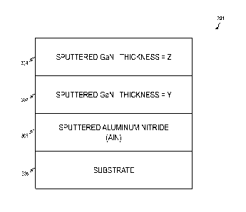
[0059] Figure 3 is a schematic diagram of a GaN structure 301. In some
embodiments,
GaN structure 301 is produced using system 201 of Figure 2 and/or method 101
of Figure 1.
In some embodiments, GaN structure 301 includes a substrate layer 305, a
sputtered
aluminum nitride (A1N) layer 306 on substrate layer 305 (in some such
embodiments, the
thickness of AN layer 306 = X), a sputtered GaN layer 307 on AIN layer 306
where the
thickness of GaN layer 307 =Y (in some such embodiments, GaN layer 307 is
doped (e.g.,
doped with silicon, magnesium, or the like)), and a sputtered GaN layer 308 on
GaN layer
307 where the thickness of GaN layer 308 = Z (in some such embodiments, GaN
layer 308 is
doped (e.g., doped with silicon, magnesium, or the like)).
[0060] Conventional industry systems produce GaN-based devices using
metal-organic
chemical vapor deposition (MOCVD) for the growth of the GaN. In some
embodiments, the
present invention substitutes conventional MOCVD GaN processes with sputtered
GaN,
which allows for: lower wafer bow and thus better wafer/device uniformity due
to the
sputtering, lower process temperature, and less costly chemical usage of NH3
and Ga(CH3)3
and the like. In some embodiments, sputtering processes are more simply
employed and less
costly than MBE processes due to less complex equipment requirements.
[0061] Figure 4 is a schematic diagram of a low-temperature group IIIA-
nitride
sputtering system 401. In some embodiments, sputtering system 401 includes a
vacuum
chamber 405. In some embodiments, chamber 405 includes a wafer holder 406 and
a
sputtering gun 407 (e.g., in some embodiments, sputtering gun 407 is a gallium
sputtering
gun and includes a gallium target). In some embodiments, sputtering gun 407
includes metal
gaskets and other suitable components such that it is suitable to operate in
low temperatures
(e.g., below zero degrees Celsius). In some embodiments, system 401 includes a
cooling
system 408 that cools the gallium target of sputtering gun 407 such that the
gallium target is
maintained in a solid state during sputtering. In some embodiments, cooling
system 408 is
9
Date Recue/Date Received 2020-12-02
operatively coupled to sputtering gun 407 via cold-input line 409 and heat-
output line 410. In
some embodiments, cooling system 408 circulates one or more heat-transfer
fluids through
lines 409 and 410 to maintain the gallium target in a solid state during
sputtering (e.g., in
some such embodiments, the heat-transfer fluid is a cryogenic fluid such as
liquid nitrogen
and/or liquid hydrogen (in some embodiments, liquid nitrogen and/or liquid
hydrogen is used
when sputtering system 401 is used with large wafer and/or wafer platter
production
systems), one or more alcohols, or other suitable heat-transfer fluids). In
some embodiments,
system 401 includes a voltage supply 415 that is connected to system 401 via
wires 499. In
some embodiments, voltage is increased by voltage supply 415 as wafer-size
increases. In
some embodiments, system 401 includes an optical path 420 for in situ closed
or open
process monitoring (in some such embodiments, path 420 is operatively coupled
to a
pyrometer and/or an optical reflectivity system that is computer corrected for
emissivity).
[0062] In some embodiments, the GaN growth processes/systems described
herein are
complementary to epitaxial atomic layer sputtering (EALS). In some
embodiments, EALS is
a process that results in effectively stoichiometric epitaxial growth of a
metal-nitride
compound material upon a substrate using sputtering or reactive sputtering
where the ratio of
the metal (e.g., gallium) to active nitrogen (N) atoms arriving at the surface
of the metal
nitride being formed is periodically varied between metal-rich to N-rich
conditions as
compared to the stoichiometric composition of the metal-nitride compound. In
some
embodiments, this process of switching from metal-rich conditions to metal-
lean conditions is
accomplished by (1) reducing the metal flux to the surface of the metal
nitride being formed,
or (2) increasing the active nitrogen flux, or (3) increasing the temperature
of the substrate (or
exposing the surface of the metal nitride being formed) to increase
evaporation rate (i.e.,
lower the residence time) of the metal adatoms, or any combination of (1) -
(3). In some
embodiments, the metal-rich conditions increase the mobility of adatom by
reducing the
effect of unsatisfied (or dangling) bonds at the surface to enhance surface
migration, which
results in non-columnar step growth and thus higher-quality and smoother
films. In general,
in some embodiments, increased surface migration of adatoms improves crystal
quality of the
deposited materials by assisting the adatoms to incorporate in low-energy
sites on the growth
front. Similarly, in some embodiments, increasing the surface temperature or
applying low-
energy ions can increase surface migration of adatoms to improve thin film
quality.
Accordingly, in some embodiments, the present invention provides EALS. In some
embodiments, this process includes using a separate nitrogen plasma source
(e.g., a radio
frequency (RF) nitrogen source) or even ion beam-assisted deposition.
Date Recue/Date Received 2020-12-02
[0063] Figure 5A is a schematic diagram that illustrates a plurality 501
of different
epitaxial growth modes according to some embodiments of the present invention.
In epitaxial
film growth, deposited material(s) ideally form ordered crystals with atomic
arrangement and
orientation that are determined by the crystallographic structure of the
substrate 505. In some
embodiments, depending on the surface mobility of arriving atoms and the
properties of the
substrate and epitaxial film, different growth modes 510, 520, and/or 530 are
obtained. In
some embodiments, depending on the surface mobility of the arriving atoms on
the substrate
surface, and other factors such as average terrace length of surface steps,
crystal orientation
and defect density of substrate, surface and interface energetic, lattice
mismatch between film
and substrate, the epitaxial growth process 1) starts and progresses in one of
the above
modes, 2) is a mixture of two or more modes, or 3) starts in one mode and then
transitions to
another mode or a mixed growth mode.
[0064] In some embodiments, growth mode 510 (represented by the
progression from
510a to 510b) is referred to as two-dimensional (2D) island growth. In some
embodiments,
in mode 510, small islands nucleate over the surface and laterally grow to
coalesce into a
layer, resulting in many grain boundaries. In some embodiments, growth mode
520
(represented by the progression from 520a to 520b) is referred to as three-
dimensional (3D)
island growth. In some embodiments, in mode 520, small islands nucleate over
the surface
and grow while more islands are formed on top of earlier islands before the
bottom layers are
completed, resulting in increased surface roughness (in some embodiments, mode
520
includes columnar growth). In some embodiments, growth mode 530 (represented
by the
progression from 530a to 530b) is referred to as step-flow growth. In some
embodiments, in
mode 530, atoms arriving on the surface migrate and incorporate at step edges
to complete
layers by step flow (in some embodiments, mode 530 occurs when the surface
diffusion is
large compared to average terrace length).
[0065] Figure 5B is a set 502 of atomic-force microscopy (AFM) images of
GaN
growth. Image 540 shows the smooth GaN with Ga droplets that occurs in some
embodiments where Ga-rich growth conditions are in place. In some embodiments,
epitaxial
atomic layer sputtering (EALS) is implemented during the growth of the GaN
such that there
is a modulation between the Ga-rich growth conditions shown in image 540 and
nitrogen-rich
growth conditions. Image 545 shows the atomic steps of the smooth GaN with no
Ga
droplets that are present in the final state of the GaN film (after the
modulations between the
Ga-rich conditions and the nitrogen-rich conditions), prior to subsequent
deposition. In some
11
Date Recue/Date Received 2020-12-02
embodiments, the root-mean-squared (RMS) roughness of image 540 is about 8
Angstroms.
In some embodiments, the RMS roughness of image 545 is about 2 Angstroms.
[0066] In some embodiments, the present invention generates a material
that includes
GaN on two-dimensional (2D) photonic crystal using one or more of the
processes described
herein. In some embodiments, the GaN on 2D photonic crystal includes repeating
periods of
air/GaN, which are located on a layer of GaN, which is (optionally) located on
a layer of
AN, which is located on sapphire. In some embodiments, the GaN on 2D photonic
crystal
includes repeating periods of air/GaN, which are located on a layer of GaN,
which is
(optionally) located on a layer of AN, which is located on HfN. In some
embodiments, the
GaN on 2D photonic crystal includes repeating periods of air/GaN, which are
located on a
layer of GaN, which is (optionally) located on a layer of AN, which is located
on ZrN. In
some embodiments, the GaN on 2D photonic crystal includes repeating periods of
air/GaN,
which are located on a layer of GaN, which is (optionally) located on a layer
of AN, which is
located on any other suitable Group IIIA nitride. In some embodiments, any of
the GaN
structures are replaced by HfGaN. In some embodiments, any of the GaN
structures are
replaced by ZrGaN.
[0067] In some embodiments, the resulting material thickness of the air
is represented as:
thickness of air void (Tan) = (wavelength)*(12M)/4, where M = Integer
(0,1,2,3,4,5....).
[0068] In some embodiments, the resulting material thickness of GaN
between the air
and sapphire (A1203) is represented as: thickness of GaN between air and A1203
(TGaN) =
(wavelength)*(12M)/(4n), where M is an integer (e.g., 0,1,2,3,4,5....) and n
is the index of
refraction.
[0069] In some embodiments, the GaN on 2D photonic crystal includes
effectively no
carbon compared to GaN formed by MOCVD. In some embodiments, the GaN on 2D
photonic crystal includes effectively no hydrogen compared to GaN formed by
MOCVD.
[0070] In some embodiments, the GaN on 2D photonic crystal includes
effectively
larger epitaxial grains or epi-islands as compared to GaN formed by MOCVD
and/or MBE.
In some embodiments, the GaN on 2D photonic crystal includes epitaxial films
with a
substantially non-columnar structure. In some embodiments, the GaN on 2D
photonic crystal
includes ultra-smooth surfaces due to improved 2D growth. In some embodiments,
the GaN
on 2D photonic crystal includes quantum wells that are smoother than GaN
formed by
conventional processes. In some embodiments, thinner GaN thickness is required
for
dislocation self-annihilation and/or dislocation bending, as compared to
conventional
12
Date Recue/Date Received 2020-12-02
methods of GaN growth. In some embodiments, low-temperature sputtered GaN on
any
material, template, or substrate has significantly different density of misfit
dislocations than
high-temperature growth of GaN. In some embodiments, the GaN on 2D photonic
crystal
includes point-defect density that is substantially different than GaN formed
by conventional
processes. In some embodiments, the GaN on 2D photonic crystal includes lower
wafer bow
than GaN formed by conventional methods. In some embodiments, the GaN on 2D
photonic
crystal includes substantially different stress levels in films, as compared
to GaN formed by
conventional methods. In some such embodiments, the film stress levels are
detectable by
Raman spectroscopy.
[0071] In some embodiments, subsequent epitaxial growth of the GaN
materials of the
present invention results in any suitable light emitting, light detecting,
light harvesting, or
transistor devices (including transistors with vertical carrier flow). In some
embodiments, the
GaN materials of the present invention are used with GaN-based displays (e.g.,
cell phones,
tablets, and the like), GaN-based solar cells, GaN-based detector arrays, GaN-
based very
large scale integration applications, GaN coatings for windows, a GaN-based
high
temperature indium tin oxide (ITO) replacement, and the like. In some
embodiments, wafers
of the GaN materials of the present invention have a diameter that is
approximately six inches
or less. In some embodiments, wafers of the GaN materials of the present
invention have a
diameter that is larger than approximately six inches.
[0072] In some embodiments, the present invention provides a magnetron
reactive
sputtering system for making the GaN materials of the present invention. In
some
embodiments, other suitable sputtering techniques are used such as direct
current (DC) or
radio frequency (RF) sputtering. In some embodiments, the system for making
the GaN
materials of the present invention includes a nitrogen plasma source or an ion
gun. In some
embodiments, a gallium target in a solid state is used and EALS processes are
implemented
to make the GaN materials of the present invention. In some such embodiments,
the solid-
state gallium allows for sputter up, sputter down, or sputter sideways
configurations.
[0073] In some embodiments, the present invention provides a sputter GaN
growth
process that uses a solid gallium source that is located in close proximity
(e.g., less than about
8 inches) to the heated substrate. In some embodiments, the solid gallium
source is located
further away from the substrate. In some embodiments, the wafer substrate is
heated to a
range of 1100-1000 degrees Celsius (C), in some embodiments, a range of 1000-
900 degrees
C, in some embodiments, a range of 900-800 degrees C, in some embodiments, a
range of
13
Date Recue/Date Received 2020-12-02
800-700 degrees C, in some embodiments, a range of 700-600 degrees C, in some
embodiments, a range of 600-500 degrees C, in some embodiments, a range of 500-
400
degrees C, and, in some embodiments, a range of 400 degrees C down to room
temperature.
[0074] In some embodiments, the proximity and type of sputtering gun
(e.g., balanced,
unbalanced, and partially balanced) allow the process to achieve desired add-
atom energy due
to the sputter gun's plasma interaction while minimizing damage to the GaN
film. In some
embodiments, the ionization brought about by the close proximity of the source
and the type
of sputtering gun allows for dislocation bending and/or self-annihilation.
[0075] In some embodiments, the sputtering gun used for the processes of
the present
invention is manufactured with all-metal gasket seals and/or the temperatures
of the N2 used
with the sputtering gun are kept at or below the melting point of gallium so
that the gallium
can be made solid. In some embodiments, heat-transfer liquids such as various
alcohols are
used. In some embodiments, the characteristic dimension of the sputtering
target is larger
than 2 inches in diameter with such a cooling system.
[0076] In some embodiments, there are advantages for a gallium gun to
incorporate a
rotating magnet sputtering gun. In some embodiments, there are other
advantages of using
ringed sputtering targets and/or multiple ring sputtering targets for co-
deposition of
compound materials like indium gallium nitride (InGaN) and/or aluminum gallium
nitride
(AlGaN). In some embodiments, hafnium, zirconium, or silicon are included as
sputtering
targets. In some embodiments, dilute SiH4 in nitrogen is supplied and the gas-
delivery
system contains a double-dilution system. In some embodiments, a ringed
sputtering target
allows for in situ reflectivity measurements. In some embodiments, radio
frequency or direct
current processes are both applicable. In some embodiments, when EALS is used,
varying
between gallium-rich and gallium-lean conditions is accomplished by varying
the
temperature, the pressure, the argon, the nitrogen, the gallium source power,
the growth rate,
or any other suitable variable.
[0077] In some embodiments, the present invention provides a magnetron
sputtering
epitaxial process that includes any one or more of the following steps: (1)
providing any
combination of substrate that includes any number and/or size wafer
substrate(s) or wafer
substrate cassettes that enter a load lock, (2) wherein the substrate is
silicon, sapphire,
GaN/sapphire, A1N/sapphire, GaN/silicon, A1N/silicon or any other suitable
template such as
any other Group IIIA nitride on sapphire or silicon, (3) transferring the
wafer substrate to an
epitaxial chamber via any suitable method or mechanism of manual or robotic
transfer, (4)
14
Date Recue/Date Received 2020-12-02
placing the wafer substrate into an AIN epitaxial sputtering (or other PVD),
MOCVD, or
MBE chamber where AIN is grown to any thickness (columnar or non-columnar) on
the
wafer substrate, (5) transferring the A1N/wafer substrate via any suitable
method or
mechanism of manual or robotic transfer, (6) placing the A1N/substrate wafer
into a GaN
epitaxial sputtering chamber where GaN is grown to any thickness via
sputtering upon the
A1N/wafer substrate (in some embodiments, during this step, the gallium is in
a solid state
and EALS processes are implemented, and, in some embodiments, optional silicon
(Si),
hafnium (Hf), and/or zirconium (Zr) doping is included in the process), (7)
transferring the
sputtered GaN/A1N/wafer substrate via any suitable method or mechanism of
manual or
robotic transfer, (8) placing the sputtered GaN/A1N/wafer substrate into a
Grown-Epitaxial
Metal Mirror (GEMM) sputtering chamber where GEMM growth occurs via sputtering
upon
the sputtered GaN/A1N/wafer substrate (in some such embodiments, the GEMM
growth is
performed according to the descriptions in U.S. Patents 7,915,624, 8,253,157,
and/or
8,890,183, which were introduced above); in some embodiments, the process
repeats steps
5,6,7 in any order or combination as required, (9) optionally growing a layer
of AN to any
suitable thickness via sputtering upon the GEMM, (10) transferring the
sputtered
GEMM/GaN/A1N/wafer substrate via any suitable method or mechanism of manual or
robotic transfer, (11) capping the sputtered GEMM/GaN/A1N/substrate by a final
layer of
sputtered GaN grown to any suitable thickness via sputtering, (12)
transferring the sputtered
GaN/GEMM/GaN/A1N/wafer substrate via any suitable method or mechanism of
manual or
robotic transfer, and (13) placing the sputtered GaN/GEMM/GaN/A1N/wafer
substrate into
an MOCVD, MBE, or sputtering (or other PVD) system for the growth of quantum
well or
quantum wells (also known as the active region) and a P-type layer or P-type
layers.
[0078] In some embodiments, the present invention provides an epitaxial
materials
growth process that includes any one or more of the following steps: (1)
providing any
combination of substrate that includes any number and/or size wafer
substrate(s) or wafer
substrate cassettes that enter a load lock, (2) wherein the substrate is
silicon, sapphire,
GaN/sapphire, A1N/sapphire, GaN/silicon, A1N/silicon or any other suitable
template such as
any other Group IIIA nitride on sapphire or silicon, (3) transferring the
wafer substrate to an
epitaxial chamber via any suitable method or mechanism of manual or robotic
transfer, (4)
placing the wafer substrate into an AIN epitaxial sputtering (or other PVD),
MOCVD, or
MBE chamber where AIN is grown to any thickness (columnar or non-columnar) on
the
wafer substrate, (5) transferring the A1N/wafer substrate via any suitable
method or
mechanism of manual or robotic transfer, (6) placing the A1N/substrate wafer
into a Grown-
Date Recue/Date Received 2020-12-02
Epitaxial Metal Mirror (GEMM) sputter chamber where GEMM growth occurs via
sputtering
upon the A1N/wafer substrate (in some such embodiments, the GEMM growth is
performed
according to the descriptions in U.S. Patents 7,915,624, 8,253,157, and/or
8,890,183, which
were introduced above); in some embodiments, the process repeats steps 1-6 in
any order or
combination as required, (7) growing a layer of AIN to any suitable thickness
via sputtering
upon the GEMM, (8) transferring the sputtered GEMM/A1N/wafer substrate via any
suitable
method or mechanism of manual or robotic transfer, (9) capping the sputtered
GEMM/A1N/wafer substrate by a final layer of sputtered GaN grown to any
suitable
thickness via sputtering upon the GEMM/A1N/wafer substrate (in some such
embodiments,
the gallium is in a solid state and EALS processes are implemented, and, in
some
embodiments, Si, Hf, Zr doping occurs), (10) transferring the sputtered
GaN/GEMM/A1N/wafer substrate via any suitable method or mechanism of manual or
robotic transfer, and (11) placing the sputtered GaN/GEMM/A1N/wafer substrate
into an
MOCVD, MBE, or sputtering (or other PVD) system for the growth of quantum well
or
quantum wells (also known as the active region) and a P-type layer or P-type
layers.
[0079] In some embodiments, the present invention provides an epitaxial
materials
growth process that includes any one or more of the following steps: (1)
providing any
combination of substrate that includes any number and/or size wafer
substrate(s) or wafer
substrate cassettes that enter a load lock, (2) wherein the substrate is
silicon, sapphire,
GaN/sapphire, A1N/sapphire, GaN/silicon, A1N/silicon or any other suitable
template such as
any other Group IIIA nitride on sapphire or silicon, (3) transferring the
wafer substrate to an
epitaxial chamber via any suitable method or mechanism of manual or robotic
transfer, (4)
placing the wafer substrate into a Grown-Epitaxial Metal Mirror (GEMM)
sputtering
chamber where GEMM growth occurs via sputtering upon the wafer substrate (in
some such
embodiments, the GEMM growth is performed according to the descriptions in
U.S. Patents
7,915,624, 8,253,157, and/or 8,890,183, which were introduced above), (5)
transferring the
GEMM/wafer substrate to an epitaxial chamber via any suitable method or
mechanism of
manual or robotic transfer, (6) placing the GEMM/wafer substrate into an AIN
epitaxial
sputtering chamber where AIN is grown to any suitable thickness (columnar or
non-
columnar); in some embodiments, the process repeats steps 4 and 5 as required,
(7) optionally
growing a layer of AIN to any suitable thickness via sputtering upon the GEMM,
(8)
transferring the sputtered GEMM/ALN/GEMM wafer substrate via any suitable
method or
mechanism of manual or robotic transfer, (9) capping the sputtered
GEMM/ALN/GEMM/wafer substrate by a final layer of sputtered GaN grown to any
suitable
16
Date Recue/Date Received 2020-12-02
thickness via sputtering upon the GEMM/ALN/GEMM/wafer substrate (in some such
embodiments, the gallium target used during the sputtering is in a solid state
and EALS
processes are implemented, and, in some embodiments, Si, Hf, Zr doping
occurs), (10)
transferring the sputtered GaN/GEMM/ALN/GEMM/wafer substrate via any suitable
method
or mechanism of manual or robotic transfer, and (11) placing the sputtered
GaN/GEMM/ALN/GEMM/wafer substrate into an MOCVD, MBE, or sputtering (or other
PVD) system for the growth of quantum well or quantum wells (also known as the
active
region) and a P-type layer or P-type layers.
[0080] In some embodiments, the present invention provides an epitaxial
materials
growth process that includes any one or more of the following steps: (1)
providing any
combination of substrate that includes any number and/or size wafer
substrate(s) or wafer
substrate cassettes that enter a load lock, (2) wherein the substrate is
silicon, sapphire,
GaN/sapphire, A1N/sapphire, GaN/silicon, A1N/silicon or any other suitable
template such as
any other Group IIIA nitride on sapphire or silicon, (3) transferring the
wafer substrate to a
sputtering epitaxial chamber via any suitable method or mechanism of manual or
robotic
transfer, (4) growing any Group IIIA nitride material to any suitable
thickness (columnar or
non-columnar) on the wafer substrate, (5) transferring the Group IIIA
nitride/wafer substrate
via any suitable method or mechanism of manual or robotic transfer, (6)
placing the Group
IIIA nitride/wafer substrate into a GEMM sputtering chamber where GEMM growth
occurs
via sputtering upon the Group IIIA nitride/wafer substrate (in some such
embodiments, the
GEMM growth is performed according to the descriptions in U.S. Patents
7,915,624,
8,253,157, and/or 8,890,183, which were introduced above); in some
embodiments, the
process repeats in any order or combination as required, (7) optionally
growing a layer of
AIN or any other Group IIIA nitride to any suitable thickness via sputtering
upon the GEMM,
(8) transferring the sputtered GEMM/Group IIIA nitride/wafer substrate via any
suitable
method or mechanism of manual or robotic transfer, (9) capping the sputtered
GEMM/Group
IIIA nitride/wafer substrate by a final layer of sputtered GaN grown to any
suitable thickness
via sputtering upon the GEMM/Group IIIA nitride/wafer substrate (in some such
embodiments, the gallium is in a frozen/solid state and EALS processes are
implemented,
and, in some embodiments, Si, Hf, Zr doping is implemented), (10) transferring
the sputtered
GaN/GEMM/Group IIIA nitride/wafer substrate via any suitable method or
mechanism of
manual or robotic transfer, and (11) placing the sputtered GaN/GEMM/Group IIIA
nitride/wafer substrate into a MOCVD, MBE, or sputtering (or other PVD) system
for the
17
Date Recue/Date Received 2020-12-02
growth of quantum well or quantum wells (also known as the active region) and
a P-type
layer or P-type layers.
[0081] In some embodiments, the Group IIIA nitride is replaced by any
other Group IIIA
nitride, or any combination of Group IIIA nitride layers and/or compounds. In
addition, in
some embodiments, these materials include silicon (Si), Hf, Zr, and/or
magnesium (Mg). In
some embodiments, a wafer(s) and/or substrate(s) is inserted, moved or
otherwise directly
transferred via any suitable method or mechanism (manual or robotic) within or
between any
combination and/or any number of materials-specific or process-specific
epitaxial sputtering
(or other PVD), MOCVD, or MBE chambers or equipment. In some embodiments, the
processes of the present invention occur in materials-specific sputtering (or
other PVD),
MOCVD, or MBE epitaxial chamber(s) and/or with any combination of optional
wafer
transfer(s) within and between materials-specific sputtering (or other PVD),
MOCVD or
MBE chamber(s). In some embodiments, the processes of the present invention
occur in a
materials-specific sputtering (or other PVD), MOCVD or MBE epitaxial
chamber(s) with no
wafer transfer(s).
[0082] Growing gallium nitride (GaN) films by conventional sputtering
techniques is
typically considered not useful due to the film quality being poor (e.g., GaN
films grown by
conventional sputtering techniques generally have a characteristic X-ray
diffraction (XRD)
rocking curve full width at half maximum value of 620 arcseconds and/or
greater). Since
these sputtered epitaxial grown films are considered lower quality than what
can be produced
by MOCVD or MBE methods, conventional sputtered epitaxial growth techniques
have not
been designed with intentional doping.
[0083] In some embodiments, the present invention provides N-type doping
GaN with a
background electron concentration of about 5x10¹⁶/cm3 (also known
unintentionally doped)
that is intentionally doped with a doping element such as silicon (or titanium
(Ti), zirconium
(Zr), hafnium (Hf), oxygen (0), sulfur (S), selenium (Se) and/or tellurium
(Te)) to achieve an
electron concentration of greater than 5x10¹⁶/cm3 such as lx1018/cm3 to
5x10²⁰/cm3 or higher.
In some embodiments, these intentionally doped materials' electron
concentrations are used
for making ohmic contacts and used as a conductive material.
[0084] In some embodiments, the present invention provides a method for
growing high
quality GaN by sputtering with optional n-type doping that includes any one or
more of the
following: (1) out-gassing the wafer, chamber and wafer holder, (2) GaN
nucleation, wherein
the GaN nucleation includes (a) setting the temperature to allow sufficient
adatom energy so
18
Date Recue/Date Received 2020-12-02
that adatoms are able to find an energetically favorable place in the surface
of the template to
create initial epitaxial growth, (b) setting the chamber vacuum pressure to
allow the
formation of a plasma, (c) supplying plasma gas to the chamber, (d) supplying
nitrogen gas to
the chamber, and (e) providing power to the gun of solid gallium (Ga) target
to provide
gallium and to allow sufficient adatom energy so that adatoms are able to find
an
energetically favorable place in the surface of the template to create initial
epitaxial growth,
wherein the method further includes (3) once nucleation is reached with
minimal thickness,
shutting off the plasma gas source, (4) growing GaN with appropriate
temperatures and gas
flows and Go gun target power to allow for best GaN growth upon GaN layers,
wherein the
GaN sputtering includes doping, and the doping includes (a) co-sputtering of
dopant, (b)
thermal evaporation of dopant, (c) e-beam evaporation of dopant, (d) Ga
mixture with dopant
in sputtering gun, (e) gas injection of dopant reactant including examples of
dilute SiH4,
Si2H6, tetraethylsilane, and/or other reactants holding dopant (Si) in a
carrier gas (H2, N2, Ar,
Xe, He, Kr, Rn, and the like), and (0 ion implantation doping of silicon,
wherein the method
further includes (5) ramping temperature to high enough temperature to remove
any potential
gallium droplets and letting sit until the gallium droplets are gone, and (6)
turning off any of
the above-mentioned variables as needed to remove the wafer.
[0085] The GaN industry is concerned with both the X-ray diffraction
(XRD) 002
(symmetric) and 102 (asymmetric) peak full-width half-maximum (FWHM) values of
Omega
rocking curves for determination of quality for their resulting devices. In
some embodiments,
the present invention provides a sputtering GaN process that enables both 002
and 102 peak
FWHM values to be under 1000 arcseconds, and in some embodiments, below 600
arcseconds, and in some embodiments, below 300 arcseconds, and in some
embodiments,
below 200 arcseconds, and in some embodiments, below 100 arcseconds. In some
embodiments of the invention, the 002 peak FWHM is below 500 arcseconds and
the 102
peak FWHM is below 1000 arcseconds.
[0086] In some embodiments of the invention, the 002 peak FWHM is below
400
arcseconds and the 102 peak FWHM is below 800 arcseconds. In some embodiments,
the
002 peak FWHM is below 300 arcseconds and the 102 peak FWHM is below 600
arcseconds. In some embodiments, the 002 peak FWHM is below 300 arcseconds and
the
102 peak FWHM is below 500 arcseconds. In some embodiments, the 002 peak FWHM
is
below 300 arcseconds and the 102 peak FWHM is below 400 arcseconds. In some
19
Date Recue/Date Received 2020-12-02
embodiments, the 002 peak FWHM is below 250 arcseconds and the 102 peak FWHM
is
below 350 arcseconds.
[0087] In some embodiments, the present invention provides a method that
includes
growing gallium nitride (GaN) via physical vapor deposition (PVD) (e.g., via
sputtering)
such that the grown GaN has an Omega rocking curve full-width half-maximum
(FWHM) X-
ray diffraction measurement for both 002 and 102 peaks that is less than 1000
arcseconds.
[0088] In some embodiments, the present invention provides: (1) co-
sputtering any of Si,
Ti, Zr, Hf, 0, S, Se and/or Te while growing GaN via sputtering, (2) thermal
evaporation of
Si, Ti, Zr, Hf, 0, S, Se and/or Te while growing GaN via sputtering, (3) e-
beam evaporation
is of Si, Ti, Zr, Hf, 0, S, Se and/or Te while growing GaN via sputtering, (4)
Ga mixture with
Si, Ti, Zr, Hf, 0, S, Se and/or Te to grow n-type GaN, (5) gas injection of
dilute SiH4, GeH4,
Si2H6, tetraethylsilane, and/or other reactants holding the already mentioned
elements in
carrier gas (H2, N2, Ar, Xe, He, Kr, Rn...) while growing GaN via sputtering,
and (6) ion
implantation doping of Si, Ti, Zr, Hf, 0, S, Se and/or Te while growing GaN
via sputtering.
In some embodiments, the present invention further includes (7) other group IV
element
doping (e.g., in some embodiments, Ge or Sn), (8) co-doping any combination of
the above
elements, (9) Surfactant (e.g., In) enhanced n-doping, (10) modulated doping
to create special
doping profile or internal electric fields, and/or (11) delta doping any of
the above-mentioned
elements. In some embodiments, the present invention includes applications of
surfactants
for modifying or enhancing growth.
[0089] In some embodiments, the GaN grown using the methods described
herein has an
Omega rocking curve full-width half-maximum (FWHM) X-ray diffraction
measurement (for
the 002 peak and/or the 102 peak) of 0-5 arcseconds; in some embodiments, a
FWHM of 5-
arcseconds; in some embodiments, a FWHM of 10-15 arcseconds; in some
embodiments,
a FWHM of 15-20 arcseconds; in some embodiments, a FWHM of 20-25 arcseconds;
in
some embodiments, a FWHM of 25-30 arcseconds; in some embodiments, a FWHM of
30-
40 arcseconds; in some embodiments, a FWHM of 40-50 arcseconds; in some
embodiments,
a FWHM of 50-100 arcseconds; in some embodiments, a FWHM of 100-150
arcseconds; in
some embodiments, a FWHM of 150-200 arcseconds; in some embodiments, a FWHM of
200-250 arcseconds; in some embodiments, a FWHM of 250-300 arcseconds; in some
embodiments, a FWHM of 300-400 arcseconds; in some embodiments, a FWHM of 400-
500
arcseconds; in some embodiments, a FWHM of 500-600 arcseconds; in some
embodiments, a
FWHM less than 620 arcseconds; in some embodiments, a FWHM of less than 600
Date Recue/Date Received 2020-12-02
arcseconds; in some embodiments, a FWHM of less than 500 arcseconds; in some
embodiments, a FWHM of less than 400 arcseconds; in some embodiments, a FWHM
of less
than 300 arcseconds; in some embodiments, a FWHM of less than 240 arcseconds;
in some
embodiments, a FWHM of less than 200 arcseconds; in some embodiments, a FWHM
of less
than 100 arcseconds; in some embodiments, a FWHM of less than 50 arcseconds;
in some
embodiments, a FWHM of less than 40 arcseconds; in some embodiments, a FWHM of
less
than 30 arcseconds; in some embodiments, a FWHM of less than 27 arcseconds; in
some
embodiments, a FWHM of less than 25 arcseconds; in some embodiments, a FWHM of
less
than 20 arcseconds; in some embodiments, a FWHM of less than 10 arcseconds,
and in some
embodiments, a FWHM of less than 5 arcseconds.
[0090] In some embodiments, the present invention provides a method that
includes
growing gallium nitride (GaN) via physical vapor deposition (PVD) (e.g., via
sputtering)
such that the grown GaN has an Omega rocking curve full-width half-maximum
(FWHM) X-
ray diffraction measurement of less than 620 arcseconds. In some embodiments,
the grown
GaN has an Omega rocking curve full-width half-maximum (FWHM) X-ray
diffraction
measurement of less than 1000 arcseconds. In some embodiments, the method
further
includes during the PVD of the GaN, doping the GaN by co-sputtering at least
one dopant
selected from the group consisting of: silicon (Si), titanium (Ti), zirconium
(Zr), hafnium
(Hf), oxygen (0), sulfur (S), selenium (Se), and tellurium (Te). In some
embodiments, the
method further includes during the PVD of the GaN, doping the GaN by thermally
evaporating at least one selected from the group consisting of: Si, Ti, Zr,
Hf, 0, S, Se, and Te.
In some embodiments, the method further includes during the PVD of the GaN,
doping the
GaN by e-beam evaporating at least one selected from the group consisting of:
Si, Ti, Zr, Hf,
0, S, Se, and Te.
[0091] In some embodiments of the method, the growing of the GaN includes
doping the
GaN to form an n-type GaN using a mixture of Ga and at least one selected from
the group
consisting of: Si, Ti, Zr, Hf, 0, S, Se, and Te. In some embodiments, the
method further
includes during the PVD of the GaN, doping the GaN by: gas injecting at least
one selected
from the group consisting of dilute: Sit14, GeH4, Si2H6, tetraethylsilane,
and/or other
reactants; and holding in a carrier gas (H2, N2, Ar, Xe, He, Kr, Rn, or the
like) and gas
injecting at least one selected from the group consisting of: Si, Ti, Zr, Hf,
0, S, Se, and Te.
In some embodiments, the method further includes during the PVD of the GaN,
doping the
21
Date Recue/Date Received 2020-12-02
GaN by ion-implantation doping at least one selected from the group consisting
of: Si, Ti, Zr,
Hf, 0, S, Se, and Te.
[0092] In some embodiments of the method, the doping of the GaN uses at
least one
dopant selected from the group consisting of germanium (Ge) and tin (Sn)
instead of, or in
addition to, the previously recited elements. In some embodiments, the doping
of the GaN
includes surfactant-enhanced (e.g., In) n-doping. In some embodiments, the
doping of the
GaN includes modulated doping to create a special doping profile or internal
electric field. In
some embodiments, the doping of the GaN includes delta doping any of the
previously
recited elements.
[0093] In some embodiments, the present invention provides a method that
includes
growing gallium nitride (GaN) via physical vapor deposition (PVD) (e.g., in
some
embodiments, via sputtering) such that the grown GaN has an Omega rocking
curve full-
width half-maximum (FWHM) X-ray diffraction measurement (in the 002 plane
and/or the
102 plane) of less than 25 arcseconds.
[0094] In some embodiments, the present invention provides a method that
includes
growing gallium nitride (GaN) via physical vapor deposition (PVD) (e.g., in
some
embodiments, via sputtering) such that the grown GaN has an Omega rocking
curve full-
width half-maximum (FWHM) X-ray diffraction measurement for both 002 and 102
peaks
that is less than 1000 arcseconds.
[0095] In some embodiments, the present invention provides a method that
includes
sputtering epitaxial GaN; and intentional n-type doping during the sputtering.
In some
embodiments of the method, the doping includes co-sputtering silicon (Si). In
some
embodiments, the doping includes thermal evaporation of Si. In some
embodiments, the
doping includes e-beam evaporation of Si. In some embodiments, the sputtering
includes
using a target material that includes a mixture of Ga and Si. In some
embodiments, the
doping includes gas injecting SiH4, Si2H6, tetraethylsilane, and/or other
reactants (in some
embodiments, in dilute portions) with a carrier gas (e.g., H2, N2, Ar, Xe, He,
Kr, Rn, and the
like) holding Si.
[0096] In some embodiments, the doping includes ion-implantation doping
of Si. In
some embodiments, the doping includes sputtering at least one selected from
the group
consisting of silicon (Si), titanium (Ti), zirconium (Zr), hafnium (HO, oxygen
(0), sulfur (S),
selenium (Se), and tellurium (Te). In some embodiments, the doping includes
thermal
evaporation of at least one selected from the group consisting of Si, Ti, Zr,
Hf, 0. S, Se, and
22
Date Recue/Date Received 2020-12-02
Te. In some embodiments, the doping includes e-beam evaporation of at least
one selected
from the group consisting of Si, Ti, Zr, Hf, 0, S, Se, and Te. In some
embodiments, the
sputtering includes using a target material that includes a mixture of Ga and
at least one
selected from the group consisting of Si, Ti, Zr, Hf, 0, S, Se, and Te. In
some embodiments,
the doping includes gas injecting SiH4, Si2H6, tetraethylsilane, and/or other
reactants with a
carrier gas (e.g., H2, N2, Ar, Xe, He, Kr, Rn, and the like) holding at least
one selected from
the group consisting of Si, Ti, Zr, Hf, 0, S, Se, and Te.
[0097] In some embodiments, the doping includes ion-implantation doping
of at least
one dopant selected from the group consisting of Si, Ti, Zr, Hf, 0, S, Se, and
Te. In some
embodiments, the doping includes modulated doping using at least one dopant
selected from
the group consisting of Si, Ti, Zr, Hf, 0, S, Se, and Te to create a special
doping profile or
internal electric fields. In some embodiments, the doping includes delta
doping at least one
dopant selected from the group consisting of Si, Ti, Zr, Hf, 0, S, Se, and Te.
In some
embodiments, the doping includes co-doping at least one dopant selected from
the group
consisting of Si, Ti, Zr, Hf, 0, S, Se, and Te. In some embodiments, the
doping includes
surfactant (e.g., In) enhanced n-doping. In some embodiments, the method
further includes
other group IV element doping (e.g., in some embodiments, Ge or Sn) instead
of, or in
addition to, the elements recited above.
[0098] Figure 6A is a table 601 of thicknesses (in nanometers) for the
AIN and GaN
layers set forth in GaN structure 301 of Figure 3. In some embodiments, each
row of table
601 refers to a range of thicknesses for the AIN layer (e.g., layer 306 of
Figure 3) and a
corresponding range of thicknesses for at least one of the GaN layers (e.g.,
layer 307 and/or
layer 308 of Figure 3). In some embodiments, thickness of the AIN layer is in
a range of
approximately one monolayer to 210 nanometers (nm), and the thickness of the
GaN layer(s)
is in a range of approximately 10 to 20,000 nm.
[0099] Figure 6B is a continuation of table 601.
[00100] Figure 7A is a table 701 showing the Omega rocking curve full-width
half-
maximum (FWHM) X-ray diffraction (XRD) values (in arcseconds) for GaN produced
according to some embodiments of the present invention. Table 701 includes
rocking curve
values for both the 002 (symmetric) and 102 (asymmetric) peaks. In some
embodiments, the
rocking curve values generally decrease with decreasing AIN thickness. In some
embodiments, the smaller rocking curve values are generally more favorable.
23
Date Recue/Date Received 2020-12-02
[00101] Figure 7B is a continuation of table 701. In some embodiments, the
FWHM
value for the GaN 002 peak is in a range of approximately 14.4 to 619
arcseconds, and the
FWHM value for the GaN 102 peak is in a range of approximately 0 to 2515
arcseconds. In
some embodiments, the present invention provides a combination of 002 peak
values below
250 arcseconds and 102 peak values below 550 arcseconds with the AN
thicknesses
presented in table 1201 and sputtering processes (see table 1301 for some FWHM
embodiments provided by the present invention; each row in table 1301 refers
to a range of
FWHM values for the GaN 002 and 102 peaks).
[00102] In some embodiments, the present invention provides a method for
producing a
gallium nitride (GaN)-based device that includes providing a substrate;
sputtering aluminum
nitride (A1N) onto the substrate; and sputtering at least a first layer of GaN
onto the AN such
that the first layer of GaN has an Omega rocking curve full-width half-maximum
(FWHM)
X-ray diffraction (XRD) measurement for a 002 peak that is less than 250
arcseconds and a
FWHM XRD measurement for a 102 peak that is less than 550 arcseconds.
[00103] In some embodiments of the method, the first layer of GaN has a
thickness in a
range of approximately 10 to 20000 nanometers (nm), and wherein the AN has a
thickness in
a range of approximately 5 to 210 nm.
[00104] In some embodiments, the present invention provides a gallium-nitride
(GaN)-
based device that includes a substrate; a first layer of aluminum nitride
(AIN) on the
substrate; and at least a second layer of GaN on the first layer of AIN,
wherein the second
layer of GaN has an Omega rocking curve full-width half-maximum (FWHM) X-ray
diffraction (XRD) measurement for a 002 peak that is less than 250 arcseconds
and a FWHM
XRD measurement for a 102 peak that is less than 550 arcseconds.
[00105] In some embodiments of the apparatus, the first layer of GaN has a
thickness in a
range of approximately 10 to 20000 nanometers (nm), wherein the MN has a
thickness in a
range of approximately one monolayer to 210 nm.
[00106] In some embodiments, the present invention provides a method for
growing
gallium-polar (Ga-polar) gallium nitride (GaN) on sapphire (in some such
embodiments, the
sapphire is substantially a c-plane-oriented sapphire; in some embodiments, a
substantially r-
plane-oriented sapphire; in some embodiments, a substantially m-plane-oriented
sapphire; in
some embodiments, a substantially a-plane-oriented sapphire). In some
embodiments, the
method includes any one or more of the following: (1) substrate preparation
(in some
embodiments, step 1 is optional), wherein the substrate preparation includes
(a) chemical
24
Date Recue/Date Received 2020-12-02
cleaning (epi-ready, and/or degrease, and/or chemical etch), and (b) vacuum
outgassing with
lower pressures and higher temperatures than atmosphere (e.g., in some
embodiments,
vacuum below 1e-6 Torrs, substrate temperature of 800 to 900 degrees C); (2)
surface
nitridation, wherein the surface nitridation includes (a) providing N2 radio
frequency (RF)
plasma with an RF power, an N2 flow rate, and at a substrate temperature for a
duration of
time (e.g., in some embodiments, RF power: 300 ¨ 500 watts (W), N2 flow: 2 - 9
standard
cubic centimeters per minute (SCCM), substrate temperature: 300 to 900 degrees
C, duration:
to 60 minutes), and (b) optionally monitoring reflection high-energy electron
diffraction
(RHEED) during nitridation; (3) forming an AN buffer (in some embodiments,
step 3 is
optional), wherein the forming of the AN buffer includes (a) depositing a
layer of AIN (e.g.,
in some embodiments, 5 nanometers (nm) to 50 nm of AN (or AlGaN)) with an RF
power on
the magnetron gun, a nitrogen flow, an elevated substrate temperature, and an
Al/N flux ratio
(for example, in some embodiments, RF power: 300 ¨ 800 W, N2 flow: 2 to 5
SCCM,
substrate temperature: 700 to 850 C, and Al/N flux slightly greater than 1:1),
(b) in some
embodiments, depositing Al for 5 seconds, then providing 10 seconds of RF
active nitrogen
plasma (once or more), then depositing AN for 1 minute followed by 30 seconds
of
annealing (once or more), then a last N2 anneal (just enough to use extra Al
on surface), (c)
optionally monitoring RHEED pattern change from sapphire to diffused AN to
streaky AIN,
and (d) optionally using optical reflectometry to monitor extra metal anneal
times. In some
embodiments, if the template is AN as described in steps (1) through (3)
above, then gallium
is deposited and subsequently evaporated to remove any oxygen from the AN
surface. In
some embodiments, the method further includes: (4) GaN nucleation, wherein the
GaN
nucleation includes (a) providing 10 to 100 nm of high temperature, N-rich GaN
(for example
in some embodiments, RF power: 300 ¨ 500 W, N2 flow: 2 to 5 SCCM, substrate
temperature: 700 to 850 C, Ga/N flux ratio less than 1:1), (b) optionally
monitoring RHEED
pattern from streaky to extended chevron (two-dimensional (2D) to three-
dimensional (3D)
diffraction), (c) optionally monitoring reflectometry intensity corresponding
to intentional
surface roughening; (5) forming a GaN smoothing layer, wherein the forming of
the GaN
smoothing layer includes (a) providing 100 to 500 nm of high temperature, Ga-
rich GaN (for
example, in some embodiments, RF power: 300 ¨ 500 W, N2 flow: 2 to 5 SCCM,
substrate
temperature: 700 to 850 C, Ga/N flux ratio greater than 1:1), (b) desorbing
extra Ga under N2
(RF plasma off) at an elevated substrate temperature (for example, in some
embodiments,
700 to 800 C), (c) optionally monitoring RHEED pattern from extended chevron
to streaky
(3D to 2D diffraction); (6) forming a thick GaN defect-reduction layer,
wherein the forming
Date Recue/Date Received 2020-12-02
of the GaN defect-reduction layer includes (a) providing 1 to 5 p.m of
slightly Ga-rich GaN
(for example, in some embodiments, RF power: 300 ¨ 500 W, N2 flow: 2 to 5
SCCM,
substrate temperature: 400 to 800 C, Ga/N flux ratio approximately greater
than 1: 1, growth
rate greater than 0.1 p.m/hour), (b) every approximately 15 to 30 minutes,
desorbing extra Go
under N2 (RF plasma off) at an elevated substrate temperature (for example, in
some
embodiments, 700 to 800 C), (c) optionally monitoring RHEED pattern showing
sharper
streaks with increasing GaN thickness, (d) optionally using optical
reflectometry to monitor
growth rate, changes in growth mode, and extra Ga anneal times, (e) optionally
using a
defect-reduction technique such as epitaxial atomic layer sputtering (EALS),
plasma-
enhanced epitaxy, glancing angle ion-assisted growth, thin AN inter-layers and
AlN/GaN
short period superlattice, or any other suitable defect reduction technique,
(f) optionally using
a doping method such as described above (for example, in some embodiments,
dilute
concentration of SiH4 in nitrogen is injected into the chamber).
[00107] In some embodiments, the present invention provides Group IIIA-nitride
AlN/GaN and AlN/AlGaN superlattice (SL) structures used for threading
dislocation (TD)
density reduction (i.e., TD filtering) and/or for strain control and
engineering in GaN and
AlGaN layers and structures grown on sapphire and silicon substrates. In some
such
embodiments, the sputtering techniques described herein (including, in some
embodiments,
epitaxial atomic layer sputtering (EALS)) are used to form the high-quality TD
filtering and
strain-control structures at much lower growth temperatures than conventional
methods. In
some embodiments, the Group IIIA-nitride SL structures include 50 - 100
periods of 3nm -
5nm AN and lOnm - 30nm GaN or AlGaN grown under conditions that promote smooth
interfaces. In some embodiments, the present invention provides SL structures
that include
periodic lattice-matched III-nitride/metal-nitride layers, such as GaN/HfN and
GaN/ZrN SLs
(in some such embodiments, the SL structures additionally have a high out-of-
plane electrical
conductivity compared to AlN/GaN SLs because of very high resistivity of AIN).
[00108] In some embodiments, the present invention provides a method for
producing a
gallium nitride (GaN)-based device that includes providing a substrate
template that includes
aluminum nitride; depositing one or more gallium nitride (GaN) nucleation
layers on the
substrate template; depositing a GaN smoothing layer onto the one or more GaN
nucleation
layers; and depositing a thick GaN defect-reduction layer onto the GaN
smoothing layer.
[00109] In some embodiments, sputter epitaxy provides a plurality of benefits
including
(1) no metal organic precursors, (2) lower process temperatures (as compared
to conventional
26
Date Recue/Date Received 2020-12-02
epitaxy techniques), (3) larger wafers, and (4) superior thermal budget, which
enables
integration.
[001101 In some embodiments, the present invention provides a system and
method that
includes: PVD (e.g., in some embodiments, sputtering) of an AIN Nucleation
Layer (in some
embodiments, 5 minutes of PVD can replace up to about 1.5 hours of MOCVD), PVD
of a
GaN:Hf template (in some embodiments, about 500 nm of GaN:Hf can replace up to
about
51.tm of MOCVD GaN since the conductivity of GaN:Hf is so high), PVD of a
HIN/GaN:Hf
distributed Bragg reflector (DBR) template (in some embodiments, the PVD of
the
HfN/GaN:Hf DBR template enables optical microcavity devices that are lattice-
matched to
GaN, and have 99.99% reflectivity and high conductivity).
[00111] Figure 8A is a schematic diagram of a template and device epitaxy
system 801
for electronics and solid-state lighting (SSL). In some embodiments, system
801 performs
processing on a bare wafer 850 in order to produce a metal-mirror device 860.
In some
embodiments, system 801 includes a plurality of modules 805-810 (in some such
embodiments, each one of the plurality of modules 805-810 is a separate
deposition chamber;
in other embodiments, the plurality of modules 805-810 is contained within a
single
deposition chamber). In some embodiments, system 801 includes an aluminum
nitride
(A1N)-nucleation module 805 configured to generate a nucleation layer of AIN
(in some such
embodiments, the AIN nucleation layer has a thickness of approximately 25
nanometers
(nm)) using one or more of the PVD processes described herein. In some
embodiments,
system 801 further includes a grown-epitaxial metal mirror (GEMM) module 806
configured
to generate one or more GEMM layers (in some such embodiments, the GEMM
layer(s) is
generated according to the descriptions in U.S. Patents 7,915,624, 8,253,157,
and/or
8,890,183, which were introduced above). In some embodiments, system 801
further
includes GaN modules 807, 808, 809, and 810, which are configured to generate
one or more
GaN layers using one or more of the PVD processes described herein (e.g., in
some
embodiments, one or more layers of Hf:GaN are generated at GaN modules 807,
808, 809,
and/or 810).
[00112] Figure 8B is a schematic diagram of a template and device epitaxy
system 802
for electronics and SSL. In some embodiments, system 802 performs processing
on a bare
wafer 850 in order to produce an LED-ready device 870. In some embodiments,
system 802
includes a plurality of modules 805-808 and 820-821 (in some such embodiments,
each one
of the plurality of modules 805-808 and 820-821 is a separate deposition
chamber; in other
27
Date Recue/Date Received 2020-12-02
embodiments, the plurality of modules 805-808 and 820-821 is contained within
a single
deposition chamber),In some embodiments, instead of GaN modules 809 and 810,
system
802 includes MOCVD modules 821 and 822, which are configured to provide MOCVD
processing.
[00113] Figure 9 is a schematic diagram of a template and device epitaxy
process 901 for
electronics and SSL. In some embodiments, process 901 includes steps (A), (B),
and (C). In
some embodiments, step (A) includes generating a nucleation layer of AIN 906
on a sapphire
substrate 905 using one or more of the PVD processes described herein (e.g.,
in some
embodiments, sputtering), wherein the AN nucleation layer 906 has a thickness
of
approximately 25 nm (in some such embodiments, step (A) is performed at module
805 of
Figure 8A). In some embodiments, step (B) includes generating a layer 907 of
Hf:GaN on
the AN nucleation layer 906 using one or more of the PVD processes described
herein (e.g.,
in some embodiments, sputtering). In some embodiments, step (B) is performed
at modules
807, 808, 809, and/or 810 of Figure 8A. In some embodiments, step (C) includes
generating
N periods of alternating layers of Hf:GaN and HfN (e.g., distributed Bragg
reflectors) 908 on
layer 907 based on the GEMM descriptions in U.S. Patents 7,915,624, 8,253,157,
and/or
8,890,183, which were introduced above (in some such embodiments, step (C) is
performed
at GEMM module 806 of Figure 8A). In some embodiments, any one or more of
steps (A),
(B), and (C) further includes generating a layer 920 of n-type GaN and a layer
921 of p-type
GaN/multiple quantum wells (MQWs) using a MOCVD process (in some such
embodiments,
layer 920 has a thickness of approximately 5 micrometers (pm); in other such
embodiments,
layer 920 has a thickness of approximately less than 1 p.m). In some
embodiments, layers
920 and 921 are generated at modules 920 and/or 921 of Figure 8B.
[00114] Figure 10 is a graph 1001 showing n-type carrier concentration (per
cubic
centimeter) versus adatom mobility (cm2N=s) for hafnium-doped gallium nitride
produced
according to some embodiments of the present invention.
[00115] Figure 11 is a graph 1101 showing the X-ray diffraction (XRD) data for
GaN
produced according to some embodiments of the present invention. In some
embodiments,
the Omega rocking curve full-width half-maximum (FWHM) value for the 002 peak
is 300
arcseconds.
[00116] Figure 12 is a schematic diagram of a GaN template structure 1201 for
subsequent LED epitaxial growth. In some embodiments, structure 1201 includes
one or
more indium tin oxide (ITO) replacement layers for use with thin film and
standard light
28
Date Recue/Date Received 2020-12-02
emitting devices. In some embodiments, the ITO replacement layer(s) is
textured (e.g.,
pyramids, domes, 2D photonic crystals, and the like) and includes a GaN doped
with a
transitional metal element to form a textured transitional metal doped GaN
such as Hf:GaN,
Hf: AlGaN, Flf:InGaN, Hf: InGaA1N, or the like. In some embodiments, for p-
side-up
devices, the ITO replacement layer includes a layer 1205 of Hf:GaN placed
directly on top of
the p-type GaN/MQWs layer(s) 921, and a layer 1206 of Si:GaN (in some such
embodiments,
having a thickness of less than 1 um) placed directly below the p-type
GaN/MQWs layer(s)
921. In some embodiments, for p-side-down devices, the ITO replacement layer
includes a
layer 1207 of Hf:GaN placed directly on top of the AIN nucleation layer(s)
906. In some
embodiments, the PVD processes for generating Hf:GaN described herein (e.g.,
sputtering)
have low process temperatures, which allow the ITO layer(s) to be used both
pre and post
epitaxy (accordingly, in some such embodiments, there is no need for tetrakis
dimethylamino
hafnium, which is commonly used in MOCVD systems).
[00117] Figure 13 is a schematic diagram of an epitaxial stack structure 1301
of
GEMM/GaN. In some embodiments, structure 1301 includes a substrate layer 1305
of
sapphire (A1203) and five periods 1306 of alternating layers of GEMM and GaN.
In some
embodiments, structure 1301 is lattice matched for epi-ready growth, highly
conductive (low
resistivity value), and higher in reflectivity than AlN/GaN distributed Bragg
reflectors
(DBRs). In some embodiments, the GEMM growth is performed according to the
descriptions in U.S. Patents 7,915,624, 8,253,157, and/or 8,890,183, which
were introduced
above.
[00118] Figure 14A is a graph 1401 of X-ray diffraction (XRD) data for GaN
produced
according to some embodiments of the present invention. In some embodiments,
the GaN is
lattice matched with a low rocking curve full-width half-maximum (FWHM) value
(e.g., in
some embodiments, a 0.35% mismatch).
[00119] Figure 14B is a graph 1402 of X-ray diffraction (XRD) data for the GaN
produced according to some embodiments of the present invention.
[00120] Figure 14C is a graph 1403 of X-ray diffraction (XRD) data for the GaN
produced according to some embodiments of the present invention.
[00121] Figure 14D is a graph 1404 of X-ray diffraction (XRD) data for the GaN
produced according to some embodiments of the present invention.
29
Date Recue/Date Received 2020-12-02
[00122] Figure 15 is a diagram 1501 of atomic-force microscopy (AFM) data for
GaN on
GEMM produced according to some embodiments of the present invention. In some
embodiments, the GaN on GEMM has an ultra-smooth atomic step surface that
allows
uniform growth of thin quantum wells.
[00123] Figure 16 is a graph 1601 showing a comparison between reflectivity of
GEMM/GaN produced according to some embodiments of the present invention
(solid line)
versus conventional AlN/GaN distributed Bragg reflectors (DBRs) (dashed line).
In some
embodiments, the center wavelength ko is located between 400 nanometers (nm)
and 700 nm,
depending on materials selection and thicknesses.
[00124] Figure 17 is a graph 1701 of estimated sputtering yield for gallium
nitride (GaN)
versus temperature of the gallium target. Graph 1701 shows that, in some
embodiments,
when the gallium target temperature is in region 1705 (i.e., greater than
approximately 14
degrees Celsius (C)), the estimated sputtering yield is temperature sensitive.
In contrast,
graph 1701 shows that, in some embodiments, when the gallium target
temperature is in
region 1706 (i.e., less than approximately 14 degrees C), the estimated
sputtering yield is
temperature insensitive. Graph 1701 further shows that, in some embodiments,
the melting
point of gallium 1799 (approximately 29 degrees C) falls within temperature-
sensitive region
1705. In some embodiments, the present invention cools the gallium target such
that it is
within temperature-insensitive region 1706. In some embodiments, the cooling
of the
gallium target includes providing a temperature gradient across the depth of
the gallium
target such that a first depth of the gallium target is at a first temperature
and a second depth
it at a second temperature.
[00125] In some embodiments, the temperature of the gallium target is kept low
for
reliable repeatable manufacturing as well as high-quality films. In some
embodiments, if the
gallium is a liquid, gallium spitting on the wafer may inhibit manufacturing.
In some
embodiments, if the target is kept at a temperature near gallium's melting
point 1799 (e.g.,
+/- 20 degrees C or more relative to melting point 1799), the yield of ejected
atoms will be
highly dependent on slight changes in the process parameters and the energies
of the ejected
atoms will have a broad distribution.
[00126] In some embodiments, reducing the temperature of the gallium
sputtering target
below 28 degrees Celsius (C) and lower improves the repeatability and quality
of the
resulting gallium nitride (GaN) films. In some embodiments, the quality of the
resulting GaN
films improves down to -40 degrees C, and, in some embodiments, reducing the
temperature
Date Recue/Date Received 2020-12-02
even further (e.g., -200 degrees C) provides additional improvements in GaN
crystal quality.
In some embodiments, the reason for the improved film quality is due to a
refinement of the
gallium purity during the sputtering process where impurities have a lower
sputtering yield at
lower target temperatures. Additionally, in some embodiments, the improvement
is due to a
reduction in "gallium spitting" where plasma gases (e.g., noble gases and
possibly reactive
gases) have a more shallow penetration into the gallium target. In some
embodiments, the
present invention includes noble gases for sputtering and ion sources (e.g.,
in some
embodiments, helium (He), neon (Ne), argon (Ar), krypton (Kr), xenon (Xe),
radon (Rri),
and/or oganesson (Og)).
[00127] In some embodiments of the epitaxial atomic layer sputtering (EALS)
provided
by the present invention, the gallium sputtering target is kept solid and
colder than its melting
point by at least 15 degrees Celsius (C). In some embodiments, the temperature
of the
gallium sputtering target is equal to or between 0 degrees C and 15 degrees C,
inclusive; in
some embodiments, the target temperature is between -15 degrees C and 0
degrees C,
inclusive; in some embodiments, the target temperature is equal to or between -
40 degrees C
and -15 degrees C, inclusive; in some embodiments, the target temperature is
equal to or
between -100 degrees C and -40 degrees C, inclusive; in some embodiments, the
target
temperature is equal to or between -200 degrees C and -100 degrees C,
inclusive; in some
embodiments, the target temperature is lower than -200 degrees C. In some
embodiments,
the gallium sputtering target temperature is between 14 degrees C and -273
degrees C.
[00128] In some embodiments, the present invention provides a method for
producing a
gallium nitride (GaN)-based device that includes providing a substrate
template that includes
aluminum nitride; and depositing a textured transitional metal doped GaN layer
onto the
substrate template.
[00129] Conventional techniques avoid gallium deposition by sputtering due to
gallium's
low melting point (approximately 29 degrees C), especially when the wafer
temperature is
higher than in most applications by hundreds of degrees and the wafer-to-
target distance is
just centimeters away.
[00130] In some embodiments, the present invention provides GaN growth by
sputtering
from a gallium target (solid or liquid) with an XRD 102 peak with a FWHM below
about
3000 arcseconds. In some embodiments, the present invention provides GaN for
use with
high-electron-mobility transistors, wherein the GaN has an XRD 102 peak with a
FWHM
below 1500 arcsec. In some embodiments, the present invention provides GaN for
use with
31
Date Recue/Date Received 2020-12-02
light emitting devices, wherein the GaN has an XRD 102 peak with a FWHM below
600
arcseconds (e.g., 300 arcseconds). In some embodiments, the present invention
provides
smooth non-columnar step growth of GaN by PVD (e.g., sputtering). In some such
embodiments, the gallium target is maintained below 14 degrees C (in some
embodiments,
the gallium target is maintained at subzero Celsius temperatures and non-water
heat-transfer
liquids such as alcohols are used). In some embodiments, the present invention
provides
EALS processes to achieve commercial-grade atomic-force microscopy (AFM),
optical, and
X-ray diffraction (XRD) results.
[00131] In some embodiments, the present invention provides an epitaxial
atomic layer
sputtering (EALS) process (e.g., GaN growth on GaN, AN, nucleation layer
(described
below) or similar template) that includes any one or more of the following:
(1) high-
temperature annealing; (2) at a higher temperature than normal (e.g., by 20
degrees C to 50
degrees C greater), growing Ga:N at a ratio of greater than 1 for 5 to 20
minutes; (3) in a
normal growth mode (e.g., 700 degrees C), growing Ga:N at a ratio of greater
than 1 for 20 to
40 minutes; (4a) stop growth and anneal at 750 degrees C until all excess
gallium is
evaporated and film is smooth (e.g., anneal for 5 to 10 minutes) or (4b)
continue growth but
with Ga:N ratio of less than 1 (in some such embodiments, gallium may be
turned off or the
shutter may be closed); and (5) repeat steps 1 through 4. In some embodiments,
at any time
during the above steps, RF nitrogen is used instead of N2 or NH3 gases while
argon is
supplied directly to the gallium target, and in some embodiments, an ion
source from the
gallium target or a separate ion source is used. In some embodiments, doping
with hafnium
(Hf), zirconium (Zr), silicon (Si), germanium (Ge), magnesium (Mg), copper
(Cu), or any of
the other transitional metals is done during the above steps. In some
embodiments, alloying
GaN with aluminum (Al), indium (In), or any of the other transitional metals
including Hf,
Zr, or scandium (Sc) is done during the above steps.
[00132] In some embodiments, the present invention provides a process for
generating a
nucleation layer on a dissimilar template (e.g., Si, sapphire, hafnium nitride
(HfN), zirconium
nitride (ZrN), zinc oxide (Zn0), glass, or the like), wherein the process
includes any one or
more of the following: (1) thermal cleaning, thermal texturing, chemically
assisted; (2)
nitridation at elevated temperatures by exposing to nitrogen source including
N2, nitrogen
ions, NH3 or the like; and (3) deposition of AIN (optional GaN) to a thickness
in a range of
about 5 nanometers (nm) to 100nm by sputtering. In some embodiments, at any
time during
the above steps, RF nitrogen is used instead of N2 or NH3 gases while argon is
supplied
32
Date Recue/Date Received 2020-12-02
directly to the gallium target, and in some embodiments, an ion source from
the gallium
target or a separate ion source is used. In some embodiments, doping with Hf,
Zr, Si, Ge,
Mg, Cu, or any of the other transitional metals is done during the above
steps. In some
embodiments, alloying GaN with Al, In, or any of the other transitional metals
including, for
example, Hf, Zr, or Sc is done during the above steps.
[00133] Figure 18 is a schematic diagram of a sputtering system 1801. In some
embodiments, system 1801 includes a plurality of gallium (Ga) guns including
Ga gun 1810
(positioned at zero degrees from template 1805), Ga gun 1811 (positioned at 45
degrees from
template 1805), and Ga gun 1812 (positioned 90 degrees from template 1805). In
some
embodiments, system 1801 further includes a plurality of ion sources 1820
and/or 1821. In
some embodiments, template 1805 is rotated between the Ga guns 1810-1812 and
ion sources
1820 and/or 1821. In some embodiments, for manufacturing stability as well as
for the
quality of the group IIIA-nitride films, it is important to provide enough
ions to the surface by
either sputtering gun or ion gun. In some embodiments, the ion gun is replaced
with a photon
source (e.g. ultraviolet) or an electron source. In some embodiments, the ion
source (e.g., ion
source 1820 and/or ion source 1821), whether it be from a dedicated-ion source
or from a
sputtering target, is best when provided at between shallow angle and 90
degrees to the
surface of template 1805. In some embodiments, while these components are in
place, argon
is fed to the sputtering gun and the amount of nitrogen interaction with the
gallium target is
minimized to run processes in a reduced nitrogen poisoning regime.
[00134] In some embodiments, the present invention provides a method for
epitaxially
growing a gallium nitride (GaN) structure that includes providing a substrate;
growing at
least a first GaN layer on a surface of the substrate using a first physical
vapor deposition
(PVD) process (e.g., in some embodiments, sputtering), wherein the first PVD
process
includes: providing a solid gallium target, and maintaining the solid gallium
target at a first
temperature that is less than approximately 29 degrees Celsius.
[00135] In some embodiments of the method, the providing of the substrate
includes
growing an aluminum nitride (A1N) layer on a base of the substrate using a
second PVD
process (e.g., in some embodiments, sputtering) such that the AIN layer forms
the surface of
the substrate. In some embodiments, the first PVD process further includes
epitaxial atomic
layer sputtering (EALS). In some embodiments, the first PVD process further
includes
EALS, wherein the EALS includes heating the substrate. In some embodiments,
the first
PVD process further includes magnetron sputtering. In some embodiments, the
first
33
Date Recue/Date Received 2020-12-02
temperature is less than approximately 15 degrees Celsius. In some
embodiments, the
maintaining of the solid gallium target at the first temperature includes
fluid-convection
cooling the solid gallium target using an alcohol-based fluid. In some
embodiments, the first
GaN layer has an Omega rocking curve full-width half-maximum (FWHM) X-ray
diffraction
measurement for both 002 and 102 peaks that is less than approximately 1000
arcseconds.
[00136] In some embodiments, the present invention provides a method for
growing a
gallium nitride (GaN) structure that includes providing a substrate; and
growing at least a first
GaN layer on a surface of the substrate using a first physical vapor
deposition (PVD) process
(e.g., in some embodiments, a first sputtering process), wherein the first PVD
process
includes: providing a solid gallium target, wherein the providing of the solid
gallium target
includes maintaining the solid gallium target at a first temperature, and
implementing
epitaxial atomic layer sputtering (EALS) of the at least first GaN layer such
that the growing
of the at least first GaN layer includes non-columnar step growth of the at
least first GaN
layer.
[00137] In some embodiments, the present invention provides a system for
growing a
gallium nitride (GaN) structure that includes a load lock configured to load a
substrate wafer
into the system and remove the GaN structure from the system; and a plurality
of deposition
modules, wherein the plurality of deposition modules includes a GaN-deposition
module
configured to grow at least a first GaN layer on a surface of the substrate
wafer via a first
physical vapor deposition (PVD) process (e.g., in some embodiments, a first
sputtering
process), wherein the GaN-deposition module includes a solid gallium target
that is
maintained at a first temperature, and wherein the first PVD process includes
epitaxial atomic
layer sputtering (EALS) of the at least first GaN layer such that non-columnar
step growth of
the at least first GaN layer occurs.
[00138] In some embodiments, the present invention provides a method for
growing a
gallium nitride (GaN) structure that includes providing a substrate; and
growing at least a first
GaN layer on a surface of the substrate using a first sputtering process,
wherein the first
sputtering process includes: providing a gallium target, and implementing
epitaxial atomic
layer sputtering (EALS) such that the growing of the at least first GaN layer
includes non-
columnar step growth of the at least first GaN layer.
[00139] In some embodiments, the implementing of the MEE includes controlling
a ratio
of gallium-to-nitrogen to be greater than 1-to-1 for at least a first time
period of the first
34
Date Recue/Date Received 2020-12-02
sputtering process. In some embodiments of the method, the implementing of the
MEE
includes introducing nitrogen via a radio frequency (RF) nitrogen source.
[00140] In some embodiments of the method, the first sputtering process
further includes
doping the at least first GaN layer with silicon (Si). In some embodiments,
the first
sputtering process further includes doping the at least first GaN layer by gas
injecting a
reactant with a carrier gas holding silicon (Si).
[00141] In some embodiments of the method, the gallium target is a solid
gallium target,
wherein the first sputtering process further includes maintaining the solid
gallium target at a
first temperature that is less than approximately 15 degrees Celsius. In some
embodiments,
the gallium target is a solid gallium target, wherein the first sputtering
process further
includes maintaining the solid gallium target at a first temperature, and
wherein the
maintaining of the solid gallium target at the first temperature includes
fluid-convection
cooling the solid gallium target using an alcohol-based fluid.
[00142] In some embodiments of the method, the providing of the substrate
includes
growing an aluminum nitride (A1N) layer on a base of the substrate using a
second sputtering
process such that the AIN layer forms the surface of the substrate. In some
embodiments, the
method further includes growing a grown-epitaxial metal mirror (GEMM) on the
at least first
GaN layer. In some embodiments, the method further includes growing a grown-
epitaxial
metal mirror (GEMM) on the at least first GaN layer, wherein the GEMM includes
alternating layers of hafnium (Hf):GaN and hafnium nitride (HfN). In some
embodiments,
the method further includes growing a grown-epitaxial metal mirror (GEMM) on
the at least
first GaN layer, wherein the GEMM includes alternating layers of hafnium
(Hf):GaN and
hafnium nitride (HfN); and growing at least a first quantum well on a surface
of the GEMM
using a metal-organic chemical vapor deposition (MOCVD) process. In some
embodiments,
the first sputtering process further includes magnetron sputtering. In some
embodiments, the
at least first GaN layer has an Omega rocking curve full-width half-maximum
(FWHM) X-
ray diffraction measurement for both 002 and 102 peaks that is less than
approximately 1000
arcseconds. In some embodiments, the at least first GaN layer has an Omega
rocking curve
full-width half-maximum (FWHM) X-ray diffraction measurement for a 002 peak
that is in a
range of about 10 arcseconds to about 2500 arcseconds.
[00143] In some embodiments, the present invention provides a system for
growing a
gallium nitride (GaN) structure that includes a load lock configured to load a
substrate wafer
into the system and remove the GaN structure from the system; and a
plurality of
Date Recue/Date Received 2020-12-02
deposition chambers, wherein the plurality of deposition chambers includes a
GaN-deposition
chamber configured to grow at least a first GaN layer on a surface of the
substrate wafer via a
first sputtering process, and wherein the first sputtering process includes
epitaxial atomic
layer sputtering (EALS) of the at least first GaN layer such that non-columnar
step growth of
the at least first GaN layer occurs.
[00144] In some embodiments, the system further includes a wafer-handling
mechanism
configured to automatically transfer the substrate wafer between the plurality
of deposition
chambers. In some embodiments, the plurality of deposition chambers includes
an aluminum
nitride (A1N)-deposition chamber configured to grow an AIN layer on a base of
the substrate
wafer via a second sputtering process such that the AIN layer forms the
surface of the
substrate wafer. In some embodiments, the plurality of deposition chambers
includes a
grown-epitaxial metal minor (GEMM)-deposition chamber configured to grow a
GEMM on
the at least first GaN layer. In some embodiments, the GaN-deposition chamber
includes a
solid gallium target that is maintained at a first temperature, and wherein
the first temperature
is less than approximately 15 degrees Celsius. In some embodiments, the GaN-
deposition
chamber further includes: a solid gallium target that is maintained at a first
temperature; and a
fluid-convection cooler configured to cool the solid gallium target via an
alcohol-based fluid.
[00145] In some embodiments, the GaN-deposition chamber is further configured
to dope
the at least first GaN layer with silicon (Si). In some embodiments, the GaN-
deposition
chamber is further configured to grow the at least first GaN layer such that
the at least first
GaN layer has an Omega rocking curve full-width half-maximum (FWHM) X-ray
diffraction
measurement for both 002 and 102 peaks that is less than approximately 1000
arcseconds. In
some embodiments, the GaN-deposition chamber is further configured to grow the
at least
first GaN layer such that the at least first GaN layer has an Omega rocking
curve full-width
half-maximum (FWHM) X-ray diffraction measurement for a 002 peak that is in a
range of
about 10 arcseconds to about 2500 arcseconds.
[00146] In some embodiments, the plurality of deposition chambers further
includes: an
aluminum nitride (A1N)-deposition chamber configured to grow an AIN layer on a
base of the
substrate wafer via a second sputtering process such that the AIN layer forms
the surface of
the substrate wafer; a grown-epitaxial metal mirror (GEMM)-deposition chamber
configured
to grow a GEMM on the at least first GaN layer, wherein the GEMM includes
alternating
layers of hafnium (Hf):GaN and hafnium nitride (HfN); and a metal-organic
chemical vapor
36
Date Recue/Date Received 2020-12-02
deposition (MOCVD) chamber configured to grow at least a first quantum well on
a surface
of the GEMM.
[00147] In some embodiments, the present invention provides a gallium-nitride
structure
that includes a substrate; and at least a first gallium nitride (GaN) layer
grown on a surface of
the substrate, wherein the at least first GaN layer has an Omega rocking curve
full-width half-
maximum (FWHM) X-ray diffraction measurement for both 002 and 102 peaks that
is less
than approximately 1000 arcseconds (in some embodiments, the at least first
GaN layer has
an Omega rocking curve full-width half-maximum (FWHM) X-ray diffraction
measurement
for a 002 peak that is in a range of about 10 arcseconds to about 2500
arcseconds).
[00148] In some embodiments, the structure further includes an aluminum
nitride (A1N)
layer grown on a base of the substrate such that the AN layer forms the
surface of the
substrate. In some embodiments, the structure further includes a grown-
epitaxial metal
mirror (GEMM) grown on a surface of the at least first GaN layer. In some
embodiments,
the substrate includes sapphire, the structure further including an aluminum
nitride (A1N)
layer on a base of the substrate such that the AIN layer forms the surface of
the substrate; a
grown-epitaxial metal mirror (GEMM) grown on a surface of the at least first
GaN layer,
wherein the GEMM includes alternating layers of hafnium (HO: GaN and hafnium
nitride
(HfN); a layer of n-type GaN grown on a surface of the GEMM; and a layer of p-
type
GaN/multiple quantum wells (MQWs) grown on the layer of n-type GaN.
[00149] In some embodiments, the present invention provides a system for
growing a
gallium nitride (GaN) structure that includes means for loading a substrate
wafer into the
system; and means for sputtering at least a first GaN layer on a surface of
the substrate wafer,
wherein the means for sputtering the at least first GaN layer includes means
for implementing
epitaxial atomic layer sputtering (EALS) such that non-columnar step growth of
the at least
first GaN layer occurs.
[00150] In some embodiments of the system, the means for sputtering includes
means for
doping the at least first GaN layer with silicon (Si). In some embodiments,
the system further
includes means for growing an aluminum nitride (A1N) layer on a base of the
substrate such
that the AN layer forms the surface of the substrate. In some embodiments, the
system
further includes means for growing a grown-epitaxial metal mirror (GEMM) on
the at least
first GaN layer, wherein the GEMM includes alternating layers of hafnium
(Hf):GaN and
hafnium nitride (HfN). In some embodiments, the system further includes: means
for
growing a grown-epitaxial metal mirror (GEMM) on the at least first GaN layer,
wherein the
37
Date Recue/Date Received 2020-12-02
GEMM includes alternating layers of hafnium (HO:GaN and hafnium nitride (HfN);
and
means for growing at least a first quantum well on a surface of the GEMM.
[00151] In some embodiments, the present invention provides a method for
growing a
gallium nitride (GaN) structure that includes providing a template; and
growing at least a first
GaN layer on the template using a first sputtering process, wherein the first
sputtering process
includes: controlling a temperature of a sputtering target, and modulating
back and forth
between a gallium-rich condition and a gallium-lean condition, wherein the
gallium-rich
condition includes a gallium-to-nitrogen ratio having a first value that is
greater than 1, and
wherein the gallium-lean condition includes the gallium-to-nitrogen ratio
having a second
value that is less than 1.
[00152] In some embodiments of the method, the first sputtering process
further includes
introducing nitrogen via a radio frequency (RF) nitrogen source. In some
embodiments, the
first sputtering process further includes doping the at least first GaN layer
with silicon (Si).
In some embodiments, the first sputtering process further includes doping the
at least first
GaN layer by gas injecting a reactant with a carrier gas holding silicon (Si).
In some
embodiments, the sputtering target is a solid gallium target, wherein the
controlling of the
temperature of the solid gallium target includes maintaining the temperature
at a first
temperature value that is less than approximately 14 degrees Celsius. In some
embodiments,
the sputtering target is a solid gallium target, and wherein the controlling
of the temperature
of the solid gallium target includes fluid-convection cooling the solid
gallium target using an
alcohol as a heat-transfer fluid.
[00153] In some embodiments of the method, the providing of the template
includes
growing an aluminum nitride (A1N) layer on the template. In some embodiments,
the
providing of the template includes growing an aluminum nitride (A1N) layer on
the template
using a second sputtering process. In some embodiments, the providing of the
template
includes growing a first aluminum nitride (A1N) layer on the template using a
second
sputtering process, wherein the method further includes growing a second
aluminum nitride
(A1N) layer on the at least first GaN layer using the second sputtering
process; and growing a
second GaN layer on the second A1N layer using the first sputtering process.
[00154] In some embodiments, the method further includes growing a grown-
epitaxial
metal mirror (GEMM) on the at least first GaN layer, wherein the GEMM includes
alternating layers of hafnium (Hf):GaN and hafnium nitride (HfN). In some
embodiments,
the method further includes growing a grown-epitaxial metal mirror (GEMM) on
the at least
38
Date Recue/Date Received 2020-12-02
first GaN layer, wherein the GEMM includes alternating layers of hafnium
(Hf):GaN and
hafnium nitride (MN); and growing at least a first quantum well on a surface
of the GEMM
using a metal-organic chemical vapor deposition (MOCVD) process. In some
embodiments,
the first sputtering process further includes magnetron sputtering. In some
embodiments, the
at least first GaN layer has an Omega rocking curve full-width half-maximum
(FWHM) X-
ray diffraction measurement for a 002 peak that is in a range of about 10
arcseconds to about
2500 arcseconds.
[00155] In some embodiments, the present invention provides a system for
growing a
gallium nitride (GaN) structure that includes a load lock configured to load a
substrate wafer
into the system and remove the GaN structure from the system; and a
plurality of
deposition chambers, wherein the plurality of deposition chambers includes a
GaN-deposition
chamber configured to grow at least a first GaN layer on a template that
includes the substrate
wafer via a first sputtering process, and wherein the first sputtering process
includes a
modulation back and forth between a gallium-rich condition and a gallium-lean
condition,
wherein the gallium-rich condition includes a gallium-to-nitrogen ratio having
a first value
that is greater than 1, and wherein the gallium-lean condition includes the
gallium-to-nitrogen
ratio having a second value that is less than 1.
[00156] In some embodiments, the system further includes a wafer-handling
mechanism
configured to automatically transfer the template between the plurality of
deposition
chambers. In some embodiments, the plurality of deposition chambers includes
an aluminum
nitride (A1N)-deposition chamber configured to grow an AIN layer on the
substrate wafer to
form the template via a second sputtering process. In some embodiments, the
plurality of
deposition chambers includes a grown-epitaxial metal mirror (GEMM)-deposition
chamber
configured to grow a GEMM on the at least first GaN layer. In some
embodiments, the GaN-
deposition chamber includes a solid gallium target that is maintained at a
first temperature,
and wherein the first temperature is less than approximately 14 degrees
Celsius. In some
embodiments, the GaN-deposition chamber further includes: a
solid gallium target that
is maintained at a first temperature; and a fluid-convection cooler configured
to cool the solid
gallium target via an alcohol heat-transfer fluid. In some embodiments, the
GaN-deposition
chamber is further configured to dope the at least first GaN layer with
silicon (Si). In some
embodiments, the GaN-deposition chamber is further configured to grow the at
least first
GaN layer such that the at least first GaN layer has an Omega rocking curve
full-width half-
maximum (FWHM) X-ray diffraction measurement for a 002 peak that is in a range
of about
39
Date Recue/Date Received 2020-12-02
arcseconds to about 2500 arcseconds. In some embodiments, the plurality of
deposition
chambers further includes: an aluminum nitride (A1N)-deposition chamber
configured to
grow an AIN layer on the substrate wafer to form the template via a second
sputtering
process; a grown-epitaxial metal mirror (GEMM)-deposition chamber configured
to grow a
GEMM on the at least first GaN layer, wherein the GEMM includes alternating
layers of
hafnium (Hf):GaN and hafnium nitride (HfN); and a metal-organic chemical vapor
deposition
(MOCVD) chamber configured to grow at least a first quantum well on a surface
of the
GEMM.
[00157] In some embodiments, the present invention provides a gallium-nitride
structure
that includes a template; and at least a first gallium nitride (GaN) layer
grown on the
template, wherein the at least first GaN layer has an Omega rocking curve full-
width half-
maximum (FWHM) X-ray diffraction measurement for a 002 peak that is in a range
of about
10 arcseconds to about 2500 arcseconds.
[00158] In some embodiments, the template includes an aluminum nitride (A1N)
layer
grown on a substrate. In some embodiments, the structure further includes a
grown-epitaxial
metal mirror (GEMM) grown on a surface of the at least first GaN layer. In
some
embodiments, the template includes an aluminum nitride (A1N) layer grown on a
sapphire
substrate, the structure further including a grown-epitaxial metal mirror
(GEMM) grown on a
surface of the at least first GaN layer, wherein the GEMM includes alternating
layers of
hafnium (Hf):GaN and hafnium nitride (HfN); a layer of n-type GaN grown on a
surface of
the GEMM; and a layer of p-type GaN/multiple quantum wells (MQWs) grown on the
layer
of n-type GaN.
[00159] In some embodiments, the present invention provides a system for
growing a
gallium nitride (GaN) structure that includes means for loading a substrate
wafer into the
system; and means for sputtering at least a first GaN layer on a template that
includes the
substrate wafer, wherein the means for sputtering the at least first GaN layer
includes means
for modulating back and forth between a gallium-rich condition and a gallium-
lean condition,
wherein the gallium-rich condition includes a gallium-to-nitrogen ratio having
a first value
that is greater than 1, and wherein the gallium-lean condition includes the
gallium-to-nitrogen
ratio having a second value that is less than 1.
[00160] In some embodiments of the system, the means for sputtering includes
means for
doping the at least first GaN layer with silicon (Si). In some embodiments,
the system further
includes means for growing an aluminum nitride (A1N) layer on the substrate
wafer to form
Date Recue/Date Received 2020-12-02
the template. In some embodiments, the system further includes means for
growing a grown-
epitaxial metal mirror (GEMM) on the at least first GaN layer, wherein the
GEMM includes
alternating layers of hafnium (HO:GaN and hafnium nitride (HfN). In some
embodiments,
the system further includes means for growing a grown-epitaxial metal mirror
(GEMM) on
the at least first GaN layer, wherein the GEMM includes alternating layers of
hafnium
(Hf):GaN and hafnium nitride (HfN); and means for growing at least a first
quantum well on
a surface of the GEMM.
[00161] In some embodiments, the present invention provides a method for
growing a
gallium nitride (GaN) structure that includes providing a template; and
growing at least a first
GaN layer on the template using a first sputtering process, wherein the first
sputtering process
includes: providing a gallium sputtering target, wherein the gallium
sputtering target has a
depth, and maintaining a temperature of the gallium sputtering target at a
first temperature
value that is less than approximately 14 degrees Celsius. In some embodiments,
the
maintaining of the temperature of the gallium sputtering target includes
providing a
temperature gradient across the depth of the gallium sputtering target.
[00162] In some embodiments, the present invention provides a method for
growing a
gallium nitride (GaN) structure that includes providing a template having a
surface; and
growing at least a first GaN layer on the template using a first sputtering
process, wherein the
first sputtering process includes: modulating back and forth for at least a
first oscillation
between a gallium-rich condition on the surface of the template and a gallium-
lean condition
on the surface of the template, wherein the gallium-rich condition includes a
gallium-to-
nitrogen ratio having a first value that is greater than 1, and wherein the
gallium-lean
condition includes the gallium-to-nitrogen ratio having a second value that is
less than the
first value. In some embodiments, the modulating back and forth includes
modulating back
and forth for a plurality of oscillations including the first oscillation. In
some embodiments,
the at least first GaN layer has an Omega rocking curve full-width half-
maximum (FWHM)
X-ray diffraction measurement for a 102 peak that is in a range of about 10
arcseconds to
about 2500 arcseconds.
[00163] In some embodiments, the present invention provides a method for
growing a
gallium nitride (GaN) structure that includes providing a template; and
growing at least a first
GaN layer on the template using a first sputtering process, wherein the first
sputtering process
includes: providing a gallium sputtering target, wherein the gallium
sputtering target has a
depth, and maintaining a temperature of the gallium sputtering target at a
first temperature
41
Date Recue/Date Received 2020-12-02
value that is less than approximately 14 degrees Celsius. In some embodiments,
the at least
first GaN layer has an Omega rocking curve full-width half-maximum (FWHM) X-
ray
diffraction measurement for a 102 peak that is in a range of about 10
arcseconds to about
2500 arcseconds. In some embodiments, the maintaining of the temperature of
the gallium
sputtering target includes providing a temperature gradient across the depth
of the gallium
sputtering target.
[00164] In some embodiments, the present invention provides a method for
growing a
gallium nitride (GaN) structure that includes providing a template; growing a
first aluminum
nitride (A1N) layer on the template using a first sputtering process; and
growing a first GaN
layer on the first AIN layer using a second sputtering process. In some
embodiments, the
method further includes growing a second AN layer on the first GaN layer using
the first
sputtering process; and growing a second GaN layer on the second MN layer
using the
second sputtering process. In some embodiments, the first GaN layer has an
Omega rocking
curve full-width half-maximum (FWHM) X-ray diffraction measurement for a 102
peak that
is in a range of about 10 arcseconds to about 2500 arcseconds.
[00165] In some embodiments, the present invention provides a method for
growing a
gallium nitride (GaN) structure that includes providing a template having a
surface; and
growing at least a first GaN layer on the template using a first sputtering
process, wherein the
first sputtering process includes: growing the at least first GaN layer under
at least two
conditions, wherein the two conditions include a gallium-rich condition and a
gallium-lean
condition, wherein the gallium-rich condition includes a gallium-to-nitrogen
ratio having a
first value that is greater than 1, wherein the gallium-lean condition
includes the gallium-to-
nitrogen ratio having a second value that is less than the first value;
alternating between the
two conditions for at least a first growing under a first of the two
conditions, a second
growing under a second of the two conditions after the first growing, and a
third growing
under the first of the two conditions after the second growing. In some
embodiments, the
alternating between the two conditions further includes a fourth growing under
the second of
the two conditions after the third growing, and a fifth growing under the
first of the two
conditions after the fourth growing. In some embodiments, the first value of
the gallium-to-
nitrogen ratio is at least ten percent larger than the second value of the
gallium-to-nitrogen
ratio. In some embodiments, the first value of the gallium-to-nitrogen ratio
is at least fifty
percent larger than the second value of the gallium-to-nitrogen ratio. In some
embodiments,
42
Date Recue/Date Received 2020-12-02
the first value of the gallium-to-nitrogen ratio is at least two times larger
than the second
value of the gallium-to-nitrogen ratio.
[00166] In some embodiments, the present invention provides a method for
growing a
gallium nitride (GaN) structure that includes providing a template; growing a
first aluminum
nitride (A1N) layer on the template using a first sputtering process; and
growing a first GaN
layer on the first AIN layer using a second sputtering process. In some
embodiments, the
method further includes growing a second AN layer on the first GaN layer using
the first
sputtering process; and growing a second GaN layer on the second MN layer
using the
second sputtering process. In some embodiments, the first GaN layer has an
Omega rocking
curve full-width half-maximum (FWHM) X-ray diffraction measurement for a 102
peak that
is in a range of about 10 arcseconds to about 2500 arcseconds. In some
embodiments, the
method further includes growing a second AN layer on the first GaN layer using
the first
sputtering process; growing a second GaN layer on the second AN layer using
the second
sputtering process; and growing one or more layers of AlGa0,0N on the second
GaN layer,
where x is between 0 and 1, inclusive. In some embodiments, the method further
includes
growing a second AN layer on the first GaN layer using the first sputtering
process; growing
a second GaN layer on the second AN layer using the second sputtering process;
and
growing one or more layers of AlGati,oN on the second GaN layer, where x
varies with
depth and is between 0 and 1, inclusive. In some embodiments, the method
further includes
growing a second AN layer on the first GaN layer using the first sputtering
process; growing
a second GaN layer on the second AN layer using the second sputtering process;
and
growing one or more layers of compounds on the second GaN layer, wherein the
compounds
include one or more selected from the group consisting of hafnium nitride
(HfN), zirconium
nitride (ZrN), aluminum nitride (A1N), gallium nitride (GaN), and scandium
nitride (ScN). In
some embodiments, the method further includes growing one or more layers of
AlõGa(l_x)N
on the first GaN layer, where x is between 0 and 1, inclusive. In some
embodiments, first
sputtering process further includes doping the at least first GaN layer with
silicon (Si). In
some embodiments, the method further includes growing one or more layers of
AlõGa(l_x)N
on the first GaN layer, where x is between 0 and 1, inclusive. In some
embodiments, the
method further includes growing one or more layers of AlGa(l,)N on the first
GaN layer,
where x varies with depth and is between 0 and 1, inclusive. In some
embodiments, the
method further includes growing one or more layers of compounds on the first
GaN layer,
wherein the compounds include one or more selected from the group consisting
of hafnium
43
Date Recue/Date Received 2020-12-02
nitride (HfN), zirconium nitride (ZrN), aluminum nitride (AIN), gallium
nitride (GaN), and
scandium nitride (ScN).
[00167] In some embodiments, the present invention provides a system for
growing a
gallium nitride (GaN) structure that includes a load lock configured to load a
substrate wafer
into the system and remove the GaN structure from the system; and a plurality
of deposition
chambers, wherein the plurality of deposition chambers includes a first GaN-
deposition
chamber configured to grow at least a first GaN layer, via a first sputtering
process, on a
template that includes the substrate wafer, wherein the first GaN-deposition
chamber includes
a gallium sputtering target, wherein the gallium sputtering target has a
depth, and wherein the
GaN-deposition chamber is further configured to maintain a temperature of the
gallium
sputtering target at a first temperature value that is less than approximately
14 degrees
Celsius.
[00168] In some embodiments, the system further includes a wafer-handling
mechanism
configured to automatically transfer the template between the plurality of
deposition
chambers. In some embodiments, the plurality of deposition chambers includes
an aluminum
nitride (A1N)-deposition chamber configured to grow an AN layer, via a second
sputtering
process, on the substrate wafer to form the template. In some embodiments, the
plurality of
deposition chambers includes a grown-epitaxial metal mirror (GEMM)-deposition
chamber
configured to grow a GEMM on the at least first GaN layer. In some
embodiments, the
system further includes a fluid-convection cooler configured to cool the
gallium sputtering
target via an alcohol heat-transfer fluid. In some embodiments, the GaN-
deposition chamber
is further configured to maintain a temperature gradient across the depth of
the gallium
sputtering target. In some embodiments, the plurality of deposition chambers
includes a
metal-organic chemical vapor deposition (MOCVD) chamber. In some embodiments,
the
GaN-deposition chamber is further configured to dope the at least first GaN
layer with silicon
(Si).
[00169] In some embodiments, the present invention provides a gallium-nitride
structure
that includes a template; and at least a first gallium nitride (GaN) layer
grown on the
template, wherein the at least first GaN layer has an Omega rocking curve full-
width half-
maximum (FWHM) X-ray diffraction measurement for a 102 peak that is in a range
of about
arcseconds to about 2500 arcseconds. In some embodiments, the template
includes an
aluminum nitride (AN) layer grown on a sapphire substrate, the structure
further including a
grown-epitaxial metal mirror (GEMM) grown on a surface of the at least first
GaN layer,
44
Date Recue/Date Received 2020-12-02
wherein the GEMM includes alternating layers of hafnium (Hf):GaN and hafnium
nitride
(HfN); a layer of n-type GaN grown on a surface of the GEMM; and a layer of p-
type
GaN/multiple quantum wells (MQWs) grown on the layer of n-type GaN.
[00170] It is specifically contemplated that the present invention includes
embodiments
having combinations and subcombinations of the various embodiments and
features that are
individually described herein (i.e., rather than listing every combinatorial
of the elements, this
specification includes descriptions of representative embodiments and
contemplates
embodiments that include some of the features from one embodiment combined
with some of
the features of another embodiment). Further, some embodiments include fewer
than all the
components described as part of any one of the embodiments described herein.
Still further,
it is specifically contemplated that the present invention includes
embodiments having
combinations and subcombinations of the various embodiments described herein
and the
various embodiments described by the related applications and publications in
paragraphs
above of the present application.
[00171] It is
to be understood that the above description is intended to be illustrative,
and
not restrictive. Although numerous characteristics and advantages of various
embodiments as
described herein have been set forth in the foregoing description, together
with details of the
structure and function of various embodiments, many other embodiments and
changes to
details will be apparent to those of skill in the art upon reviewing the above
description. The
scope of the invention should be, therefore, determined with reference to the
appended
claims, along with the full scope of equivalents to which such claims are
entitled. In the
appended claims, the terms "including" and "in which" are used as the plain-
English
equivalents of the respective terms "comprising" and "wherein," respectively.
Moreover, the
terms "first," "second," and "third," etc., are used merely as labels, and are
not intended to
impose numerical requirements on their objects.
Date Recue/Date Received 2020-12-02