Note: Descriptions are shown in the official language in which they were submitted.
CA 03025801 2018-11-28
WO 2016/191852
PCT/CA2016/000162
-1-
IMAGE SENSOR CIRCUITS AND METHODS
CROSS-REFERENCE TO RELATED APPLICATIONS
This application claims the benefit of priority from United States Patent
Application No. 62/230,265 filed on June 2, 2015, which is hereby
incorporated herein by reference.
FIELD OF THE INVENTION
The present invention relates to image sensors. More particularly,
illustrative
embodiments relate to image sensor circuits and methods for controlling
image sensors.
BACKGROUND OF THE INVENTION
Many technology areas benefit from high-sensitivity image sensors. For
example, Complementary Metal Oxide Semiconductor (CMOS) image
sensors are often used in biomedical, biomechanical or other biological
applications, to provide very sensitive high-speed optical signal detection at
relatively low cost and with relatively low power consumption. High
sensitivity
is important for many such applications, such as discerning between different
biological tissues under low light illumination, for example.
The sensitivity of a sensor can be affected by a number of factors. One
relevant factor is the sensor's measurement noise: lower measurement noise
permits an acceptable signal-to-noise ratio to be obtained at lower signal
strengths, thereby extending the dynamic range of the sensor to include such
lower signal strengths. Another relevant factor is the so-called fill factor
("FF"), meaning the percentage of the surface area of each pixel that is
photosensitive: increasing the number of active circuitry components within
each pixel tends to leave less room for the photodetector itself, thereby
CA 03025801 2018-11-28
WO 2016/191852
PCT/CA2016/000162
-2-
reducing the fill factor. Historically there has been a trade-off between
these
two factors, with solutions that reduce noise tending to also increase the
number of active circuitry components and thereby reduce the fill factor.
For example, reset noise is significant in CMOS image sensors. In this
regard, to prevent image lag, whereby traces of a previous image frame
remain in future image frames, it is necessary to reset each photodetector of
each pixel between successive frame measurements. Some early CMOS
sensors prevented image lag by employing a hard reset, which resulted in
thermal noise (Johnson noise) on the photodetector, referred to in the art as
"kTC noise" for its magnitude on the order of kT/C, where k is Boltzmann's
constant, T is temperature and C is capacitance. Numerous other reset
methods have been proposed, including the more modern active reset
method, in which the photosensing node of the pixel is driven by an opamp to
compensate for the KTC noise fluctuations. Active reset methods have
achieved some success in reducing such reset noise, but their complexity has
required additional circuitry, either within each pixel or in the column-wise
circuitry or both, including circuitry for switching between a readout
configuration and a reset configuration (a switching process which may itself
generate additional noise). Consequently, active reset methods have thus far
presented somewhat of a compromise, incurring disadvantages such as
larger pixel size, smaller fill factor, or added manufacturing complexity and
costs, in exchange for the advantage of an overall reduction in reset noise.
SUMMARY
In one illustrative embodiment, a method of controlling an image sensor
includes performing an active reset of a light flux-dependent node of a pixel
of
the image sensor using an amplifier which is also used for readout of the
light
flux-dependent node. The method further includes maintaining a readout
configuration of the amplifier during the active reset. The light flux-
dependent
node may include a photodetector such as a photodiode, for example, or
CA 03025801 2018-11-28
WO 2016/191852
PCT/CA2016/000162
-3-
other pixel node whose measurable quantity (e.g. voltage) depends upon the
amount of light flux incident upon the pixel.
Advantageously, by using the same amplifier for both readout and active reset
of the photodetector (or other light flux-dependent node), and by maintaining
that amplifier in its readout configuration during the active reset, the
conventional switching between readout and reset configurations may be
avoided. Consequently, both in-pixel circuitry and column-wise circuitry may
be simplified.
Each pixel, for example, may omit separate access transistors that would
have otherwise been in communication with the reset transistor, and indeed,
in some embodiments only a single reset transistor may be used to control the
active reset.
Advantageously, therefore, with fewer required in-pixel
transistors, each pixel's size may be reduced, or its fill factor may be
increased, or both, and in either case its manufacturing complexity and cost
may be lowered.
In the column-wise shared circuitry, logic previously used for switching
between readout and reset configurations may be omitted, thereby tending to
further lower manufacturing complexity and cost.
Advantageously, noise associated with switching between readout and reset
configurations may be avoided, and overall noise may be reduced.
Consequently, unlike conventional active reset methods, illustrative
embodiments of the present specification may tend to defy the conventional
trade-off between noise and complexity, by providing reductions in both.
Moreover, advantageous effects such as those discussed above may also co-
operatively contribute to the further advantage of a wider dynamic range,
permitting lower signal strengths to be measured with acceptable signal-to-
noise ratios. The advantageous reduction in reset noise may reduce the
CA 03025801 2018-11-28
WO 2016/191852
PCT/CA2016/000162
-4-
denominator (noise) of the signal-to-noise ratio, while the advantageous
ability
to increase the fill factor of each pixel may increase the numerator (signal
strength) of this ratio. Thus, these two different effects may co-operate to
further increase the sensitivity and dynamic range of the resulting image
sensor.
Performing the active reset may include placing the light flux-dependent node
in electrical communication with an internal node of the amplifier to form a
negative feedback to the light flux-dependent node. The light flux-dependent
node may include a photodetector, and placing the photodetector in electrical
communication with the amplifier's internal node may include shorting the
photodetector across first and second load lines of the amplifier.
The method may further include maintaining the readout configuration while
performing a readout of the pixel.
Maintaining the readout configuration may include maintaining a unity gain
configuration of the amplifier. Maintaining the unity gain configuration may
include maintaining an output of the amplifier in electrical communication
with
a gate terminal of a switching element, wherein the switching element has a
source terminal in electrical communication with a current source load line of
the amplifier.
Maintaining the readout configuration may include maintaining the readout
configuration of an amplifier located at least partly outside the pixel within
the
pixel.
Alternatively, maintaining the readout configuration may include
maintaining the readout configuration of an amplifier located inside the
pixel.
In another illustrative embodiment, a control circuit for an image sensor
includes an active reset control circuit configured to perform an active reset
of
a light flux-dependent node of a pixel of the image sensor using an amplifier
which is also used for readout of the light flux-dependent node. The control
CA 03025801 2018-11-28
WO 2016/191852
PCT/CA2016/000162
-5-
circuit further includes a readout control circuit configured to maintain a
readout configuration of the amplifier during the active reset. Advantages
similar to those of the method described above may be obtained using such a
control circuit.
The active reset control circuit may include a switching element configured to
place the light flux-dependent node in electrical communication with an
internal node of the amplifier to form a negative feedback to the light flux-
dependent node. For example, the light flux-dependent node may include a
photodetector, and the active reset control circuit may include an
asymmetrical active reset control circuit configured to short the
photodetector
across first and second load lines of the amplifier.
The readout control circuit may be further configured to maintain the readout
configuration while performing a readout of the pixel.
The readout control circuit may be configured to maintain the readout
configuration by maintaining a unity gain configuration of the amplifier. The
readout control circuit may be configured to maintain an output of the
amplifier
in electrical communication with a gate terminal of a switching element,
wherein the switching element has a source terminal in electrical
communication with a current source load of the amplifier.
The readout control circuit may include a differential pair of transistors,
wherein one of the differential pair includes the switching element, and
wherein the other of the differential pair has a gate terminal in electrical
communication with the light flux-dependent node and has a channel terminal
in electrical communication with a second load line of the amplifier.
The readout control circuit may further include a readout transistor having a
first channel terminal in communication with channel terminals of the
CA 03025801 2018-11-28
WO 2016/191852
PCT/CA2016/000162
-6-
differential pair and having a second channel terminal in communication with
a shared source line.
The readout control circuit may include: a first transistor having a gate
terminal in electrical communication with the light flux-dependent node and
having a first channel terminal in electrical communication with a load line
of
the amplifier; and a readout transistor configured to conduct between a
second channel terminal of the first transistor and a sink line of the
amplifier in
response to a readout signal received at a gate terminal of the readout
transistor.
The light flux-dependent node may include a photodetector and the active
reset control circuit may include a reset transistor configured to place the
photodetector in simultaneous electrical communication with a sink line and a
load line of the amplifier.
The control circuit may further include the amplifier, which may be located at
least partly outside the pixel. The amplifier may include a folded cascode
amplifier, for example. Alternatively, the amplifier may be located within the
pixel.
In another illustrative embodiment, an image sensor pixel includes a control
circuit as described herein and includes no more than four transistors. In
another illustrative embodiment, an image sensor pixel includes a control
circuit as described herein and includes no more than three transistors.
In another illustrative embodiment, a Complementary Metal Oxide
Semiconductor (CMOS) image sensor includes a plurality of pixels, each of
the pixels including a control circuit as described herein.
Other aspects, features and advantages of illustrative embodiments of the
present invention will become apparent to those ordinarily skilled in the art
upon
CA 03025801 2018-11-28
WO 2016/191852
PCT/CA2016/000162
-7-
review of the following description of such embodiments in conjunction with
the
accompanying figures.
BRIEF DESCRIPTION OF THE DRAWINGS
In drawings which illustrate embodiments of the invention,
Figure 1 is a circuit diagram of an image sensor pixel according to
a first
embodiment of the invention;
Figure 2 is a circuit diagram of an image sensor incorporating a
plurality of
pixels identical to those of Figure 1;
Figure 3 is a circuit diagram of a unity gain amplification (UGA)
readout
circuit of the image sensor of Figure 2;
Figure 4 is a circuit diagram of a column charge amplifier of the
image
sensor of Figure 2;
Figure 5 is a circuit diagram of a column high-precision comparator of a
single-slope analog-to-digital converter of the image sensor of
Figure 2;
Figure 6 is a circuit diagram of a digital register circuit of the
single-slope
analog-to-digital converter of the image sensor of Figure 2;
Figure 7 is a circuit layout of the pixel of Figure 1;
Figure 8 is a graphical representation of noise attenuation during a
simulated asymmetrical active reset of the pixel of Figure 1;
Figure 9 is a circuit diagram of an image sensor pixel according to
a
second embodiment of the invention;
Figure 10 is a circuit diagram of a unity gain amplification (UGA) readout
circuit of the image sensor of Figure 2, modified for use with the
pixel of Figure 9;
Figure 11 is a circuit diagram of a single ended open loop
amplification
configuration for the pixel of Figure 1;
Figure 12 is a circuit diagram of a single ended open loop amplification
configuration for the pixel of Figure 9;
CA 03025801 2018-11-28
WO 2016/191852
PCT/CA2016/000162
-8-
Figure 13 is a
circuit diagram of the pixel of Figure 9 in conjunction with a
two-stage amplifier; and
Figures 14 and 15 depict Wide Dynamic Range (WDR) configurations of the
pixel of Figure 1, without ranging and with ranging, respectively.
DETAILED DESCRIPTION
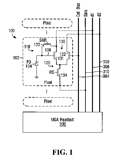
Referring to Figures 1-3, a control circuit for an image sensor according to a
first embodiment of the invention is shown generally at 100. In
this
embodiment, the control circuit 100 includes an active reset control circuit
110
configured to perform an active reset of a light flux-dependent node of a
pixel
102 of the image sensor using an amplifier 302 which is also used for readout
of the light flux-dependent node. In this embodiment, the control circuit 100
further includes a readout control circuit 120 configured to maintain a
readout
configuration of the amplifier 302 during the active reset. In this
embodiment,
the readout control circuit 120 is also configured to maintain the same
readout
configuration while performing a readout of the pixel. Also
in this
embodiment, the light flux-dependent node includes a photodetector 104, as
discussed below. The active reset control circuit 110 and readout control
circuit 120 are discussed in greater detail below in the course of elaborating
upon the pixel 102 and its operation.
IMAGE SENSOR
Referring to Figures 1-3, an image sensor including the control circuit 100 is
shown generally at 200 in Figure 2. In this embodiment, the image sensor
200 includes a Complementary Metal Oxide Semiconductor (CMOS) image
sensor. More particularly, in this embodiment the CMOS image sensor is
embodied in a chip 202 which includes a plurality of pixels, each of the
pixels
being identical to the pixel 102 shown in Figure 1 and thus including the
control circuit 100. More particularly still, in this embodiment the image
sensor 200 includes a pixels array 204 having 100 rows x 100 columns of
CA 03025801 2018-11-28
WO 2016/191852
PCT/CA2016/000162
-9-
pixels, with each of the 10,000 pixels being identical to the pixel 102.
Alternatively, other sizes of pixel arrays may be substituted.
In this embodiment, the pixels of the array 204 are controlled via a Row
Decoder and Row Logic block 210. In this embodiment, pixel control signals
are input to the Row Logic, where they are leveled up and delivered to each of
the pixel row drivers. In this embodiment, the current command is AND-ed
with a row address from the Row Decoder, in order to assert the desired
operation to the selected pixel row. In this embodiment, only two control
lines
are used to control the pixels array 204, one line for active reset and the
other
line for readout.
In this embodiment, the image sensor 200 further includes a readout block
300 and a column charge amplifiers block 400. More particularly, in this
embodiment the readout block 300 includes a Unity Gain Amplification (UGA)
readout block in communication with the pixels array 204, through which the
pixel levels of the various pixels are sampled. The column charge amplifiers
block 400 then amplifies the pixel signals according to a selected gain level.
In this embodiment, the image sensor 200 further includes an analog-to-digital
conversion (ADC) block 500. More particularly, in this embodiment the ADC
block 500 includes a single slope (SS) ADC block with 10-bit resolution, which
performs the analog-to-digital conversion in parallel for all pixels within a
given
row, and which sequentially scans digitized outputs via an out bus 502.
Also in this embodiment, the image sensor 200 includes a bias & ramp
generators block 220, which provides the required DC voltages and climbing
ramp (reference signal) for the readout block 300, the charge amplifiers block
400 and the ADC block 500. In the present embodiment, the digital control
voltages and analog bias voltages are generated off the chip 202 and relayed
to the required on-chip components by the bias & ramp generators block 220.
Alternatively, the bias & ramp generators block 220 may include an
CA 03025801 2018-11-28
WO 2016/191852
PCT/CA2016/000162
-10-
Application Specific Integrated Circuit (AS1C) configured with control code to
generate all required control signals, reference signals and biases from on-
board the chip 202.
The image sensor 200 of the present embodiment further includes a column
decoder block 230, which multiplexes the ADC triggering signals to a single
output line 232.
PIXEL
Referring to Figure 1, an illustrative one of the 10,000 pixels of the pixels
array 204 is shown at 102. In this embodiment, the pixel 102 includes the
control circuit 100, and the pixel 102 includes no more than four transistors.
More particularly, as discussed below, in this embodiment the pixel 102 has
exactly four transistors.
In this embodiment, the light flux-dependent node of the pixel 102 includes
the
photodetector 104, which detects electromagnetic radiation (light) via the
photoelectric effect, whereby photons interacting with a photoelectric
material
such as crystallized silicon cause electrons to jump from the valence band to
the conduction band. More particularly, in this embodiment the photodetector
104 is a photodiode. Alternatively, PIN photodiodes, other suitable
photodiodes or more generally other photodetectors may be substituted. In
some such embodiments, it is not the photodetector 104 itself whose signal is
to be actively reset to prevent image lag, but rather, a related pixel node
such
as a sampling node. Thus, in other embodiments, the light flux-dependent
node of the pixel, which is to be actively reset, may generally include other
pixel nodes whose measurable property (e.g. voltage) depends upon the light
flux incident upon the pixel.
In this embodiment, the readout control circuit 120 includes a differential
pair
130, which includes first and second differential pair transistors 131 and
132.
CA 03025801 2018-11-28
WO 2016/191852
PCT/CA2016/000162
-11-
In this embodiment, each of the transistors 131 and 132 is a field-effect
transistor having two channel terminals (source and drain) and a gate terminal
for controlling the flow of electrical current between the source and drain
terminals. More
particularly, in this embodiment the first and second
transistors 131 and 132 are NMOS transistors.
In this embodiment, the readout control circuit 120 further includes a readout
transistor 134 having a first channel terminal in communication with channel
terminals of the differential pair 130, and having a second channel terminal
in
communication with a shared source line. In this regard, a photosensing
node 106 at the same potential as the photodetector 104 is in electrical
communication with a gate terminal of the transistor 131. The first channel
terminal of the transistor 131 is in electrical communication with a first
load
line 306 of the amplifier 302, which in turn is connected to a drain terminal
of a
first current source transistor 331 of the amplifier 302. The second channel
terminal of the transistor 131 is in simultaneous electrical communication
with
the first channel terminal of the readout transistor 134 (which in this
embodiment includes an NMOS transistor) and with the first channel terminal
of the second differential pair transistor 132, respectively. In the present
embodiment, the second channel terminal of the readout transistor 134 is in
electrical communication with a shared source line or sink line 310 of the
readout block 300, and the gate terminal of the readout transistor 134 is in
communication with a readout signal (RS) line, one of only two digital control
lines used to control the pixel array 204 in the present embodiment. The
second channel terminal of the second differential pair transistor 132 is in
electrical communication with a second load line 308 of the amplifier 302,
which in turn is connected to a drain terminal of a second current source
transistor 332 of the amplifier 302. In this embodiment, to form a Unity Gain
Amplification (UGA) configuration, the gate terminal of the second
differential
pair transistor 132 is connected to an output line 304 of the amplifier 302 of
the readout block 300, which in this embodiment includes a column bus line.
CA 03025801 2018-11-28
WO 2016/191852
PCT/CA2016/000162
-12-
In this embodiment, the photodetector 104 and photosensing node 106 are in
electrical communication with a first channel terminal of a reset transistor
133,
which in this embodiment includes an NMOS transistor. A second channel
terminal of the reset transistor 133 is in electrical communication with the
first
load line 306 of the amplifier 302. A gate terminal of the reset transistor
133
is in electrical communication with an active reset (SAR) line, which is the
other one of the two digital control lines used to control the pixel array 204
in
the present embodiment.
As discussed in greater detail below, in this embodiment, sensing or readout
of the pixel includes pulsing the RS line to high, thereby causing the readout
transistor 134 to temporarily connect the second load line 308 to the shared
source or sink line 310.
In this embodiment, the active reset control circuit 110 includes a switching
element configured to place the light flux-dependent node in electrical
communication with an internal node of the amplifier 302 to form a negative
feedback to the light flux-dependent node. More
particularly, in this
embodiment the light flux-dependent node of the pixel 102 includes the
photodetector 104, and the switching element is configured to place the
photodetector 104 in simultaneous electrical communication with first and
second lines of the amplifier 302. To achieve this, in the present embodiment
the active reset control circuit 110 includes an asymmetrical active reset
control circuit configured to short the photodetector 104 across first and
second load lines 306 and 308 of the amplifier 302. More particularly, in this
embodiment the asymmetrical active reset control circuit includes the reset
transistor 133 to temporarily place the photodetector 104 and photosensing
node 106 in simultaneous electrical communication with both the first load
line
306 and the second load line 308 of the amplifier 302. As the load lines 306
and 308 of the amplifier 302 are not symmetrical relative to the in-pixel
differential pair 130, the present inventors have referred to this new type of
active reset as an "asymmetrical" active reset, as discussed in the Operation
CA 03025801 2018-11-28
WO 2016/191852
PCT/CA2016/000162
-13-
section below. Also
advantageously, in this embodiment the readout
configuration of the pixel 102, with the readout transistor 134 conducting
between its channel terminals, may be maintained throughout the active reset
process.
READOUT BLOCK
Referring to Figures 1-3, generally in this embodiment the readout block 300
obtains the analog levels of the various pixels of the array 204 using Active
Column Sensing (ACS).
In this embodiment, the control circuit 100, or more particularly the active
reset control circuit 110, includes the amplifier 302 of the readout block
300.
More particularly, in this embodiment the amplifier 302 is located at least
partly outside the pixel 102, and includes a folded cascode operational
amplifier (opamp). As noted above, the differential pair transistors 131 and
132 inside each pixel 102 are connected to the drain terminals of first and
second current source transistors 331 and 332 of the folded cascode
amplifier, which in this embodiment are biased by a first bias line 320 in
communication with their gate terminals and with an external bias voltage.
In this embodiment, the amplifier 302 further includes a separator circuit
350,
configured to separate the load from the rest of the amplifier 302, to boost
output impedance, and to reduce undesirable charge injections onto the load
lines 306 and 308. More particularly, in this embodiment the separator circuit
350 includes first and second cascode transistors 333 and 334, which in this
embodiment are biased by a second bias line 322 in communication with their
gate terminals and with an external bias voltage.
As noted above, the output line 304 of the amplifier 302, which in this
embodiment is the column bus line, is connected to the gate terminal of the
CA 03025801 2018-11-28
WO 2016/191852
PCT/CA2016/000162
-14-
second differential pair transistor 132 of each pixel 102, thus forming a
unity
gain amplification (UGA) configuration.
In the present embodiment, the amplifier 302 further includes biased
transistors 337 and 339, and load transistors 338 and 340. In this
embodiment, the biased transistors 337 and 339 are diode-connected and
hence self-biased, and provide the driving voltages for the load transistors
338 and 340.
In this embodiment, the amplifier 302 further includes a stability
compensation
circuit 360. In this regard, as is known in the art, a unity gain operational
amplifier generally requires a sufficient phase margin (PM) to maintain
stability, particularly if the opamp is to be used in closed loop or negative
feedback configurations.
Accordingly, in this embodiment the stability
compensation circuit 360 includes a lead compensation circuit, which more
particularly includes a metal oxide semiconductor (MOS) resistor 335 and a
Miller metal-insulator-metal (MIM) capacitor 336. The MOS resistor 335 has a
voltage-dependent resistance, which more particularly is a function of its
strength, threshold voltage and gate source voltage drop. In this embodiment,
the source and gate voltages of the MOS resistor 335 are derived from the
source and gate terminals of the diode-connected, self-biased transistor 337,
so that the overdrive voltage (gate source voltage drop minus threshold
voltage) of the MOS resistor 335 equals that of the transistor 337, thereby
ensuring a close match between the trans-conductance of the transistor 337
and the resistance of the MOS resistor 335. Advantageously, therefore, in
this embodiment the amplifier 302 achieves a remarkable phase margin (PM)
without the need for external biasing of the MOS resistor 335.
In this embodiment, the amplifier 302 further includes a current source 370,
which in this embodiment is configured to provide noise immunity for active
column sensing. More particularly, in this embodiment the current source 370
includes a cascoded current source, implemented by transistors 341 and 342.
CA 03025801 2018-11-28
WO 2016/191852
PCT/CA2016/000162
-15-
In this embodiment, the cascoded current source 370 sinks, through the Sink
line 310, the tail currents from the in-pixel differential pair transistors
131 and
132. A bias line (Bias_N) 343 sets the current through the transistor 342, and
a boost line (Cas_N) 344 sets the resistance boost of the transistor 341.
When a certain pixel has to be read out, the gate of the in-pixel readout
transistor 134 is pulsed high, connecting the pixel source to the Sink line
310,
thus activating the folded cascode structure. After a short settling time, the
pixel output appears on the output (Col_Bus) line 304 of the readout block
300, through which it is wired to the charge amplifiers block 400, where it is
boosted before the ND conversion.
In this embodiment, the transistors 331, 332, 333 and 334 are PMOS
transistors, the MOS resistor 335 includes an NMOS transistor, and the
transistors 337 to 342 are NMOS transistors.
CHARGE AMPLIFIERS
Referring to Figures 2 and 4, the charge amplifiers block is shown generally
at
400 in Figure 4. In this embodiment, the amplifier output line 304 of the
readout block 300 is connected through a sample switch 402 to a first plate of
a capacitor 404. In this embodiment, the capacitor 404 has a capacitance of
100 fF, and a second plate of the capacitor 404 is grounded. Generally, in
this embodiment the capacitor 404 and other capacitors of the charge
amplifiers block 400 are Metal-Insulator-Metal (MI M) capacitors.
In this embodiment, the first plate of the capacitor 404 is connected to a
first
selector circuit shown generally at 405, which in this embodiment includes a
main sampling capacitor 406, a first switch 408, a bypass sampling capacitor
410 and a second switch 412. In this embodiment, the main sampling
capacitor 406 has a capacitance of 2.5 pF, while the bypass sampling
capacitor has a capacitance of 100 fF.
CA 03025801 2018-11-28
WO 2016/191852
PCT/CA2016/000162
-16-
In the present embodiment, an output node 414 of the first selector circuit
405
is connected to an amplifier, which in this embodiment includes an operational
transconductance amplifier (OTA) 416. More particularly, in this embodiment
the output node 414 of the first selector circuit 405 is connected to the
inverting (-) input of the OTA 416, while a non-inverting (+) input 418 of the
OTA 416 is connected to a common mode (CM) or reference line.
In this embodiment, an output line 420 of the OTA 416 is in electrical
communication with a second selector circuit 422. In this embodiment, the
second selector circuit 422 includes four different feedback capacitors 424,
426, 428 and 430, selectable through actuation of respective switches 432,
434, 436 and 438. In this embodiment, the capacitances of the feedback
capacitors 424, 426, 428 and 430 are 100 fF, 50 fF, 25 fF and 5 fF,
respectively, and the switches 432, 434, 436 and 438 are actuatable by
raising or lowering corresponding independent gate terminal gain signals
G_25, G_50, G_100 and G_500.
In this embodiment, to achieve gain values greater than unity, a Bypass signal
is kept low to maintain the second switch 412 in an open (non-conducting)
state, while a Bypass_b signal is set high to close the first switch 408,
thereby
connecting the pixel's column bus output signals on the readout block's output
line 304 to the main sampling capacitor 406. One of the gain signals G_25,
G _ 50, G_100 or G_500 is raised, in order to select a respective gain level
of
25, 50, 100 or 500, corresponding to a respective one of the feedback
capacitors 424, 426, 428 and 430.
Alternatively, if a unity gain is desired, the Bypass and Bypass_b signals may
be inverted, to open the first switch 408 and close the second switch 412,
thereby connecting the pixel's column bus output signals on the readout
block's output line 304 to the bypass sampling capacitor 410. In this
embodiment, the capacitance of the bypass sampling capacitor 410 is only
100 fF, or 1125th that of the main sampling capacitor 406. Accordingly, to
CA 03025801 2018-11-28
WO 2016/191852
PCT/CA2016/000162
-17-
achieve unity gain, the G_25 signal is set high while the G_50, G_100 and
G_500 signals are kept low, thereby selecting a gain of 25 corresponding to
the feedback capacitor 424. The selected 25x gain offsets the 25x reduction
that resulted from substituting the bypass sampling capacitor 410 for the main
sampling capacitor 406, resulting in a gain of 1.
As a further alternative, if desired, all of the feedback switches may be
simultaneously activated, resulting in a gain of 0.5, which may be suitable
for
some wide dynamic range (WDR) capture applications. More particularly, in
this embodiment a gain of 0.5 may be achieved by: setting the Bypass signal
high to close the switch 412 to select the bypass sampling capacitor 410;
setting the Bypass_b signal low to open the switch 408 to thereby de-select
and bypass the main sampling capacitor 406; setting the Reset_A signal low
to open the switch 440 and setting all of the G_25, G_50, G_100 and G_500
signals high to close all of the gain switches 432, 434, 436 and 438 to
simultaneously select all four of the feedback capacitors 424, 426, 428 and
430.
In this embodiment, the charge amplifiers block 400 further includes a reset
switch 440 for resetting the charge amplifier, as discussed in greater detail
below.
Thus, the present embodiment employs single phase amplification, i.e.,
amplification in which the charge integration and charge transfer occur
concurrently, rather than two-phase amplification, in which the charge
integration and transfer are separate operations. Two-phase amplification
typically requires additional switching hardware to switch the positive
sampling capacitance terminal between the input and the common mode or
reference level CM, which may also decrease the signal integrity.
Advantageously, therefore, the present embodiment avoids these difficulties.
Alternatively, however, other embodiments may employ two-phase charge
amplifiers, or more generally other types of charge amplifiers.
CA 03025801 2018-11-28
WO 2016/191852
PCT/CA2016/000162
-18-
ANALOG-TO-DIGITAL CONVERSION
Referring to Figures 2, 5 and 6, the ADC block is shown generally at 500. In
this embodiment, the ADC block 500 includes a comparator circuit shown
generally at 510, and a register circuit shown generally at 600.
For the comparator to have sufficient gain and speed, in this embodiment the
comparator circuit 510 has a two-stage configuration, based upon a
differential amplifier. A single stage amplifier, when driven through very low
impedance, can be regarded as a single pole system, and therefore maintains
a phase margin (PM) of 90 under a closed loop configuration. Therefore, the
chosen topology allows not only for a remarkable gain, but for a simple offset
compensation, when the offset of each stage is mitigated by closing a loop
around a differential amplifier. Offset compensation is discussed in greater
detail below under the heading, "Operation".
Accordingly, in this embodiment the comparator circuit 510 includes first and
second differential amplifiers 520 and 530. The input signal to the comparator
circuit 510 is the signal from the output line 420 of the column charge
amplifier
400 shown in Figure 4. Through a first switch 512, the input signal from the
output line 420 is connected to the first plate of a capacitor 514, which is
also
connected through a second switch 516 to a reference Ramp voltage. In this
embodiment, the reference Ramp voltage is generated as a single
continuous, monotonically increasing signal, thereby avoiding the need for the
additional circuitry required for a step-wise reference generator.
In this embodiment, a second plate of the capacitor 514 is in electrical
communication with an inverting (-) input of the first differential amplifier
520.
The output of the first differential amplifier 520 is in communication with a
first
plate of a capacitor 524. In addition, through actuation of a switch 522, the
output of the first differential amplifier 520 may be also placed into and out
of
CA 03025801 2018-11-28
WO 2016/191852
PCT/CA2016/000162
-19-
electrical communication with its own inverting input, effectively closing a
loop
around the first differential amplifier 520.
Similarly, in this embodiment a second plate of the capacitor 524 is in
electrical communication with an inverting (-) input of the second
differential
amplifier 530. The output of the second differential amplifier 530 is in
communication with a step-down level shifter 540, which provides a digital
domain trigger signal Trig<i> as discussed in greater detail below. In
addition,
through actuation of a switch 532, the output of the second differential
amplifier 530 may be also placed into and out of electrical communication with
its own inverting input (-), effectively closing a loop around the second
differential amplifier 530.
In this embodiment, the non-inverting input (+) of the second differential
amplifier 530 is in electrical communication via a switch 534 with the output
line 420 of the column charge amplifier to receive its input signal therefrom,
and is also in electrical communication via a switch 536 with the reference
Ramp signal discussed earlier herein.
In this embodiment, the register circuit 600 includes a 10-bit register with
parallel loading and serial scanning / unloading. More particularly, in this
embodiment the register circuit 600 includes a 10-bits counter 602, which in
this embodiment is synchronized with a clock signal CLK received on a clock
line 604. In this embodiment, the register circuit 600 is also in
communication
with the step-down level shifter 540 which provides the digital trigger signal
Trig<i>. When the latter trigger signal is received, it causes latching of the
code generated by the 10-bits counter 602 into a column-wise 10-bit register
606. As discussed below, in successive cycles, the contents of the column-
wise 10-bit register 606 are shifted one position to the right through
successive column registers shown generally at 608, toward the output line
502 of the ADC block 500.
CA 03025801 2018-11-28
WO 2016/191852
PCT/CA2016/000162
-20-
In this embodiment, the digitized output stream from the output line 502 is
supplied to an off-chip Field Programmable Gate Array (not shown), from
which it is transferred to a display screen.
In this embodiment, the column decoder 230 shown in Figure 2 is also
employed. The column decoder 230 effectively serves as a backup for the
digital memory (counter and registers) of the register circuit 600, by
multiplexing the various ADC signals onto a single output line 232, thus
permitting the analog pixel output signals to be independently digitized off
the
chip 202 to obtain the final image. Alternatively, the column decoder 230 may
be omitted if desired.
OPERATION
In this embodiment, to capture an image frame from the image sensor 200, a
first row of pixels of the pixels array 204 is selected and addressed via the
row
decoder and row logic block 210.
Next, the charge amplifiers block 400 is placed in a pixel-sampling
configuration, while an active reset is performed at each pixel 102 of the
currently selected pixel row, thereby establishing an initial DC level of the
output 304 of the readout block 300.
To achieve the pixel-sampling configuration of the charge amplifiers block
400, a Sample signal that controls the sample switch 402 is pulsed high,
thereby closing the switch 402 and placing the output line 304 (col. bus) of
the
readout block 300 in communication with the OTA 416 via the first selector
circuit 405.
In this embodiment, the active reset of the currently addressed pixel row
involves performing an active reset of the photodetector 104 of each pixel 102
of the currently selected pixel row of the image sensor 200 using the
amplifier
CA 03025801 2018-11-28
WO 2016/191852
PCT/CA2016/000162
-21-
302 which is also used for readout of the photodetector 104. Advantageously,
in this embodiment a readout configuration of the amplifier 302 is maintained
during the active reset.
In this embodiment, performing the active reset includes performing an
asymmetrical active reset, which in this embodiment includes shorting the
photodetector 104 across the amplifier 302. More
particularly, in this
embodiment shorting includes placing a photosensing element of the
photodetector 104 or the photosensing node 106 of the photodetector 104 in
simultaneous electrical communication with the first and second load lines
306 and 308 of the amplifier 302. In this embodiment, this is achieved by
setting the active reset (SAR) signal received at the gate terminal of the
reset
transistor 133 high, thereby placing the photodetector 104 and its
photosensing node 106 in simultaneous electrical communication with the
both of the load lines 306 and 308 of the amplifier 302. Advantageously,
therefore, in this embodiment the active reset is controlled using just a
single,
in-pixel reset transistor 133.
As noted above, in this embodiment the readout control circuit 120
advantageously maintains the readout configuration of the amplifier 302
during the active reset. In this embodiment, it will be recalled that the
output
line 304 of the amplifier 302 is connected to the gate terminal of the second
in-pixel transistor 132, thereby forming a unity gain configuration of the
amplifier 302. Thus, in this embodiment maintaining the readout configuration
of the amplifier 302 during the active reset includes maintaining a unity gain
configuration of the amplifier 302. More particularly, in this embodiment
maintaining the unity gain configuration includes maintaining the output 304
of
the amplifier 302 in electrical communication with the gate terminal of a
switching element (in this case the second differential pair transistor 132),
wherein the switching element has a source terminal in electrical
communication with a current source load line (in this case the second load
line 308) of the amplifier 302. More particularly still, in this embodiment
the
CA 03025801 2018-11-28
WO 2016/191852
PCT/CA2016/000162
-22-
readout control circuit 120 includes the differential pair 130. One of the
differential pair (the transistor 132) includes the switching element. The
other
of the differential pair (the transistor 131) has a gate terminal in
electrical
communication with the light flux-dependent node (in this embodiment the
photodetector 104), and has a channel terminal in electrical communication
with a second load line of the amplifier 302.
In this embodiment, in order to maintain the readout configuration of the
amplifier 302 during the active reset, simultaneously with setting the active
reset (SAR) signal high, the readout (RS) signal received at the gate terminal
of the readout transistor 134 is also pulsed high, thereby placing the sink
line
310 of the current source 370 in electrical communication with the second
load line 308 of the amplifier 302.
Thus, during the asymmetrical active reset of the present embodiment, two
closed loops exist simultaneously: a readout loop, and an active reset loop
formed by activation of the reset transistor 133. In this embodiment, the
reset
voltage is set by the DC operating point of the formed active reset loop. As
noted earlier, in this embodiment the active reset is controlled using only
the
reset transistor 133. Advantageously, this permits a reduction of both in-
pixel
and column-shared circuitry, as discussed earlier herein.
Referring to Figures 1 and 3, in this embodiment, with the transistors 133 and
134 both in their conducting states during the active reset, some current will
flow from the transistor 331 of the amplifier 302, through the first load line
306,
to the photodetector 104 and photosensing node 106, effectively charging the
photodetector 104. Due to the maintained unity gain readout configuration of
the amplifier 302, the output 304 of the readout block 300 (and hence the gate
of the second in-pixel differential pair transistor 132) will closely follow
the
level of the photodetector 104 from this moment onward.
CA 03025801 2018-11-28
WO 2016/191852
PCT/CA2016/000162
-23-
Referring to Figures 1-4, in this embodiment, as soon as the initial DC level
of
the output 304 of the amplifier has been established in the above manner, the
column charge amplifiers block 400 is also reset. To achieve this, in this
embodiment the reset signal (Reset_A) received at the reset switch 440 of the
column charge amplifiers block 400 is pulsed high, thereby closing the switch
440 and thus placing the output 420 of the OTA 416 in electrical
communication with the node 414 to which the inverting (-) input of the OTA
416 is connected. Consequently, node 414 converges to the common mode
(CM) reference level which is supplied to the non-inverting (+) input of the
OTA 416. It will be recalled that the Sample signal received at the switch 402
is still high so that the switch 402 is closed, and likewise one of the
switches
408 and 412 will also be closed depending on whether the Bypass or
Bypass_b signal is high. Consequently, closing the reset switch 440 and
causing the node 414 to converge to the common mode reference level CM
resets the input capacitance CgH of the capacitor 404, as well as either the
input capacitance CIN of the main sampling capacitor 406 or the input
capacitance Cgp of the bypass sampling capacitor 410, depending on which of
the switches 408 and 412 is closed.
In this embodiment, the active reset (SAR) signal supplied to the reset
transistor 133 of the pixel 102 is then set low, and shortly thereafter, the
Reset_A signal supplied to the switch 440 of the column charge amplifiers
block 400 is also set low, causing the switch 440 to open. This enables the
incoming pixel signal received on the output line 304 of the readout block 300
to be amplified with a gain equal to the ratio of the input capacitance to the
feedback capacitance, where the input capacitance is determined by which of
the switches 408 and 412 of the first selector circuit 405 is closed, and the
feedback capacitance is determined by which one or more of the capacitors
424, 426, 428 and 430 has been selected by closing its respective gain switch
432, 434, 436 or 438.
CA 03025801 2018-11-28
WO 2016/191852
PCT/CA2016/000162
-24-
Next, when it is time to obtain a digital sample of the pixel signal, in this
embodiment the Sample signal received at the switch 402 of the column
charge amplifiers block 400 is pulsed low, thereby opening the switch 402 and
temporarily disconnecting the column charge amplifiers block 400 from the
output 304 of the readout block 300. This latches the final pixel level on the
capacitor 404, and thus maintains the output 420 constant for the subsequent
analog-to-digital conversion.
Referring to Figure 5 and 6, in this embodiment the analog-to-digital
converter
500, or more particularly the comparator 510, performs offset cancellation, by
closing a loop around a differential amplifier in order to mitigate the offset
of
each comparator stage. More particularly, in the present embodiment the
offset cancellation is divided into three distinct phases. First, the signal
Convert supplied to the switches 512 and 534 is set low and the signal AZ_3
supplied to the switches 516 and 536 is set high, thereby closing the switches
516 and 536 and connecting the reference Ramp voltage, which is constant at
that moment, to a positive terminal of the capacitor 514, and to the non-
inverting (+) input of the second stage amplifier 530. Second, the signals
AZ_1 and AZ_2 supplied to the switches 522 and 532 are set high, to store
the comparators' offsets on the Caz1 and Caz2 capacitors 514 and 524,
respectively, respectively. Next, the AZ_1 signal supplied to the switch 522
is
pulsed low, while the AZ_2 signal supplied to the switch 532 is still high,
thereby storing on the capacitor 524 the offset caused by the charge
injections from the first stage loop disconnection. Finally, the AZ_2 and AZ_3
signals supplied to the switches 516, 532 and 536 are set low, while the
Convert signal supplied to the switches 512 and 534 is set high, preparing the
two stage comparator for the subsequent conversion.
As noted earlier, in this embodiment the reference Ramp signal is generated
as a single continuous, monotonically increasing signal. More particularly, in
this embodiment the reference Ramp signal is initially maintained constant
during offset cancellations, and thereafter starts climbing, spanning the
CA 03025801 2018-11-28
WO 2016/191852
PCT/CA2016/000162
-25-
amplified pixel level found on the output line 420 of the column charge
amplifier which is in communication with the input switches 512 and 534 of the
comparator 510. In this embodiment, as the reference Ramp signal value
crosses the amplified pixel value, the two stages' comparator toggles and
generates a negative pulse, which the step down level shifter 540 inverts and
adjusts to generate a digital domain trigger signal Trig<i>. This digital
domain
trigger signal Trig<i> is received at the register circuit 600, and enables
the
latching of the code generated by the 10 bits counter 602 into the column-
wise 10 bit register 606. In this regard, in the present embodiment, the code
generation within the 10 bits counter 602 is synchronized to a clock signal
CLK, and thus the 10 bits counter 602 directly measures elapsed time. The
time required for the voltage of the reference Ramp signal to rise to the
voltage of the pixel signal present on the output line 420, and thus cause the
comparator circuit 510 to generate the Trig<i> signal, is proportional to the
voltage of the pixel signal present on the output line 420. Thus, in this
embodiment the 10 bit time value that is latched from the 10 bits counter 602
to the column-wise 10-bit register 606 in response to the Trig<i> trigger
signal
effectively represents an indirect digital measurement of the analog pixel
signal voltage present on the output line 420.
Accordingly, in this
embodiment, the 10 bits counter 602 begins to count elapsed time values. In
response to the Trig<i> trigger signal generated at the step-down level
shifter
540, the 10-bit code currently stored in the 10 bits counter 602 is latched
into
the column-wise 10-bit register 606. The counter 602 continues to count until
the end of its 10-bit counting cycle (210 time increments from 0 to 1023), at
which time the contents of the column-wide 10-bit register 606 and the current
contents of the other column registers 608 are shifted one position toward the
right in Figure 6 toward the output bus 502. In the present embodiment, for
parallel loading of a digital word, the signal Read is low, whereas its
complementary phase Read_b is high. As the conversion is due, the phases
are inverted forming a 10 bit shift register for the sequential scan of the
digitized pixel values. Every counting cycle, the contents of each column
CA 03025801 2018-11-28
WO 2016/191852
PCT/CA2016/000162
-26-
register are shifted right towards the output bus 502, which effectively
outputs
a digital stream of column register data.
In this embodiment, the above steps are repeated as needed to obtain digital
pixel data for the remaining pixels of the currently selected pixel row, and
then
for the pixels of all other pixels of the array 204 for each frame, and are
likewise repeated to obtain successive frames. In this embodiment, the digital
output stream on the output bus 502 is received at an off-chip Field
Programmable Gate Array (FPGA) (not shown), which re-organizes the digital
output stream and controls a video display device (not shown) to display the
images represented by the digital output stream.
PROTOTYPE PIXEL AND SIMULATIONS
Referring to Figures 1 and 7, a prototype of the pixel 102 is shown generally
at 700 in Figure 7. The pixel 700 was implemented in TSMC018 1poly, 6
metals technology. The resulting pixel pitch was 10 pm with a photodiode PD
area (Fill Factor) of 40%. To facilitate a proper operation, the analog lines,
namely Col_Bus, d2, Sink, and dl (corresponding to lines 304, 308, 310 and
306 respectively in Figure 1) were laid perpendicularly to the digital lines
SAR
and RS (which respectively connect to the reset transistor 133 and the
readout transistor 134 in Figure 1). Furthermore, lines dl and d2,
implemented in the same metal, were placed on opposite sides of the shared
source line Sink, achieving a better common noise rejection and an extended
decoupling one from another. The other two analog lines were implemented in
a different metal to minimize the coupling between the four lines.
The present inventors have also generated simulations of circuits similar to
those discussed above, using CadenceTM circuit simulation software available
from Cadence Design Systems, Inc. of San Jose, CA, USA.
CA 03025801 2018-11-28
WO 2016/191852
PCT/CA2016/000162
-27-
For example, referring to Figure 8, it can be readily seen that the active
reset
has significantly decreased the KTC or reset noise: the initially injected
input
noise 802 appears to be roughly five times greater than the resulting
simulated output noise 804.
A simulation also showed that, following commencement of the active reset by
setting the SAR signal high, once a self-biased reset level around 2.2V had
been set, the pixel output on the Col_Bus output line 304 closely followed the
discharge of the photodetector 104, with the difference between the two
signals remaining under 20 pV across a wide voltage swing from 2.2V to 1.1V.
Below 1.1V the folded cascode amplifier 302 leaves its saturation region,
causing the output line 304 to diverge from the photodetector 104. The
readout precision achieved in the simulation allows for detection of a single
electron, which substantially surpasses the sensitivity of a conventional
source follower.
ALTERNATIVES:
Referring to Figures 1, 9 and 10, a pixel according to a second embodiment of
the invention is shown generally at 900 in Figure 9. The pixel 900 is similar
in
some ways to the pixel 102: for example, like the pixel 102, in this
embodiment
the pixel 900 also includes an active reset control circuit 902 configured to
perform an active reset of a light flux-dependent node (specifically the
photodetector 104) of the pixel 900 using an amplifier 1000 which is also used
for readout of the photodetector 104, and further includes a readout control
circuit 904 configured to maintain a readout configuration of the amplifier
1000
during the active reset. Thus, in this embodiment the active reset control
circuit
902 includes the reset transistor 133 of the pixel 102, and the readout
control
circuit 904 includes the readout transistor 134 and the differential pair
transistor
131 of the pixel 102, although the location of the readout transistor 134 is
changed in the pixel 900.
CA 03025801 2018-11-28
WO 2016/191852
PCT/CA2016/000162
-28-
In this embodiment, however, the pixel 900 has been considerably simplified.
The second transistor 132 of the differential pair 130 has been removed from
the pixel 900, effectively moving it to the column periphery as discussed
below.
In view of this change, corresponding changes have been made to the readout
amplifier 1000. Previously, the readout transistor 134 of the pixel 102
separated
the differential pair 130 comprising both transistors 131 and 132 from the
sink
line 310. In the pixel 900, however, the readout transistor 134 separates only
the transistor 131 from the sink line. Consequently, to maintain a similar
signal
path, in this embodiment a switch is added at the column periphery to equalize
the voltage drop in the complementary branches of the readout amplifier.
Thus, referring to Figures 3 and 10, in this embodiment the amplifier 1000
differs
from the amplifier 302, insofar as transistors 1002 and 1004 have been added.
Transistor 1002 effectively completes the differential pair to replace the
removed
transistor 132, while transistor 1004 compensates for the above-noted voltage
drop.
Accordingly, in this embodiment the readout control circuit 120 includes a
first
transistor (in this case the transistor 131) having a gate terminal in
electrical
communication with the light flux-dependent node (which in this embodiment
includes the photodetector 104) and having a first channel terminal in
electrical
communication with the first load line 306 of the amplifier 302, and a readout
transistor (in this case the transistor 134) configured to conduct between a
second channel terminal of the first transistor 131 and a sink line 310 of the
amplifier 302 in response to a readout signal received at a gate terminal of
the
readout transistor 134.
Also in this embodiment, the active reset control circuit 110 includes the
reset
transistor 133, which in this embodiment is configured to place the light flux-
dependent node (in this embodiment the photodetector 104) in simultaneous
electrical communication with a sink line and a load line of the amplifier.
More
generally, in this embodiment the pixel 900 consists essentially of the three
CA 03025801 2018-11-28
WO 2016/191852
PCT/CA2016/000162
-29-
transistors 131, 133 and 134 plus the photodetector 104. Not only has the
transistor 132 been removed from the pixel, but two bias lines (the output
line
Col. Bus. And the load line d2) have also been removed. The reset transistor
is
configured slightly differently than in Figure 1, to form the reset loop by
simultaneously connecting the photodetector 104 to the sink line 310 and the
first load line 306, rather than shorting it across both load lines 306 and
308.
Advantageously, therefore, the present embodiment provides active reset in a
"3T" pixel having only three transistors and two bias lines (Sink and dl).
Consequently, the fill factor of the pixel 900 is considerably higher than
that of
the pixel 102. More particularly, in embodiments of the pixel 900 it is
expected
that a fill factor (FF) in excess of 75% can be achieved with careful
packaging.
Although the embodiments described above employed unity gain amplification
(UGA) in the readout block 300, alternatively, embodiments of the present
invention may be employed in single ended or in open loop readout schemes,
for example. By using in-pixel amplification, higher sensitivity can be
achieved
while at the same time reducing the column processing circuitry.
For example, referring to Figures 1 and 11, a modified "4T" (four-transistor)
pixel
employing a single ended open loop amplification scheme is shown generally at
1100 in Figure 11. To modify the pixel 102 to form the pixel 1100, instead of
closing a readout loop through an amplifier output line Col_Bus, a common
reference signal (Ref) line 1102 is provided and is placed in electrical
communication with the gate terminal of the transistor 132, and the amplified
signal Out is obtained from the column shared load line.
Similarly, referring to Figures 9, 10, and 12, the "3T" pixel 902 of Figure 9
may
similarly be modified for non-unity gain readout to form a pixel 1200
employing a
single ended open loop amplification scheme. In
this embodiment, the
transistors 1002 and 1004, found within the column shared amplifier Col_Amp,
complete the differential pair, resembling the configuration of Figure 10. The
output Out_O provides the amplified signal.
CA 03025801 2018-11-28
WO 2016/191852
PCT/CA2016/000162
-30-
Referring to Figures 9 and 13, a multi-stage amplification scheme is shown
generally at 1300 in Figure 13. In this embodiment, a modified 3T pixel 1310
similar to the pixel 902 is shown in conjunction with a two-stage amplifier,
which
in this embodiment includes a column preamplifier and active reset stage 1320,
and a second amplifying stage 1330.
Referring to Figures 14 and 15, two illustrative Wide Dynamic Range (WDR)
configurations are respectively shown at 1400 in Figure 14 and at 1500 in
Figure
15.
In the first WDR configuration 1400 shown in Figure 14, a typical WDR
implementation is applied to a novel 4T pixel 1502 similar to the pixel 102,
whereby the pixel is sampled through Active Column Sensing throughout the
integration, and the pixel level Out signal is then fed to a Comparator 1504.
The
comparator 1504 is paired with Reset Logic 1506 to generate the next WDR bit,
which is written into a memory 1508.
In the second WDR configuration 1500 shown in Figure 15, a ranging procedure
is employed, whereby the pixel 1502 is allowed to integrate for a short period
of
time to assess the light intensity it receives before the main integration
starts.
To achieve this, in this embodiment a charge amplifier 1552 is inserted
between
the pixel out signal and the comparator 1504. This way, the WDR extension bits
are set prior to the main integration and the pixel is reset according to the
information stored inside the Memory 1508, advantageously omitting multiple
write memory operations that would have been required with the more typical
WDR implementation discussed in connection with Figure 14.
In this embodiment, the charge amplifier 1552 is similar to the column charge
amplifiers block 400 shown in Figure 4, apart from the feedback capacitors,
which have to be scaled differently than the feedback capacitors 432, 434, 436
and 438 of Figure 4. More particularly, the feedback capacitors of the charge
CA 03025801 2018-11-28
WO 2016/191852
PCT/CA2016/000162
-31-
amplifier 1552 are scaled according to the 0.5' ratio to the input
capacitance, i.e.
0.5, 0.25, 0.125, etc., resulting in 2i amplification. In this embodiment,
after the
pixel finishes the short integration, its signal is amplified by gradually
increasing
gains and is compared to the threshold voltage of the comparator 1504. Upon
crossing it, for the first time the WDR information is generated and written
into
the memory 1508.
Further variations of the second WDR configuration 1550 are also
contemplated. For example, the threshold can be varied, leaving the gain
constant. Alternatively, the gains and the threshold can be varied in a
certain
sequence to decrease the Threshold voltage precision requirements, for
example.
Although the embodiments described above have pertained to active reset of a
photodetector, alternatively, the improved active reset methods described
herein
may alternatively be applied to any other light flux-dependent node of the
pixel,
i.e. a node whose measurable property (such as voltage for example) depends
upon the light flux received at the pixel, such as a sampling node, for
example.
Similarly, although the embodiments above involved placing the photodetector
in simultaneous electrical communication with first and second lines of
specific
amplifiers, more generally the photodetector (or other pixel node to be
actively
reset) may be actively reset using any internal amplifier node(s) that can
form a
negative feedback to the photodetector (or other pixel node).
Similarly, although the embodiments described above have involved measuring
the photodetector's voltage and using feedback to actively reset the
photodetector's voltage, alternatively, other embodiments may involve
measuring other light-dependent properties, such as current.
In addition to the embodiments described above, it is contemplated that any
one
or more features of any particular embodiment may be combined with any one
CA 03025801 2018-11-28
WO 2016/191852
PCT/CA2016/000162
-32-
or more features of any other embodiment, except where such features have
been described as mutually exclusive alternatives.
More generally, while specific embodiments of the invention have been
described and illustrated, such embodiments should be considered illustrative
of
the invention only and not as limiting the invention as defined by the
accompanying claims.