Note: Descriptions are shown in the official language in which they were submitted.
ELECTRONIC CIRCUIT FOR CONTROL OR COUPLING OF SINGLE CHARGES OR
SPINS AND METHODS THEREFOR
[001] This application claims priority to US provisional patent application
serial number
62/347,346 filed 8 June 2016.
Technical Field
[002] This invention relates to quantum computing, and in particular to a
micro-electronic
circuit for control or coupling of single charges or spins, quantum computing
systems
incorporating the circuit and methods therefor.
Background
[003] In quantum computing, there is a need for means for controlling and
coupling of single
charges and spins.
[004] In accordance with one approach for the encoding and manipulation of
quantum
information, what is required is confinement of single electrons. The spin
degree of freedom of
the electron provides a natural two-level quantum system to encode the
information in the form of
a quantum bit (qubit), the fundamental unit of quantum information. In this
case, the qubit includes
a spin up state (state 0), a spin down state (state 1), and interim states
that are a superposition of
both the spin up and spin down states at the same time. The states of a qubit
can be represented as
points on the surface of a sphere (the Bloch sphere), as depicted in Figure 1.
[005] Of the variety of approaches to confining electron spins, confinement
of a single
electron spin in solid-state is sought with the goal of integration with solid-
state (micro-)
electronics. Quantum Dots (QDs) provide such confinement by using, in some
implementations,
electric control gates on a semiconductor substrate. Frequently used
substrates include silicon (Si),
aluminum gallium arsenide heterostructures (AlGaAs/GaAs), silicon germanium
heterostructures
(Si/SiGe), and indium arsenide (InAs).
Quantum computation with spin qubits in quantum dots
[006] Quantum computation is generally represented as a sequence of
operations requiring
precise functionalities from a physical circuit. A typical sequence is
represented in Figure 2 for a
circuit constituted of single electron spin qubits with quantum dots.
1
Date Recue/Date Received 2023-09-11
[007] What is required first is an array of quantum dots (QDs) and, in some
implementations,
their reservoir (R), like in Figure 2a. Then each quantum dot is initialized
with one electron from
its reservoir, as illustrated in Figure 2b. A means for detecting the charge
occupation of the QD is
thus necessary. This is usually achieved by counting electrons with proximal
charge sensors, e.g.
quantum point contacts, single electron transistors (SET), or capacitively
coupled electrodes.
[008] The next requirement is the ability to initialize all the qubits to a
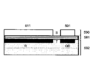
known state. It is
performed in some implementations by applying an external magnetic field to
polarize the spins,
as depicted in Figure 2c.
[009] Once spins are initialized, the actual computation can begin. A
computation can be
executed by an adequate combination of single spin rotations (R) and exchange
coupling between
neighboring spins (J) (Figure 2f). Arbitrary single spin rotations are
generally realized with the
application of electron spin resonance (ESR) pulses (Figure 2d). Being a very
short range
interaction, the exchange coupling is turned on and off by modulating the
tunnel barrier between
adjacent quantum dots (Figure 2e).
[0010] Finally, the ability to readout some or preferably all of the qubits
is necessary to
determine the result of a quantum calculation. In some implementations, this
can be obtained by
spin dependant tunneling to the reservoir, where the electron occupation in
the dot remains one if
the spin is up, and becomes zero if the spin is down. The change in occupation
is detected by
charge sensing (Figure 2g).
[0011] In some attempts, control of coherent electron spin states in
quantum dots is limited by
short coherence times (very short stability of the superposition state). In
this sense qubits are very
fragile entities. The challenge is to protect the state of a qubit from the
surrounding environment
long enough to achieve a sufficient number of logic operations on the quantum
state for useful
calculations. In order to achieve this feat, the surrounding environment has
to be controlled to the
fullest extent possible. It has been demonstrated that isotopically enriched
'Si substrates offers
sufficiently long coherence times for robust quantum computing with spin
qubits in quantum dots.
Quantum dots
2
Date Recue/Date Received 2023-09-11
[0012] Many architectures for quantum dots have been proposed. Prior art comes
in two forms:
arena designs and local accumulation designs. Both forms have been successful
in demonstrating
several functionalities necessary to quantum computation.
[0013] Arena designs rely on electrostatic gates to deplete regions of a
two-dimensional
electron gas (2DEG), formed by a heterostructure and/or by a global
accumulation gate. Figure 3A
is a typical implementation published in the literature. The electrostatic
gates (dashed structures)
define two quantum dots, QD1 and QD2, tunnel coupled to each other and to
reservoirs RI and
R2. A nearby single electron transistor (SET) formed by reservoir R3, QD3 and
reservoir R4 is
used as a charge sensor of the Double-Quantum-Dot (DQD). Barrier gates 341,
342 and 343
control the tunnel barriers between the reservoirs and the dots, represented
by the double arrows.
Barrier gates 342 and 331 control the tunnel barrier between the dots, also
represented by arrows.
Confinement gates 351 to 354 define the size of quantum dots. Plunger gates
352 and 353 set QD1
and QD2 charge states. Gate 371 sets the tunnel barriers and the charge state
of the SET. The
region labeled 2DEG represents electrons not confined by the gates. The scale
bar indicates typical
structure dimension in GaAs devices.
[0014] Figure 3B shows a cross section of the arena device in Fig 3A,
following a section
along the points A and B in Fig 3A. The 2DEG is formed in the quantum well
layer 393 of the
heterostructure 392. The depletion gates, such as 371, 351, and 354, deplete
regions of the 2DEG
to form the quantum dots QD3, QD1 and QD2. Figure 3C shows a cross section of
a device
employing a global top gate (395) to create the 2DEG. The depletion gate
layout is similar to the
one of the device in Figure 3A. A dielectric layer 394 isolates the depletion
gates such as 371, 351,
and 354, from the global top gate. Layer 391 is the gate oxide that isolates
the 2DEG from the
gates.
[0015] In local accumulation designs, dots and/or reservoirs can be
formed directly by local
accumulation gates instead of a combination of a global accumulation gate and
electrostatic gate
areas. Additional gates increase the confinement of accumulated regions and
control the tunnel
barriers. For example, in the article by Teck Seng Koh, John King Gamble, Mark
Friesen, M. A.
Eriksson, and S. N. Coppersmith titled Pulse-Gated Quantum-Dot Hybrid Qubit
published in
Physics Review Letters, PRL 109, 250503 (2012), there is disclosed a device
geometry for a top-
gated Si/SiGe heterostructure as illustrated in Figure 4A. The Koh et al.
article is also related to
3
Date Recue/Date Received 2023-09-11
US patent application publication 2015/0279981 published on October 1, 2015.
The quantum dot
well is provided using an accumulation gate, while the reservoir is provided
using a depletion
mode tunnel barrier gate and confinement in the well is enhanced using various
depletion mode
gates. Figure 4B is a further state of the art implementation published in the
literature. Two
quantum dots, QD1 and QD2, are connected in series to reservoir R2. A proximal
single electron
transistor formed by reservoir R3, QD3 and reservoir R4 is used as a charge
sensor of the double
quantum dot DQD. The quantum dots and reservoirs are defined by accumulating
electrons under
electrostatic gates 401, 402, 412, and 421. Gate 451 ensures lateral
confinement of the double
quantum dot. Gates 431, 442, 473, and 474 control tunnel barriers between
accumulated regions.
The scale bar indicates typical structure dimension in Si devices.
[0016] Figure 4C shows a cross section of the local accumulation device
in Fig 4B, following
a section along the points A and B in Fig 4B. While it is not apparent in
Figure 4A for clarity, the
different gates are stacked one on the other as depicted in Fig 4C. A thin
oxide (not shown) covers
each gate to insulate it from the others. Gates 401, 402, 412 and 421
accumulate locally the QDs
and reservoirs, while gate 451 laterally confines QD1 and QD2. Gate 431
control the tunnel barrier
between QD1 and QD2, and gate 442 controls the tunnel barrier between QD2 and
R2.
Summary
[0017] The transistor is the basis of information technology, the
elementary unit of
supercomputers predicting weather and the basis of portable computing
providing access to
knowledge to the whole world. The efficiency of transistors to process
information resides in their
integration by the millions into integrated circuits enabled by Complementary
Metal-Oxide-
Semiconductor (CMOS) technology, a class of integrated circuits. CMOS
technology has enabled
the era of information technology. The present invention facilitates a second
information
technology revolution using CMOS, by simplifying information processing in a
quantum
computer. Quantum computing seeks to exploit the properties unique to "the
world of the very
small" to solve complex problems. But the full potential of quantum computers
has not been yet
imagined.
[0018] Spin qubits in quantum dots are a promising platform for quantum
information
processing. The present invention allows to simplify the implementation and
control of spin qubits
4
Date Recue/Date Received 2023-09-11
in a scalable fashion using CMOS compatible technology, thus harnessing the
full potential of the
semiconductor industry for large scale integration and manufacturing.
[0019] It has been discovered that tunneling control between reservoirs
and quantum dots can
be simplified both in terms of wafer level fabrication and in terms of methods
of control.
[0020] A quantum dot architecture having a split accumulation gate geometry
is provided. The
architecture includes a reservoir gate, a quantum dot gate, and a spatial gap
between the two gates.
The gates are placed on top of a semiconductor substrate, with or without an
intermediate
insulating or oxide layer. The reservoir gate is used to accumulate electrons
in the substrate
underneath, forming a reservoir. The electrons can originate from doped
regions in the substrate,
far from the quantum dot. The quantum dot gate is used to attract underneath
one or more electrons
from the reservoir in a controlled fashion, forming a quantum dot with a
tunable discrete number
of electrons. The gap between the two gates creates a natural tunnel barrier
between the reservoir
and the quantum dot. The split gate geometry allows tuning of this tunnel
barrier, and thus control
of the electron tunneling rate between the dot and the reservoir, with no need
for an additional
dedicated barrier gate, such as 442 in Fig 4B and 4C.
[0021] Various configurations of the split accumulation gate geometry are
provided for
incorporation into a quantum dot array. Such an array can be used to form a
quantum processing
unit. Various embodiments of quantum processing units based on the split gate
geometry are also
provided. Examples are provided on how quantum computing requirements such as
single qubit
and two qubits control, readout, and initialization can be integrated to those
quantum processing
units.
Brief Description of the Drawings
[0022] The proposed solution will be better understood by way of the
following detailed
description of embodiments of the invention with reference to the appended
drawings, in which:
[0023] Figure 1 is an illustration of the Bloch sphere showing the possible
states of a qubit as
points on its surface. The arrow pointing to a cross on the surface of the
sphere represents an
arbitrary superposition of the basis states 0 and 1;
5
Date Recue/Date Received 2023-09-11
[0024] Figure 2A is a schematic diagram illustrating a quantum dot array of a
quantum
processing unit before initialization in accordance with a standard sequence
for quantum
computation;
[0025] Figure 2B is a schematic diagram of charge initialization of a
quantum dot array of a
quantum processing unit in accordance with a standard sequence for quantum
computation;
[0026] Figure 2C is a schematic diagram of spin initialization of a
quantum dot array of a
quantum processing unit in accordance with a standard sequence for quantum
computation;
[0027] Figure 2D is a schematic diagram illustrating electron spin
rotation R of an electron
trapped in a quantum dot of a quantum processing unit with an ESR pulse, in
accordance with a
standard sequence for quantum computation;
[0028] Figure 2E is a schematic diagram illustrating exchange coupling J
of two electron spins
by exchange interaction in two adjacents quantum dots of a quantum processing
unit in accordance
with a standard sequence for quantum computation;
[0029] Figure 2F is a schematic diagram illustrating a quantum
computation decomposed into
a specific sequence of electron spin rotations R and exchange coupling J
acting on an array of
qubits, represented as horizontal wires labeled i;
[0030] Figure 2G is a schematic diagram illustrating electron spin
readout using spin-
dependant tunneling. The top panel corresponds to the case where the spin
orientation of the
electron does allow tunneling to the reservoir, and the bottom panel
corresponds to the case where
the spin orientation of the electron does not allow tunneling to the
reservoir;
[0031] Figure 3A is a schematic diagram showing a prior art
implementation of an arena dual
quantum dot;
[0032] Figure 3B is a schematic diagram showing a cross-sectional view
through the layer
structure of the prior art dual quantum dot implementation shown in Figure 3A;
[0033] Figure 3C is a schematic diagram showing a cross-sectional view
through the layer
structure of another prior art implementation of an arena design dual quantum
using a global
accumulation gate;
6
Date Recue/Date Received 2023-09-11
[0034] Figure 4A is a schematic diagram of a device geometry for a top-
gated Si/SiGe
heterostructure in which the quantum dot well is provided using an
accumulation gate, while the
reservoir is provided using a depletion mode tunnel barrier gate and
confinement in the well is
enhanced using various depletion mode gates;
[0035] Figure 4B is a schematic diagram showing a prior art implementation
of a local
accumulation design dual quantum dot;
[0036] Figure 4C is a schematic diagram showing a cross-sectional view
through the layer
structure of the prior art dual quantum dot implementation shown in Figure 4B;
[0037] Figure 5A is a schematic diagram illustrating an embodiment of the
split gate structure;
[0038] Figure 5B is a schematic diagram illustrating a cross-sectional view
of the embodiment
of the proposed solution of Figure 5A;
[0039] Figure 5C is a schematic diagram illustrating the energy position
of the conduction
band minima in the semiconductor substrate, as defined by the electric
potential of the gates and
the spatial gap composing the embodiment of the proposed solution of Figure
5A;
[0040] Figure 6A is a schematic diagram illustrating a split gate quantum
dot array structure
in accordance with an implementation of the embodiment of the proposed
solution;
[0041] Figure 6B is another schematic diagram illustrating a split gate
quantum dot array
structure in accordance with another implementation of the embodiment of the
proposed solution;
[0042] Figure 6C is another schematic diagram illustrating a split gate
quantum dot array
structure in accordance with another implementation of the embodiment of the
proposed solution;
[0043] Figure 6D is another schematic diagram illustrating a split gate
quantum dot array
structure in accordance with another implementation of the embodiment of the
proposed solution;
[0044] Figure 6E is another schematic diagram illustrating a split gate
quantum dot array
structure in accordance with another implementation of the embodiment of the
proposed solution;
[0045] Figure 6F is another schematic diagram illustrating a split gate
quantum dot array
structure in accordance with another implementation of the embodiment of the
proposed solution;
7
Date Recue/Date Received 2023-09-11
[0046] Figure 7A is a scanning electron microscope image showing plan view of
a wafer level
implementation of a prototype quantum dot device in accordance with the
proposed solution;
[0047] Figure 7B is a schematic plot showing experimental data obtained
in operating the
quantum dot prototype in accordance with the proposed solution;
[0048] Figure 7C is a schematic plot showing experimental data obtained in
operating the
quantum dot prototype in accordance with the proposed solution;
[0049] Figure 7D is a schematic plot showing numerical simulations data
obtained in
simulating the operation of the quantum dot prototype in accordance with the
proposed solution;
[0050] Figure 7E is a schematic plot showing experimental data obtained
in operating the
quantum dot prototype in accordance with the proposed solution;
[0051] Figure 8 is a schematic diagram illustrating an implementation of
capacitive charge
sensing in the split gate quantum dot array structure illustrated in Figure
6B;
[0052] Figure 9A is a schematic diagram illustrating electron spin
rotation of electrons trapped
in the quantum dot array in accordance with an implementation of the
embodiment of the proposed
solution illustrated in Figure 6B, by the ESR method;
[0053] Figure 9B is a schematic diagram illustrating electron spin
rotation of electrons trapped
in the quantum dot array in accordance with an implementation of the
embodiment of the proposed
solution illustrated in Figure 6B, by the EDSR method;
[0054] Figure 10A is a schematic diagram illustrating coupling by
exchange interaction of
electrons trapped in the quantum dot array in accordance with an
implementation of the
embodiment of the proposed solution illustrated in Figure 6B, using tuning of
the barrier;
[0055] Figure 10B is a schematic diagram illustrating coupling by
exchange interaction of
electrons trapped in the quantum dot array in accordance with a modification
of the implementation
of the embodiment of the proposed solution illustrated in Figure 6B, using
detuning between the
dots;
[0056] Figure 10C is a schematic diagram illustrating coupling by
exchange interaction of
electrons trapped in the quantum dot array in accordance with a modification
of the implementation
of the embodiment of the proposed solution illustrated in Figure 6E, using a
dot as a coupler;
8
Date Recue/Date Received 2023-09-11
[0057] wherein similar features bear similar labels throughout the
drawings. While the layer
sequence described is of significance, reference to "top", "bottom", "left"
and "right" qualifiers
in the present specification is made solely with reference to the orientation
of the drawings as
presented in the application and do not imply any absolute spatial
orientation.
Detailed Description
[0058] In some embodiments, there is provided a method of forming a quantum
dot and a
reservoir and controlling the rate of transfer of charges, namely electrons or
holes, between them
in a semiconductor device for use in a quantum computer. The method can
comprise using a split
gate geometry for the accumulation gates of the quantum semiconductor device,
where a distinct
gate is used to form a quantum dot, and another distinct gate is used to form
the reservoir for the
quantum dot, with a spatial gap between the two gates.
[0059] The split gate geometry is illustrated in Figure 5A. A positive
voltage applied on gate
511 defines the reservoir R in the semiconductor substrate underneath. A
positive voltage applied
on gate 501 defines the quantum dot QD in the semiconductor substrate
underneath. The spatial
gap between the two gates is labeled S, and it defines a tunnel barrier T in
the semiconductor
substrate underneath. Scale bar indicates typical dimensions in a silicon
device. Figure 5B shows
a schematic cross-sectional view of the quantum semiconductor device including
a split gate
geometry and the regions it defines in a semiconductor substrate. Region 590
is the accumulation
gate layer, with 501 the QD accumulation gate, 511 the reservoir accumulation
gate, and S the
spatial gap. Region 591 is the dielectric layer isolating the gates from the
substrate (592). The
reservoir R, the quantum dot QD, and the tunnel barrier T are formed at the
interface between
regions 591 and 592.
[0060] Figure 5C shows the energy of the conduction band following the
axis reservoir-dot in
the device illustrated in Figure 5A and 5B when positive voltages are applied
on gates 501 and
.. 511. The reservoir R is filled with electrons occupying a continuum of
energies, and the quantum
dot QD presents discrete energy levels, indicated by horizontal lines. Between
the dot and the
reservoir, the tunnel barrier T sets the tunneling rate r of electrons. The
barrier is often
characterized by its height h and width w. Tuning of the barrier involves
modifying h and/or w and
can affect F.
9
Date Recue/Date Received 2023-09-11
[0061] The method for controlling the rate of transfer of electrons
between an electron
reservoir and a quantum dot in a semiconductor device presenting a split gate
geometry as
described above can comprise adjusting the potential of the reservoir
accumulation gate to adjust
the transfer rate of electrons between the reservoir and its corresponding dot
and compensating
accordingly the voltage on the dot accumulation gate to maintain the dot
occupation number
constant. The split gate geometry, using only two gates and a spatial gap
between them, can
perform reservoir formation, quantum dot formation, and tunnel rate control.
With prior art
implementations of local accumulation devices, those three functionalities are
performed with
accumulation gates for reservoirs and quantum dots formation, and one or more
barrier gates for
tunnel rate control.
[0062] The invention as described could be used to simplify design and
control of local
accumulation quantum dots in silicon, silicon germanium heterostructures,
gallium arsenide
heterostnictures, or any other standard semiconductor substrates.
[0063] Fig 6A is an implementation of a quantum dot array using the invention.
The proposed
geometry illustrated in Figure 5A can be used to form a QD array. The
elementary unit 600a of
the architecture illustrated in Figure 6A, is composed of the reservoir gate
611, QD charge gate
601, spatial gap S, QD confinement gate 651, reservoir confinement gate 661
and coupling gate
631. A positive voltage applied on gates 611 and 601 will form the reservoir R
and the quantum
dot QD, as well as the tunnel barrier T separating them. Confinement gates 651
and 661 help
confining the regions associated with the quantum dots and the reservoirs,
respectively, when a
negative voltage is applied to them. Modifying the voltage applied to coupling
gate 631 will control
the tunnel barrier between two adjacent quantum dots, which is important for
two-qubit operations.
This arrayed chain is illustrated as having 3 quantum dots with more on each
side. The elementary
unit 600a can be repeated as much as needed to provide an arrayed chain of
quantum dots of any
desired length. As illustrated in Figure 6A, gates 601 influence (are
connected to) the QDs from
the top using 3D wafer level fabrication techniques.
[0064] It will be appreciated that the embodiment of Figure 6A provides
control for the
reservoir accumulation mainly via gate 611 and the QD charge occupation mainly
via gate 601,
and provides a simplified control over the tunnel properties in terms of
number of required gates
over prior art implementations, such as the one illustrated in Figure 4A in
which an additional
Date Recue/Date Received 2023-09-11
depletion mode gate is used to control the tunnel rate, by using only gates
611 and 601 and no
dedicated barrier gate to control the tunnel rate.
[0065] The split gate geometry can be adapted for 2D wafer level
fabrication techniques for
example as illustrated schematically in Figure 6B. In accordance with this
implementation of the
embodiment of the invention, two confinement gates 651 and 653 can be employed
instead of one,
to deplete the region under the arm of gate 601 when a positive voltage is
applied to it.
Alternatively, in accordance with another embodiment of the invention,
illustrated in Figure 6C, a
single confinement gate 651 could be used. Scale bars in Figures 6A, 6B and 6C
illustrate typical
dimensions needed for the implementation of every function of a scalable
quantum information
processing device in a silicon substrate.
[0066] The arrangement of the reservoirs R need not be on one side of the
device.
Alternatively, reservoirs can be arranged as desired, for example
alternatingly on different sides
as illustrated in Figure 61) and 6E. It will be appreciated that the quantum
dots and reservoirs need
not be arranged in a straight line but can follow different arrangements that
permit controlled
coupling between the qubits, whether a curved line or a staggered pattern.
[0067] Coupling gates between the quantum dots QD need not be present, as
illustrated in
Figure 6E.
[0068] A second reservoir R can be added in series with the first
reservoir and the quantum
dot to perform transport measurements. This is illustrated in Figure 6E, where
the QD gate 601 is
placed in between the reservoir gates 611 and 612 so that a current can flow
across the reservoir
under 611 through the QD under 601 and across the reservoir under 612. The
reservoirs need not
be arranged in front of one another to perform transport measurement. The
arrangement of Figures
6A, 6B, 6C, 61) and 6E also allow transport from one reservoir to another
through QDs in series
with them, such as from the reservoir under 611a to the reservoir under 611b
through QDs under
gates 601a and 601b successively.
[0069] Figure 7A illustrates a plan view of a QD structure implemented in
accordance with
the proposed solution demonstrating tunnel rate control, dot formation and
reservoir formation
with the split gate geometry. All gates are 2D wafer level manufactured of
polycrystalline silicon.
A positive voltage is applied on gate 711 to form the reservoirs R1 at the
interface between the
11
Date Recue/Date Received 2023-09-11
substrate and the dielectric layer (like layer 592 in Figure 5B). A positive
voltage is applied on
gate 701 to form the quantum dot QD1 at the interface between the substrate
and the dielectric
layer. A positive voltage is applied to gate 722 to form the reservoirs R2 and
R3 and the dot QD2
of the SET, to be used as a charge sensor. Gates 773 and 774 help to control
the tunnel barriers of
the SET, and are operated with negative voltages. Gates 743 and 752 enhance
confinement of the
SET and are operated with a negative voltage. The voltage applied on gates 731
and 742 helps
confine the quantum dot QD1. The current through the SET is measured to obtain
the charge state
of QD1. A gap exists between gates 701 and 711. This spatial separation forms
the tunnel barrier
T between QD1 and Rl. The axis along the arrow between points A and B is the
axis of
measurement for Figure 7D.
[0070] Figure 7B illustrates experimental data plots showing the effect
of reservoir gate 711
and dot gate 701 on the tunnel rate between the reservoir R1 and the dot QD1.
In this stability
diagram, gates 701 and 711 are swept through control potentials to navigate
the charge states of
QD1, and the current through the SET is measured. Charge states are indicated
as (N), where N
is the number of electrons in QD1. Taking the derivative of the SET current as
a function of gate
701 voltage, ransitions become visible. Those transitions are designated by
arrows and correspond
to transitions in the number of electrons in QD1. Inset shows the measured
tunnel rate as a function
of gate 711 voltage for the colored points on the transition in the background
stability diagram.
The voltage on gate 701 is also slightly different for each data point, as
increasing the voltage on
gate 711 moves the dot energy states, and this must be compensated with a
diminution of the
voltage on gate 701 to keep the number of electrons constant in the quantum
dot. Data in the inset
indicates an increase in tunnel rate as a function of gate 711 control
voltage.
[0071] Figure 7C illustrates an experimental data plot demonstrating a
technique for efficient
charge initialization in a quantum dot using the proposed solution. In this
stability diagram, gates
701 and 711 are swept through control potentials to navigate the charge states
of QD1, and the
current through the SET is measured. Charge states are indicated as (N), where
N is the number
of electrons in QD1. Transitions corresponding to transitions in the number of
electrons in QD1
are designated by arrows. The region N=0 is identified by the absence of
further transitions in the
signal. In prior art implementations, where a split gate geometry is not used
to control the tunnel
rate between the dot and the reservoir, the identification of the N=0 region
is complicated by the
12
Date Recue/Date Received 2023-09-11
fact that further transitions might not be visible because of a too low tunnel
rate. In accordance
with the proposed solution, sweeping only gates 701 and 711 allows to scan the
entire parameter
space, going from a lower tunnel rate region to a higher tunnel rate region in
a single scan. This
principle is demonstrated experimentally in Figure 7B. This technique is
useful to detect the last
transition with a single stability diagram, as even if it is not visible in a
lower tunnel rate region, it
will become apparent in the higher tunnel rate region of the stability
diagram.
[0072] Figure 7D illustrates numerical simulation data obtained in
simulating the operation of
the quantum dot prototype in accordance with the proposed solution. The
conduction band edge
along the AB axis shown in Fig 7A is obtained at increasing reservoir gate 711
voltages, from 3 to
4 V, with 0.25 V increments. The simulations show that increase of the gate
711 voltage lowers
the tunnel barrier height and reduces its width. This is consistent with the
observed associated
increase in tunnel rate for experimental data as in Fig 7C.
[0073] Fig 7E shows an experimental data plot obtained from mathematical
treatment of the
stability diagram of Fig 7C. Data points correspond to the calculated gate to
dot capacitance ratio
of gates 711 and 701, as a function of the voltage applied to gate 711, for
the transition between
regions 2 and 3 of Fig 7C. The curve is a fit to the data points, and is
approximately exponential.
Fig 7E shows that the gate to dot capacitance ratio for gates 711 and 701
diminishes with increased
gate 711 voltage. This indicates that the gate 711 becomes less and less
efficient at displacing the
dot energy level as its voltage is increased.
[0074] In accordance with the proposed solution, formation of a reservoir
and a quantum dot
and control of tunneling rate between them is provided with a minimal gate
count and a single gate
stack. This simplification in gate architecture is advantageous for
scalability. From an operational
perspective, the proposed solution facilitates the control, readout and
initialization of multiple
quantum dots charge states, since it's possible to attach a reservoir to each
dot in a ID quantum
dot array. Furthermore, the proposed solution was demonstrated in a device
fabricated by an
entirely CMOS compatible process, using a single stack of polysilicon gates
and substractive
lithography processes.
Quantum Processing Unit
13
Date Recue/Date Received 2023-09-11
[0075] Multiple Quantum Dot (QD) structures proposed herein can be used in
providing
algorithmic and/or logical calculations in a quantum computing unit of a
central processing unit.
Examples of integration of essential functionalities for quantum computation
to QD array
structures implemented with the split gate geometry are provided. Those
fimctionalities include (i)
charge sensing, (ii) charge initialization, (iii) single spin rotations, and
(iv) exchange coupling.
[0076] For simplicity, ancillary electronic components providing: memory
storage such as
random access memory storage, input data registers, input address registers,
output data registers,
output address registers, latches, etc. are not illustrated.
[0077] In accordance with the proposed solution, Figure 8 illustrates the
architecture of an
implementation in which capacitive charge sensing is employed in a QD array
structure illustrated
in Figure 6B. In this implementation, confinement gate 853a from unit cell
800a is connected to
an inductance L and to a radio-frequency source RF-in. Changes in the
occupation number of the
associated QD modify the capacitance between 853a gate and the QD. This
affects the resonance
frequency of the RLC resonator, and thus the reflected signal RF-out. Each QD
in the array can
employ a corresponding charge detection circuit for improved sensitivity.
Without limiting the
invention, in alternate variant implementations the charge detection circuit
could also be integrated
to gate 811 or 851. Other implementations could include different readout
circuits sensitive to the
change in the occupation number of the QDs through their capacitance to field-
effect-transistors
(FET) or capacitive bridges (see US patents 5,889,288 and 7,830,695).
Alternatively, other
proximal charge sensors such as single electron transistors can also be
included in a quantum dot
array in accordance with the proposed solution, as evident with the prototype
presented in Figure
7A.
[0078] In accordance with the proposed solution, charge initialization of
a quantum dot is
obtained by sweeping through control potentials for the reservoir accumulation
gate (like gate 811a
in Figure 8) and the quantum dot accumulation gate (like gate 801a in Figure
8). The transition
indicative of the last electron leaving/entering the quantum dot in the
resulting stability diagram is
straightforwardto identify with the split gate geometry. This is due to the
tuning of the tunnel rate,
dot occupation, and reservoir density as the two accumulation gates are swept.
The last transition
will inevitably become apparent when the tunnel rate is high enough, even if
it is not visible in a
14
Date Recue/Date Received 2023-09-11
given regime. In an arrayed chain of quantum dots in accordance with the
proposed solution, such
a procedure is available to each quantum dot in the array.
[0079] In accordance with the proposed solution, Figure 9A schematically
illustrates
functional details of an implementation employing ESR for addressable single
electron spin
rotations employed in a QD array structure illustrated in Figure 6B. An
oscillating current he is
forced through a high-frequency antenna, producing an oscillating magnetic
field Bac having a
frequencyfac. A property referred to as the Zeeman energy Ez of the electron
spin in the QD under
gate 901a is initially off-resonance with .Bac. The transverse electric field
Ex can be controlled by
applying a pulse of voltage V on the accumulation gate 901a, which affects the
g-factor g of the
electron, bringing Ez into resonance with fa,. Other QDs in the array will not
be brought into
resonance by this procedure applied to the gate 901a. The duration 4t of the
pulse determines the
amplitude of the spin rotation, while its phase determines the angle of
rotation on the Bloch sphere.
Every qubit in the chain (QD array) can be individually addressed by
connecting each 901 gate to
a corresponding pulsing circuit.
[0080] In accordance with the proposed solution, Figure 9B schematically
illustrates
functional details of another implementation employing Electron Dipole Spin
Resonance (EDSR)
for addressable single electron spin rotations employed in a QD array
structure illustrated in Figure
6B. An asymmetrical strip of ferromagnetic material with magnetization M,
positioned on top of
gate 911 for each qubit cell, provides an inhomogeneous transverse magnetic
field Bx for each QD.
The external magnetic field component B, sets the Zeeman energies Ez of the
QDs. An AC pulse
of voltage V and frequency fac, in resonance with Ez of the addressed electron
is applied to gate
951 and/or 953 of the corresponding unit cell to oscillate the electron's
position in the QD. In
combination with the transverse magnetic field produced by the ferromagnetic
strip which also has
an inhomogeneous component Bx, applying the AC pulse produces an effective
oscillating
magnetic field B0, in resonance with Ez. The g-factor of each trapped electron
in the chain can be
individually tuned using its gate 901, which ensures a dot-specific Zeeman
energy. Consequently,
other QDs in the array will not be brought into resonance by the pulse applied
to the confinement
gates of the addressed electron. The duration 41 of the pulse determines the
amplitude of the spin
rotation, while its phase determines the angle of rotation on the Bloch.
Date Recue/Date Received 2023-09-11
[0081] While not explicitly illustrated in Figures 8, 9A and 9B, the
person skilled in the art
will understand that the semiconductor device further comprises control
circuitry connected to the
reservoir accumulation gate and the quantum dot accumulation gate for applying
to the reservoir
gate and the quantum dot gate a common polarity electrical potential to
defines the tunnel barrier
height, width and charge tunneling rate between the quantum dot well and the
electric charge
reservoir without relying on any barrier gate to control the charge tunneling
rate. Such circuitry
can also control voltages applied to the gates for setting charges in the
quantum dot reservoirs,
control charge movements, and/or control spin state setting and readout.
[0082] The control circuitry can comprise but is not limited to: voltage
sources, current
monitors, voltage-to-current converters, attenuators, amplifiers, bias-tee to
combine AC and DC
signals, high frequency (radio-frequency and microwave) sources, pulse
generators, lock-in
amplifiers, RLC circuits, filters. The control circuitry can either be
connected externally to the
quantum dot device, in a similar fashion to what is described in the article
titled "An addressable
quantum dot qubit with fault-tolerant control fidelity" by Veldhorst et al.
and published in Nature
Nanotechnology 9, 981 (2014), or it could be integrated, in parts or in its
entirety, directly to the
quantum dot structure to form a single device, following proposals in the
article titled "Silicon
CMOS architecture for a spin-based quantum computer" by M. Veldhorst et al.,
arXiv:1609.09700
(2016) and in the article titled "Interfacing spin qubits in quantum dots and
donors - hot, dense and
coherent" by L. M. K. Vandersypen et al., arXiv:1612.05936 (2016).
[0083] In accordance with the proposed solution, Figure 10A illustrates the
architecture of an
implementation in which exchange coupling is employed in a QD array structure
illustrated in
Figure 6B. The coupling between two neighboring electrons formed under gates
1001a and 100lb
is provided by switching on the exchange interaction J by increasing the
voltage V applied on
barrier gate 1031a. Increasing the voltage V on gate 1031a lowers the tunnel
barrier between the
two dots QDa and QDb, as illustrated in the schematic associated with the J> 0
region of the V
versus t graph. The schematic shows the energy minima of the conduction band
along the two
adjacent quantum dots when the dot accumulation gates 1001a and 100lb are
activated with a
positive voltage. The horizontal dimension is spatial while the vertical
dimension is representative
of the conduction band energy. Both quantum dots contain a single electron
occupying the discrete
energy levels represented by horizontal lines. The arrows indicate the
direction of the spin. By
16
Date Recue/Date Received 2023-09-11
increasing the voltage on barrier gate 1031a during a finite time interval,
the tunnel barrier is
lowered, allowing for coupling to occur. As illustrated in the schematic
associated with the J = 0
region of the V versus t graph, the exchange coupling is turned off by
increasing the tunnel barrier
energy, which is done by lowering the voltage V applied on gate 1031a.
Alternately, the exchange
interaction J could be turned on and off by modulating the energy difference
between Qda and
QDb (the detuning) with voltages applied to gates 1001a and 100lb, as
represented in figure 10B.
In this implementation, tunnel banier gate 1031a is removed, since by setting
the spatial gap
between gates 1001a and 100lb to a determined value, exchange coupling can be
realized only via
detuning with gates 1001a and 100lb. In another version, the exchange
interaction J could be
modulated by the number of electrons present in a coupling quantum dot between
the two quantum
dots of interest, as represented in Fig 10B. In this implementation, there is
no need for tunnel
barrier gates between the quantum dots. The exchange interaction J between QDa
and QDc is
turned on and off by the presence or absence of electrons in QDb,
respectively. The number of
electrons in QDb is tuned by the voltage on gate 100 lb. Electrons can be
loaded or unloaded to
QDb directly through reservoir Rb under gate 1011b.
[0084] The proposed solution can be applied to: solving problems
intractable to solve via
classical computing such as simulation of physical models (weather prediction,
molecular
structures, etc.); cryptography; secure communications; etc. Such application
would be of interest
at least to: scientific research; pharmaceutics; banking; space exploration;
government agencies
(agricultural, security, emergency response, population planning, etc.)
[0085] For certainty, process steps presented herein are understood to be
employed in either
in sequence or in parallel and not limited to the sequence described above.
[0086] While the invention has been shown and described with reference to
preferred
embodiments thereof, it will be recognized by those skilled in the art that
various changes in
form and detail may be made therein without departing from the spirit and
scope of the invention
as defined by the appended
17
Date Recue/Date Received 2023-09-11