Note: Descriptions are shown in the official language in which they were submitted.
CA 03028375 2018-12-05
WO 2017/216592
PCT/HU2017/050023
ANTIREFLECTION FILM AND ITS USE ON A SUBSTRATE
The present invention relates to an antireflection film/coating, as well as
the use thereof on a
substrate to decrease a fracture of light striking the substrate reflected by
said substrate,
wherein said coating is formed of a transparent first layer applied on the
substrate and a
transparent second layer arranged over said first layer.
It is a well-known fact, that antireflection coatings are capable of
decreasing the fraction of
light reflected by surfaces. Waves reflecting from upper and lower parts of
thin layers applied
on surfaces can partially or fully suppress or amplify each other depending on
the relative
phase between and the amplitude ratio of the wave reflected by the lower
surface and the
wave reflected by the upper surface when the two waves meet. By suitably
choosing the re-
fractive index and the layer thickness, it can be achieved that the waves
reflected by the up-
per surface and the lower surface have got the same amplitude but are in
reversed phase
upon meeting; in such cases the phenomenon of extinction or destructive
interference ap-
pears. Here, the condition of full extinction ideally satisfies for a single
wavelength and a sin-
gle angle of incidence. An extinction condition that maintains for a broader
range of wave-
lengths and angles of incidence will result in reflection that growingly
increases. The simplest
antireflection coatings of this kind are the one-layer antireflection
coatings. A characteristic
feature of such coatings is that the value of their refractive index is
ideally equal to the geo-
metrical average of the refractive indices of the substrate and the
surrounding environment,
while their thickness ¨ again in an idealized case and for perpendicular
incidence ¨ is one
quarter of a wavelength chosen from the range of wavelengths.
The application of a two-layer antireflection coating instead of said one-
layer one ensures an
antireflection effect that works better even in broader ranges of wavelengths
and angles of
incidence. By suitably choosing the number of layers, as well as the
refractive index and
thickness of each individual layer, the operation of antireflection coatings
can be optimized.
This is exemplified in EP-2,757,134 A2. However, the formation of multi-layer
structures, de-
spite their advantages beyond doubt, always involves higher costs and an
increase in the
number of technological steps to be performed when compared with the
preparation of sim-
pler structures.
In most antireflection structures used nowadays, the refractive indices of the
layers applied
on the substrate gradually decrease towards the outer environment, and
partially or fully sat-
isfy the condition according to which the refractive index of a sandwiched
layer is practically
CA 03028375 2018-12-05
WO 2017/216592
PCT/HU2017/050023
- 2 -
a geometrical average of the refractive indices of the sandwiching layers.
Such considera-
tions are discussed inter alia in EP-0,119,331 Al, EP-2,130,878 or WO
99/60034, as well as
in a publication by the authors A. Detrich, N. Nagy, M. Nyari, E. Albert, D.
Zambo, Z.
HarvOlgyi entitled to õNanostructured antireflective bilayers: Optical design
and preparation"
(see Material Chemistry and Physics 145 (2014) pp. 176 to 185).
In certain cases, typically for substrates with high refractive indices, the
order of the applied
layers is reversed: a lower layer with a lower refractive index is directly
applied on the sub-
strate, and an upper layer is arranged on said lower layer, wherein the
refractive index of the
upper layer is higher than that of the lower layer. Refractive indices of the
applied layers are
relatively high; typically, the refractive index ni of the lower layer is
larger than 1.45 (that is,
ni>1.45) and the refractive index n2 of the upper layer is larger than 2.0
(that is, n2>2.0).
Such layer constructions exhibit an antireflection effect only when applied on
substrates with
high refractive indices, i.e. when the refractive index of the substrate used
therewith is larger
than 2.5 (that is, nsubstrate>2.5). Moreover, the preparation of such layer
constructions requires
at least two technological steps.
CN 102222704 A discloses a three-layer antireflection coating formed on a
substrate of crys-
talline silicon with high refractive index (ns3.88), wherein a first layer
formed directly on the
substrate has a layer thickness in the range of 20 to 30 nm and a refractive
index ni satisfy-
ing the relation 1.15<ni <1.25 when measured in the visible range of
wavelengths, and a sec-
ond layer formed over the first layer has a layer thickness in the range of 80
to 90 nm and a
refractive index n2 satisfying the relation 1.30<n2<1.45 when measured in the
visible range of
wavelengths, and a third layer formed over the second layer has a layer
thickness in the
.. range of 50 to 60 nm and a refractive index n3 satisfying the relation
2.12<n3<2.28 when
measured in the visible range of wavelengths, and wherein the relation
ni<n2<n3 also holds
for any wavelength of an incident light in the visible range of wavelengths
that strikes said
coating. Preparation of said three-layer coating takes place in three
technological steps.
The object of the present invention is to form two-layer antireflection
coatings on substrates
with low refractive indices (nsubstrate<2.5), wherein the inventive coatings
have got a structure
and a refractive index both differing from the structure and the refractive
index, respectively,
of the antireflection coatings used at present, and wherein the application of
an inventive
coating on a substrate decreases the fraction of light reflected by the
substrate thus coated
and/or increases the transmission of light in the case of substrates
transparent at least in the
visible range of wavelengths.
CA 03028375 2018-12-05
WO 2017/216592
PCT/HU2017/050023
- 3 -
The invention relates to, in the most general aspect, in harmony with claim 1,
a two-layer an-
tireflection coating that consists of a transparent first layer applied on a
substrate and a
transparent second layer over the first layer, wherein thickness di of the
first layer ranges
from 10 to 70 nm and refractive index ni of said first layer satisfies the
relation 1.05<ni<1.35
within the wavelength range of 375 to 1000 nm, and thickness d2 of the second
layer ranges
from 30 to 100 nm and refractive index n2 of said second layer satisfies the
relation
1.25<n2<1.5 within the wavelength range of 375 to 1000 nm, and wherein ni<n2.
Possible
further preferred embodiments of the antireflection coating according to the
invention are set
forth in claims 2 to 6 and claim 12.
The invention also relates to a use of an antireflection coating on a
substrate with low refrac-
tive index, in harmony with claim 7, to decrease the fraction of light
striking the substrate re-
flected by said substrate. Possible further preferred variants are defined in
claims 8 to 12.
The invention is now discussed in detail with reference to the drawings, some
preferred em-
bodiment structures and measuring data obtained in measurements performed on
these
structures, wherein
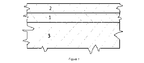
¨ Figure 1 illustrates the layer structure of a two-layer antireflection
coating according to the
present invention formed on a non-transparent substrate;
¨ Figure 2 illustrates the layer structure of a two-layer antireflection
coating according to the
present invention formed on a transparent substrate;
¨ Figure 3 shows wavelength dependence of the refractive index of the
transparent substrate
made of glass;
¨ Figure 4 shows wavelength dependence of the refractive index of the lower
(first) layer of a
two-layer antireflection coating according to the invention formed on the
glass substrate;
¨ Figure 5 shows wavelength dependence of the refractive index of the upper
(second) layer
of a two-layer antireflection coating according to the invention formed on the
glass substrate;
¨ Figure 6 shows transmittances measured at various angles of incidence for
the glass sub-
strate with and without (curves with "a") the antireflection coating;
¨ Figure 7 shows wavelength dependence of the refractive index of a
polycarbonate sub-
strate;
¨ Figure 8 shows wavelength dependence of the refractive index of the lower
(first) layer of a
two-layer antireflection coating according to the invention formed on said
polycarbonate sub-
strate;
¨ Figure 9 shows wavelength dependence of the refractive index of the upper
(second) layer
of a two-layer antireflection coating according to the invention formed on
said polycarbonate
substrate;
CA 03028375 2018-12-05
WO 2017/216592
PCT/HU2017/050023
-4-
- Figure 10 shows transmittances measured at various angles of incidence
for the polycar-
bonate substrate with and without (curves with "a") the antireflection
coating; and finally
¨ Figure 11 is a scanning electron (SEM) micrograph of the layer structure
of the antireflec-
tion coating according to the present invention formed on a glass substrate.
In the drawings, identical layers are designated with the same reference
numerals.
Figure 1 illustrates a two-layer antireflection coating applied on a side
surface of a substrate
3 of arbitrary shape made of a substance with refractive index nsubstrate,
wherein said coating
consists of a transparent first layer 1 with thickness di and refractive index
ni, and a trans-
parent second layer 2 with thickness d2 and refractive index n2 over the first
layer. In accord-
ance with the present invention the thicknesses and the refractive indices of
the first and
second layers 1, 2 satisfy the following conditions:
¨ thickness di of said first layer 1 ranges from 10 to 70 nm and the
refractive index ni satis-
fies the relation 1.05<ni<1.35 within the wavelength range of 375 to 1000 nm;
¨ thickness d2 of said second layer 2 ranges from 30 to 100 nm and the
refractive index n2
satisfies the relation 1.25<ni<1.5 within the wavelength range of 375 to 1000
nm; and
¨ ni<n2.
Such a two-layer antireflection coating can be formed on the substrate 3
through e.g. the so-
called "sol-gel" technique known in literature, preferably by means of a dip
coating technolo-
gy and then by conditioning the obtained coating under suitable conditions;
basic details of
the procedure can be known from e.g. EP-2,939,987 Al, and Chapter 10 "Dip
Coating" by
C. Jeffrey Brinker included in the textbook of Chemical Solution Deposition of
Functional Ox-
ide Thin Films (editors: T. Schneller, R. Waser, M. Kosec, D. Payne;
publisher: Springer Vi-
enna; published in 2013; ISBN 978-3-211-99310-1).
Figure 2 illustrates a similar structure on a substrate 3 that is transparent
at least within the
wavelength range of visible light. Here, the first and second layers 1, 2 are
equally applied on
both side surfaces of the transparent substrate 3. Transparency of the
substrate 3 is im-
portant here as light can strike the substrate 3 from both sides and
reflection can be reduced
in both directions in this case. Actually, transmittance, that is, the ability
of the substrate to
transmit light improves here.
Figure 3 shows the refractive index nsubstrate of the transparent substrate 3
made of glass as a
function of the wavelength of the incident light. Here and from now, the term
"glass" refers to
a glass substance that is permeable to light traditionally at least in a range
of the electro-
magnetic spectrum corresponding to visible light and thus is transparent.
CA 03028375 2018-12-05
WO 2017/216592
PCT/HU2017/050023
- 5 -
In Figure 4, the refractive index of the first layer 1 of an antireflection
coating arranged on the
substrate 3 is illustrated in a similar plot, wherein said antireflection
coating corresponds to
the structure according to Figure 2 and has been applied on both side surfaces
of the sub-
strate 3. Moreover, in Figure 5, the refractive index of the second layer 2 of
the same struc-
ture can be seen. In case of the specimen studied and measured, the layer
thicknesses are
as follows: for the first layer 1, thickness di is equal to 25 5 nm, i.e.
di=25 5 nm, and for the
second layer 2, thickness d2 is equal to 65 3 nm, i.e. d2=65 3 nm. According
to further ex-
periments performed, the substrate 3 can be made of a quartz glass as well,
instead of ordi-
nary glasses.
Figure 6 shows the transmittance as measured for the structure of Figure 2 as
a function of
the wavelength of the incident light. Here, curves 11, 12 and 13 represent the
transmittance
of said structure measured at the angles of incidence 0 , 40 and 70 ,
respectively; the
curves also designated by an index "a", that is, curves 11a, 12a and 13a show
the transmit-
tance of the substrate without the antireflection coating. One can read from
said curves that
the maximum of the transmittance shifts towards the range of smaller
wavelength as the an-
gle of incidence increases. For substrates 3 made of glass/quartz glass, the
transmittance of
the layers prepared with the above discussed parameters is higher than 70%
everywhere
within the wavelength range of 375 to 1000 nm and the range of angles of
incidence of 0 to
70 . It can also be seen from Figure 6 that, as a consequence of the
application of an antire-
flection coating according to the present invention, the light transmission of
a substrate made
of glass improves in a broad range of angles of incidence, practically over
the whole range of
0 to 70 , compared to that of a substrate without an antireflection coating
according to the
invention.
In Figure 7, refractive index of a substrate 3 made of polycarbonate is
illustrated. Here, the
layer structure is identical to the one shown in Figure 2. Wavelength
dependencies of the re-
fractive indices of transparent first and second layers 1, 2 of the
antireflection coating applied
on both side surfaces of the substrate 3 are shown in Figures 8 and 9. In this
case, thickness
di of said first layer 1 is equal to 50 4 nm, i.e. di=50 4 nm, and thickness
d2 of said second
layer 2 equals 35 3 nm, i.e. d2=35 3 nm holds.
Figure 10 is similar to Figure 6 discussed above but for a layer structure
formed on the poly-
carbonate substrate 3. Curves 21, 22 and 23 represent respective
transmittances at angles
of incidence of 0 , 40 and 70 , respectively; the curves also designated by
an index "a", that
is, curves 21a, 22a and 23a show the transmittance of the polycarbonate
substrate without
CA 03028375 2018-12-05
WO 2017/216592
PCT/HU2017/050023
- 6 -
the antireflection coating. For the polycarbonate substrate, the transmittance
of the layers
prepared with the above discussed parameters is higher than 73% everywhere
within the
wavelength range of 400 to 1000 nm and the range of angles of incidence of 0
to 70 .
Figure 11 is a micrograph of the layer structure shown in Figure 1 taken by a
scanning elec-
tron microscope (type: Leo 1540 XD with JSM-26 analogue electronics,
traditional electron
optics and digital image recording; distributor: Zeiss) at a magnification of
300000x. One can
readily see from said micrograph that the antireflection coating according to
the invention ap-
plied on the substrate 3 is provided by a two-layer layer structure that
consists of the first
layer 1 and the second layer 2, wherein the two layers are of different
optical properties.
According to our studies, it might also occur that the first layer 1 is formed
by a combination
of several sublayers, wherein the total thickness of said combination of
sublayers corre-
sponds to the thickness di of the first layer 1, the refractive indices of
said sublayers of the
combination preferably increase as progressing away from the substrate 3, and
all the refrac-
tive indices of the sublayers are within the range of refractive indices set
for the refractive in-
dex ni of the first layer 1 in the above-referred first embodiment of the
antireflection coating
according to the invention.
Alternatively, according to our studies, it might also occur that said second
layer 2 is formed
by a combination of several sublayers, wherein the total thickness of said
combination of
sublayers corresponds to the thickness d2 of the second layer 2, the
refractive indices of said
sublayers of the combination preferably increase as progressing away from the
substrate 3,
and all the refractive indices of the sublayers are within the range of
refractive indices set for
the refractive index n2 of the second layer 2 in the above-referred first
embodiment of the an-
tireflection coating according to the invention.
The substrate 3, optionally, may form the envelope of a light emitting device
or a part thereof.
In such a case, the decrease in the amount of light being generated inside
said envelope re-
flected by the internal surface of the envelope leads to an increase in the
luminous efficiency.
In a possible further case, the substrate 3 may form an optical lens,
including all kinds of im-
aging and other non-imaging lenses as well. For a skilled artisan, advantages
of the usage of
an antireflection coating according to the present invention (such as e.g.
higher light trans-
mission rates, images with higher contrast, easier recordability due to the
greater amount of
light passed through, etc.) are evident.