Note: Descriptions are shown in the official language in which they were submitted.
CA 03028575 2018-12-19
WO 2017/220847 PCT/F12016/050450
1
LED screen or illumination means with a flexible film structure
Field of the invention
The present invention relates to LED display and illumination devices arranged
in
a flexible thin film arrangement.
Background of the invention
LED (Light Emitting Diode) based display technology has emerged lately in many
various applications. Usually LEDs are used in flat panel displays where the
light
emitting diodes are formed in an array in order to create pixels for a video
display.
LED displays are currently used especially in outdoor signs and information
boards, and also e.g. public transport vehicles as information signs. RGB LEDs
can be used to create the colours in the video image.
Organic LEDs (OLEDs) have also been used in monitors and TV screens, for in-
stance. OLED technology is based on emissive electroluminescent layer made of
organic compound which is capable to emit light in response to an incoming
elec-
tric current. The electrodes which are connected to the organic layer may be
transparent.
Publication WO 2011/046961 (BML Productions Inc.) discloses a hermetically
sealed OLED display which can be positioned below a surface of an ice layer.
The
display layer is placed directly below the ice, and the display layer is on
top of a
chilled concrete layer which in turn can be piped in order to cool this layer.
The
chilled layer is separated from warmer base layers by an insulating layer.
Several
pieces of displays can be configured together in a grid-like arrangement, i.e.
in a
matrix-form.
Publication WO 2015/092140 (Flexbright Oy) discloses an illumination structure
which is implemented by a flexible and rollable thin film. It comprises a
polymeric
layer whose other side comprises a pattern (electronic circuit) layer which is
elec-
trically conductive and flexible. The structure comprises a hole for the LED
flip-
chip, which in turn is connected to the pattern layer through contact areas.
On top
of the LEDs and the polymeric layer, there is a flexible shielding layer. The
thick-
ness of the polymeric layer is mentioned to be less than 100 micrometers. The
light source film is manufactured with a roll-to-roll method.
2
Publication US 2013/0074538 (Forsberg) discloses a panel LED display which can
be
located under the ice surface of an ice rink. The LEDs are placed in
enclosures of the
panel, and there is a cooling apparatus which circulates the coolant through
the enclo-
sures in order to remove the heat generated by the LEDs. The panel of Forsberg
is a stiff
and rigid panel, and an acrylic sheet made of polymethyl methacrylate (PMMA)
polymer
is a preferable material for such a panel.
The prior art has a problem that current screen solutions have been mostly
rigid planar
panels which can only be attached on walls or placed on a support on a
surface. This has
led to the situation where locations and application areas of these devices
are restricted.
The flexibility of the current solutions is not always that good or not even
possible at all.
Also scalability regarding the given resolution of the LEDs and the
transparency are is-
sues which have not been so well handled in the past. Furthermore, current
manufactur-
ing methods have not been very cost-effective. Heat conduction has been a
problem in
some solutions.
Summary of the invention
The present invention introduces a layered and flexible thin film based LED
screen or
illumination module structure. The emphasis is in the structural elements in
the modules
forming the apparatus, and in the manufacturing method of such an apparatus,
and not
in the fully operational LED screen with all the required controlling means.
The inventive idea comprises various embodiments of a screen or illumination
module
structure, and also the connection principles between modules, and a
corresponding
manufacturing method of such screen or illumination module structures and
thus, the final
screen or illumination apparatus as well. Furthermore, a computer program or
several
computer programs may be used in implementing the manufacturing method into
prac-
tice.
Furthermore, the inventive idea comprises various uses of the screen
structures and illu-
mination modules in context with different installing platforms and
application areas.
As a summary, the present invention discloses a screen or illumination
apparatus, which
comprises:
Date Recue/Date Received 2020-08-14
3
¨ at least one module where each module comprises a layer arrangement of at
least
one layer, where at least one layer is at least partly made of a polymer,
¨ the layer arrangement comprises a LED layer arrangement of at least one
LED layer
which comprises a plurality of LEDs, where each single LED layer comprises
electrically
conductive patterns, where the LEDs are electrically coupled with the
electrically conduc-
tive patterns, and in case at least one module comprises at least two layers:
¨ the layers are stacked on top of each other for each module in order to
form the
layer arrangement for the at least one module, and in case at least two
modules are
formed,
¨ connecting the at least two modules together in order to form the
apparatus.
In one embodiment of the invention, the layer arrangement as such is at least
partly flex-
ible.
In one embodiment of the invention, the layer arrangement as such is at least
partly trans-
parent.
In another embodiment, the invention relates to a screen apparatus, wherein
the screen
apparatus comprises:
¨ at least one module wherein each module comprises a layer arrangement
compris-
ing at least one layer;
¨ wherein the at least one layer is at least partly made of a polymer;
¨ wherein the layer arrangement is at least partly flexible and comprises a
LED layer
arrangement of at least one LED layer which comprises a plurality of LEDs,
¨ wherein each of the at least one LED layer further comprises electrically
conductive
patterns and the LEDs are electrically coupled with the electrically
conductive patterns;
¨ wherein when the at least one module comprises at least two layers, the
at least
two layers are stacked on top of each other for each module to form the layer
arrange-
ment for the at least one module;
¨ wherein when the at least one module is at least two modules, the at
least two
modules are connected together to form the apparatus; and
Date Recue/Date Received 2020-08-14
4
¨
wherein the screen apparatus further comprises a plurality of through-holes in
at
least one layer to enhance transparency for the apparatus, to provide spaces
for LEDs of
an adjacent layer, to provide possibilities for at least one of air and water
to penetrate
through the screen apparatus, or any combination thereof.
In one embodiment of the invention, in the apparatus, when the apparatus is
set in a
planar form, a first part of the LEDs are directed to a first viewing
direction and a second
part of the LEDs are directed to a second viewing direction opposite to the
first direction,
resulting in a dual-sided display or illumination device.
In one embodiment of the invention, the apparatus further comprises a
plurality of holes
in at least one layer in order to enhance transparency for the apparatus,
and/or for provid-
ing spaces for LEDs of an adjacent layer.
In one embodiment of the invention, the functionality of a single layer is
selected from a
group of: a LED layer, a solar panel layer, an electrically conductive pattern
layer, a bat-
tery layer, a holed film layer, a physical support layer, a protective layer,
a thermally con-
ductive layer, a thermally insulating layer, a diffuser layer, a reflective
layer, an electrolu-
minescent emission layer, or a sensor layer comprising at least one dedicated
sensor.
In one embodiment of the invention, the apparatus further comprises a
plurality of mod-
ules placed adjacently side by side with a butt joint, or fixed together by
the connecting
means.
In one embodiment of the invention, the protective layer or means further
comprises pro-
tective polymer strips of film placed adjacently to one another, or a layer of
film, on at
least a part of the surface area of the apparatus, or a single protective
strip provided on
top of the seam between two adjacent modules of the apparatus, or a sprayed
material
on at least a part of the surface area of the apparatus, or a polymer material
which has
been injection molded on at least a part of the surface area of the apparatus.
In one embodiment of the invention, the apparatus further comprises a frame
structure
where the at least one module is fixed to, and wherein the frame structure
comprises
electrically conductive wires which are connectable to the selected locations
of the mod-
ules through connecting means.
Date Recue/Date Received 2020-08-14
5
In one embodiment of the invention, selected layers of a single module, and/or
selected
layers of adjacent modules are fixed and/or electrically coupled by connecting
means,
where the connecting means is made of an electrically conductive material.
In one embodiment of the invention, the electrically conductive pattern of the
selected
layer is electrically coupled to the connecting means by a connection securing
means
when the connecting means is in place, and where the connecting means is
conductive,
and where the connection securing means is an additional section of
electrically conduc-
tive wire pressing onto the connecting means, and/or conductive adhesive
placed around
the connecting means.
In one embodiment of the invention, the apparatus comprises:
¨ one or two LED layer arrangements,
¨ one or two solar panel layers, and
¨ at least one battery layer,
¨ arranged in an order, where the solar panel layer or layers are able to
collect light
energy either directly as an outermost layer or through the at least partly
transparent
layers of the screen or illumination apparatus, resulting into a one- or dual-
sided screen
or illumination apparatus.
In one embodiment of the invention, the LED layer arrangement is combined with
another
LED layer arrangement, where the latter LED layer arrangement has been flipped
180
degrees before the combining, in order to achieve a dual-sided LED screen or
illumination
apparatus.
In one embodiment of the invention, the apparatus further comprises wireless
connectiv-
ity means.
In one embodiment of the invention, the apparatus further comprises loT
connectivity
means.
According to the second inventive aspect of the invention, a manufacturing
method for a
screen or illumination apparatus is disclosed. The manufacturing method
comprises the
steps of:
Date Recue/Date Received 2020-08-14
6
¨ manufacturing at least one LED layer, each LED layer comprising a
plurality of
LEDs, where at least one LED layer is at least partly made of a polymer,
¨ where each single LED layer comprises electrically conductive patterns,
where the
LEDs are electrically coupled with the electrically conductive patterns,
¨ creating a layer arrangement for a single module by stacking the at least
one LED
layer and possible other layers in a desired order, and repeating the creating
step in case
of a plurality of modules are desired; and in case at least two modules are
formed,
¨ connecting the at least two modules together in order to form the
apparatus.
In another embodiment, the invention relates to a manufacturing method for a
screen
apparatus, wherein the manufacturing method comprises the steps of:
¨ manufacturing at least one LED layer, each LED layer comprising a
plurality of
LEDs, the at least one LED layer being at least partly made of a polymer and
comprising
electrically conductive patterns, where the LEDs are electrically coupled with
the
electrically conductive patterns;
¨ creating a layer arrangement for a single module by stacking the at least
one LED
layer and eventually at least one further additional layer in a desired order,
and repeating
the creating step when at least two modules are formed, the layer arrangement
being at
least partly flexible;
¨ wherein when at least two modules are formed, connecting the at least two
modules
together form the apparatus; and
¨ providing a plurality of holes across the screen apparatus to enhance
transparency
for the apparatus, to provide spaces for LEDs of an adjacent layer, to provide
possibilities
for at least one of the air and water to penetrate the screen apparatus, or
any combination
thereof.
In one embodiment of the manufacturing method, printing the electrically
conductive pat-
terns and component assembling steps are performed with a roll-to-roll method.
In one embodiment of the manufacturing method, stacking the layers on top of
one an-
other, where each LED of a LED layer will be accommodated in a corresponding
hole of
a next layer, or vice versa.
Date Recue/Date Received 2020-08-14
6a
In one embodiment of the manufacturing method, placing or spraying or
injection molding
a protective layer on at least a part of the surface area of the apparatus.
In one embodiment of the manufacturing method, stacking a first layer
arrangement in
order to achieve a first single-view apparatus with at least one LED layer,
stacking a
second layer arrangement in order to achieve a second single-view apparatus
with at
least one LED layer, flipping the second layer arrangement 180 degrees, and
attaching
the first layer arrangement with the flipped second layer arrangement in order
to achieve
a dual-view apparatus.
In one embodiment of the manufacturing method, stacking four LED layers, with
each
LED layer having a first distance between LEDs in both X- and Y-directions on
the surface
of the LED layer, on top of one another so that a first and a second LED layer
have a
misplacement in an X-direction, and a third and a fourth LED layer have a
misplacement
in an X-direction, and stacking these two pairs of LED layers with a
misplacement in a Y-
direction, resulting in a LED layer structure which has half of the first
distance between
LEDs in both X- and Y-directions on the surface of the LED layer structure.
In one embodiment of the manufacturing method, stacking a plurality of LED
layers,
where LEDs (52) on each of the LED layers (51a-e) have an identical
distribution, and
when stacking the LED layers in a misplaced manner, achieving a LED layer
structure
where the LEDs have a uniform distribution in X- and Y-directions on the
surface of the
LED layer structure.
In another embodiment the invention relates to the manufacturing method
defined here-
inabove, characterized in that the manufacturing method further comprises:
stacking a
number X of LED layers on top of one another so that adjacent LED layers have
a
misplacement d in a first direction, with LEDs in each LED layer having a
distance X times
d between LEDs in the first direction on the surface of the LED layer,
resulting in a LED
layer structure where the LEDs have a distance d in the first direction on the
surface of
the LED layer structure.
In one embodiment of the manufacturing method, the possible other layers are
taken from
the group of: a solar panel layer, an electrically conductive pattern layer, a
battery layer,
a holed film layer, a physical support layer, a protective layer, a thermally
conductive
Date Recue/Date Received 2020-08-14
6b
layer, a thermally insulating layer, a diffuser layer, a reflective layer, an
electrolumines-
cent emission layer, or a sensor layer comprising at least one dedicated
sensor.
Brief description of the drawings
Figure 1 illustrates a modular structure of a LED thin film screen,
Figure 2 illustrates a construction principle for modules of the LED screen,
Figure 3 illustrates a structure comprising protective strips of film,
Figure 4a illustrates a creation of a four-layered structure of the films
comprising LEDs,
Figure 4b illustrates a cross-sectional view of two adjacent columns of LEDs
with holes
in the four-layered structure of Figure 4a,
Figure 4c illustrates an example of three stacked layers, where each single
layer accom-
modates single-colored LEDs, for forming a single RGB pixel,
Figure 5a illustrates a 5-layer structure in order to create a LED screen with
a dense
resolution, as a side-view,
Figure 5b illustrates the multi-layered LED screen of Figure 5a as a top-view,
with LED
spots visible,
Figure 6a illustrates a pinhole for the pin in a single layer with a
conducting wire,
Figure 6b illustrates a connection principle for a 4-layered structure,
Figure 6c illustrates a cross-section of the pin-connected screen modules with
inter-layer
conductivity between two different layers of two adjacent screen modules,
Date Recue/Date Received 2020-08-14
CA 03028575 2018-12-19
WO 2017/220847 PCT/F12016/050450
7
Figure 6d illustrates an example for connecting a single module with a 4-layer
structure to the frame with a plurality of pins,
Figure 6e illustrates an example for connecting two adjacent modules with 4-
layer
structures to the frame with a plurality of pins,
Figure 6f illustrates examples of connecting two modules with a pin, a
counterpart
and adhesive glue,
Figure 7 illustrates an embodiment of a printed pattern on the layered
structure
with pin locations shown along the electrically conductive patterns,
Figure 8a illustrates a three-layer example of the screen structure,
Figure 8b illustrates a six-layer example of the screen structure,
Figure 8c illustrates another three-layer example of the screen structure,
Figure 8d illustrates an embodiment of a dual-sided screen and illumination
struc-
ture with holes and viewing directions in two opposite directions from the
thin-
filmed screen structure, and
Figure 8e illustrates an embodiment of a dual-sided screen and illumination
struc-
ture, with two 4-layered structures placed with their backs facing each other.
Detailed description of the embodiments
The present invention introduces layered and flexible thin film_based LED
screen
and illumination device structures to display full-color or black-and-white
still imag-
es or video for visually displaying information, or for illuminating purposes.
The de-
vice comprises at least one module where each module comprises at least one
layer where different layers may have different functionalities. In the
following,
where merely the screen structure is discussed, it is meant to include both
the dis-
playing devices and illumination devices. The screen structure may comprise a
LED layer comprising a plurality of LEDs and desired electrical circuitry
meaning
electrically conductive patterns with contact areas for components. In case
the
structure comprises several LED layers, the corresponding structure is
referred as
a LED layer arrangement. In a similar fashion. In some embodiments of the
inven-
tion, the structure may comprise electric energy collecting means such as e.g.
a
solar panel, and electric energy storage means such as at least one
accumulator
unit or battery. All these functions may be implemented with a single main
func-
CA 03028575 2018-12-19
WO 2017/220847 PCT/F12016/050450
8
tionality per a corresponding layer, e.g. a battery can be formed through
having
one or more battery layers among the layered structure. In case the structure
comprises several battery layers, the corresponding structure is referred as a
bat-
tery layer arrangement. The battery or batteries can preferably be
rechargeable,
which can be used for storing solar energy, for instance. Alternatively,
instead of a
battery layer (arrangement), an external battery means may be used. A single
electrically conductive layer may be patterned for creating conductors of an
elec-
tric circuit which enable the operation of the screen or illumination device.
In an
example, electrical circuitry comprises the input supply of the electric
current for
.. the LEDs, and also a control signal which is used to drive the LEDs in
order to
create the desired image. Because LED types are various, it is meant that
appro-
priate wirings of electrical conductors are selected for the selected LEDs. Of
course, different layers require dedicated electrical circuitry as well. In
the inven-
tion, the electric supply can be provided from mains current to the LED
screen. In
another embodiment, the screen structure has an independent electric supply
cre-
ation means, e.g. through a solar panel layer along the structure. A part or
all
these functional parts can be implemented as a layered element or by
connecting
or adding elements or material onto a layer where a single layer can be
manufac-
tured as thin, transparent and flexible, and the surface dimensions of a
single layer
are freely scalable and selectable according to the used application.
In the present invention, the used LEDs in the structure are non-organic LED
components. Furthermore, the used LEDs may be encapsulated one or multi-color
SMD LED components, or alternatively bare LED chips may be used.
The screen structure comprises at least one layer manufactured from a polymer
like plastic, or from several different polymers. In the following where
plastic has
been disclosed as an example, a polymer material is generally meant to be used
as a base material for a single layer. Plastic layers can be formed e.g. from
polyi-
mide, PET, PEN, polycarbonate or liquid crystal polymer. The electric
circuitry can
be formed through circuit patterns on top and/or on bottom of the plastic
layer by
using etching, transfer printing methods, a combination of evaporation and
electro-
lytic deposition, patterning through mechanical machine tooling or laser
ablation,
or by printing with at least one printable conductive ink. In addition to
traditional
conductive materials such as copper or silver, other conductive materials such
as
ITO (indium tin oxide) or GraphExeter can be used in electrically conductive
pat-
terns. The polymer materials itself have many advantages, because it is light-
weighted, it can be manufactured as a thin element, and it is capable to bend
and
CA 03028575 2018-12-19
WO 2017/220847 PCT/F12016/050450
9
even twist into different shapes, and placed onto or into a specially shaped
physi-
cal structure without breaking. Furthermore, many plastic materials are also
trans-
parent in view of visible light so that light emitted by the LEDs can
propagate
through the plastic layer without too much attenuation. As a result, the whole
struc-
ture can be made transparent to a certain extent which is helpful in many of
the
embodiments.
In one embodiment, a plastic layer can be provided with small through-holes,
where the hole diameter and density (number of holes) per surface area can be
freely selected. The use of holes will enhance the transparency regarding the
visi-
ble light, and it also provides possibilities for the air and water to
penetrate through
the plastic layer if it is a desired feature of the screen structure. Also as
a benefi-
cial embodiment, the size and shape of a hole within a plastic layer is
selected to
fit with a LED of an adjacently locating layer. This means that the LED of a
next
layer will be fitted into the hole of the layer, resulting in a smooth and
bunnpyless
planar structure. In this embodiment, the number and density of holes within a
sur-
face is thus at least the number and density of LEDs within a single layer.
When
the layers are stacked on top one another, there can be a hole in all other
layers
within the location of the LED in a single layer, resulting in a good
visibility of the
LED through the layered structure even if the number of layers is larger.
In case a simple one-layer structure is used as a platform for the LEDs, it
does not
necessarily need to include any holes because the lack of any adjacent layers.
Still, if holes are used in the one-layer structure, it would enhance e.g.
transparen-
cy.
In one embodiment of the invention, it is referred to a modularly formed LED
screen structure shown in Figure 1. The illustration exemplifies a LED screen
10
where the LED screen comprises a plurality of screen modules which are fixed
on
a frame structure 12. The frame structure 12 is preferably a rigid element and
it
can be shaped in a planar or non-planar shape. In one example, it is possible
to
install power supply and signal cablings inside or along (placed on top of)
the
frame structure 12, where they are also better protected from physical
twisting
movements or harmful moisture, for instance. A single module 11 of the whole
structure may be a longitudinal strip, or it may be a piece-like module with
desired
dimensions. In Figure 1, the frame structure 12 comprises horizontal bars
within a
rectangular frame. The modules 11 are shown as vertical strips and they are
placed adjacently with each other so that all strip-shaped modules are placed
or-
CA 03028575 2018-12-19
WO 2017/220847 PCT/F12016/050450
thogonally in view to the horizontal bars of the frame 12. In that case, the
modules
11 can be fixed to the frame 12 in locations, where these two elements
intersect.
The frame structure 12 can comprise electrically conductive wires, which can
be
connected to desired locations of the modules. Alternatively, some sections or
the
5 whole frame structure can be built without wires, and especially, if only
a single
module is used in the apparatus.
In another embodiment, it is possible to place modules 11 in parallel
direction with
the horizontal bars of the frame 12 (not shown in Figure 1). In that case, the
edges
of the each module 11 can be fixed to the frame 12 along the whole edge, or
just
10 in designated locations along the edge.
In one embodiment, the strip-shaped modules 11 or piece-like modules can be at-
tached to the frame 12 by using a plurality of connecting means. The
connecting
means may be made of either conductive or insulating material. The connecting
means may be e.g. pins, but various other elements can also be used for this
task.
For simplification, pins are discussed in later embodiments. In practice, the
two ad-
jacent modules can be both attached to the bar of the frame 12 with a linear
as-
sembly of pins. The pins can be electrically conductive, and they can be used
for
instance for feeding electric supply carried by the wirings in the frame
structure to
certain designated points in the screen structure. However, some of the pins
may
be insulating (i.e. non-conductive) material, and such pins may be used in
attach-
ing the modules to the frame structure. Thus, the pins may be either conductor
pins or insulator pins, and this applies to other used connecting means as
well.
Concerning alternative options for pins, other connecting means such as
screws,
studs, spikes, crimp connectors or also other connecting arrangements can be
used.
Concerning the example of Figure 1, the pin connection points can be selected
e.g. in the "corner points" where the edges of a module coincide with the
frame
sections. Additional connection points between the pins and the frame
structure
can be selected along the seams between two adjacent modules, or along the
frame sections, e.g. with uniform spacings.
In another embodiment, the pins can be arranged to fix several layers together
e.g. in a line-shaped arrangement. It is possible to place the pins through
e.g. one
or two overlapping layers and fix these layers onto the frame. This is
especially
CA 03028575 2018-12-19
WO 2017/220847 PCT/F12016/050450
11
beneficial with the layer structure where layers are a little bit misplaced
between
each other, in order to place the LEDs uniformly to the whole structure. These
as-
pects are disclosed in more detail in connection with Figures 4 and 5a.
One option for supplying additional electric current to the screen structure
can be
created by placing additional electrically conductive patterns on one or both
sur-
faces of a given plastic layer. Such a plastic layer may be specifically used
just for
the electrically conductive patterns. Another option is to add these
electrically con-
ductive patterns to other functional layers which already e.g. comprise LEDs
and
the related circuitry regarding the controlling of the LED screen output.
Generally,
the conductive patterns for the LED power supply can be implemented in any of
the layers because different layers can be electrically connected between mod-
ules, see the later disclosure. Electrical power supply wirings integrated in
the
frame structure will help in providing the electrical power supply in a
uniform fash-
ion across a larger screen structure. Also wirings for other desired purposes
may
be added in the frame structure. These other purposes may be used for a
control
signal or for carrying some measurement signals achieved through dedicated sen-
sors.
In the following, the screen structure is discussed without incorporating any
rigid
frame as a support structure for the layered screen. Instead, the focus is in
the
layered structure of the film-based screen, and also in the protective means
used
to protect the layers from external substances and also for fastening the
strips bet-
ter together. This kind of a simplified structure is illustrated in Figure 2.
A single
functional layer of the whole screen can be comprised of several strips 20 or
bands of thin film. Such a plurality of parallel and longitudinal strips 20 in
a single
plane can be placed together with butt joints which are formed along the side
edg-
es of the strips, i.e. the strips 20 can be placed on a single plane in a
parallel ar-
rangement without any gaps between the edges of the strips or any overlapping
sections between two adjacent strips of film. Figure 2 shows the installment
of the
strips 20 by placing longitudinal strips besides each other so that long edges
of the
strips will be placed adjacently with a butt joint. The length of the strips
20 can be
selected according to the desired application, i.e. according to the required
screen
dimension; in other words, the strips can be cut in a desired length. In one
embod-
iment, the seam formed as a butt joint can be secured together by a tape or
other
adhesive band placed on top of the butt joint. In practice, such a tape is
added be-
neath the layered structure to cover the seam.
CA 03028575 2018-12-19
WO 2017/220847 PCT/F12016/050450
12
In case only a single functional layer is constructed through a plurality of
narrow
film strips for the LED screen structure, there needs to be some appropriate
bond-
ing means within the structure which connects the film strips together. This
can be
implemented by placing protective strips of film in an orthogonal direction on
top of
the butt joint strips. Alternatively, the protective film strips can be placed
below the
functional layer of the LED screen. Of course, in an embodiment, the
protective
strips may be placed on both surfaces of a single strip which makes the
structure
even more protected. It is beneficial that the protective strips of film are
transpar-
ent. Protective strips may be added to the structure either to a single
module, or to
the whole screen or illumination device.
The layer shown in Figure 2 need not to be formed from longitudinal strips but
in-
stead, it may well be manufactured as a single planar film-like element in
desired
size and dimensions.
The simplified embodiment with a single-sided protection and connection is
illus-
trated in Figure 3. After the desired number of strips 20 have been put in
place e.g.
on top of a working face used in assisting the manufacturing work itself,
protective
strips of film 30 can be rolled over the strips 20 in an orthogonal direction
as it is
shown in Figure 3. Another possibility is to place the protective strips of
film 30 in a
same direction on top of the strips 20, but misplaced so that the butt joints
of the
strips 20 will locate below e.g. the inner part of the protective strip 30
(i.e. not ex-
actly below the seam). The protective strips 30 can be placed in an adjacent
man-
ner, one by one, next to the previously set protective strip. The resulting
structure
is a more robust one and also more secure laminated structure which keeps the
possible moisture and dirt better off the functional LED layer regardless of
the ap-
plication area or the location of the LED screen.
Regarding the material of the protective strips or a protective layer or tape,
it can
be made of plastic, epoxy, silicon or generally from one or more synthetic
polymer-
ic material.
Such a protective layer may be created through spraying liquid material such
as
insulating protective lacquer. Another kind of protective layer may be manufac-
tured through spraying or injection molding e.g. plastic on top of the screen
struc-
ture, resulting in a plastic covered screen structure. Such a plastic layer
may be
shaped appropriately with the screen structure, in order to create e.g. a
desired 3-
D shaped form for a base object, provided with a screen structure on an outer
sur-
face of the base object, and a protective layer on top of the screen
structure. Gen-
CA 03028575 2018-12-19
WO 2017/220847 PCT/F12016/050450
13
erally, the protective layer is at least partly transparent and it protects
the laminat-
ed screen from e.g. dust and moisture. Regarding the shapability of the
laminated
screen into different shapes, it will naturally diminish as a function of the
increasing
thickness of the laminated structure. By selecting an appropriate plastic type
and a
suitably small thickness of a single layer, this aspect can be improved for
multi-
layer structures.
In another embodiment, there can be a small gap between two adjacent strips of
active layers 20, instead of a butt joint. Because the protective strips 30
will fix the
layered structure together after their installment, such a gap is not harming
the ro-
bustness of the layered structure. Instead, it makes sure that no overlapping
edg-
es will locate on top of another layer when the layered structure is
manufactured.
Regarding the protective strips of film 30, they can be installed with butt
joints be-
tween the long edges of one another. In an alternative embodiment, the
protective
strips 30 can be placed in a slightly overlapping fashion when considering the
ad-
jacently locating strips. If such a structure is placed in an inclined
position, the
overlapping structure of the protective films ensures that e.g. water flowing
on top
of the screen structure will flow along and out of the surface of the
structure with-
out entering into the structure, i.e. between the layers. The protective
strips 30
thus resemble roof tiles of a ridge roof in its principle regarding the
flowing water
on top of it.
The stacked layers according to the invention can be provided with a
protective
layer on top of all the layers, either one-sidedly or dual-sidedly in case of
a dual-
sided screen. In case holes are used in the layers, each LED will be topped
only
by the protective layer, making the transparency of the structure uniformly
good,
because different LEDs will be attenuated only by the attenuation of the
protective
layer.
In another embodiment of the whole screen structure, the structure can be manu-
factured through applying several LED film layers stacked on top of each
other.
The result is a multi-layered, or in other words, a laminated structure. In
one ex-
ample, each film layer can be a piece of plastic layer with appropriate number
of
LEDs attached to it with selected distances between the LEDs. Different layers
may be identical or there might be some differences e.g. regarding the LED
densi-
ty along the layer surface. The structure may also comprise intermediate
layers
which do not incorporate any LEDs. The layers may comprise holes so that the
LEDs of an adjacent layer can be positioned in the holes of the subsequent
layer,
CA 03028575 2018-12-19
WO 2017/220847 PCT/F12016/050450
14
in order to enable a uniformly thick layered structure. The details of the
structural
options are discussed later.
The stacked group of layers may comprise a diffuser layer. The protective
layer on
top of the stacked layer group may act as a diffuser as well. Still, the
diffuser layer
may be a separate layer among the stacked group of layers. The diffuser layer
smooths the emitted light in order to enhance the visual experience of the
screen
or illumination means.
The stacked group of layers may comprise a reflective layer which reflects the
light
emitted in a LED to a desired direction. Furthermore, an electroluminescent
emis-
sion layer may be used.
In one embodiment, in addition to traditional manufacturing methods for
electrically
conductive patterns and assembling of components, the conductive patterns can
be formed by printing with at least one conductive ink, and the assembling of
com-
ponents can be performed by using a roll-to-roll method. This comprises
automat-
ed methods where electrically conductive patterns can be formed and the LED
components can be assembled to the layer structure, and the structure can be
moved into and from the manufacturing area in a controlled manner.
Furthermore, the manufacturing of the combined layer arrangement can be per-
formed one module at a time or by using a roll-to-roll based method. With such
a
method, the layered structure can be created by adding one layer at a time
onto
the previously created layer stack. The next layer can be released from a roll
and
directed to the manufacturing area where the combining of the layers takes
place.
It is also possible that all layers are initially stored in a rolled or planar
form and
starting from such an initial position, they are simultaneously released into
the
manufacturing area. When the layered structure is finished and e.g. treated by
heating, if desired, the complete layered structure can be set in a roll-
shaped form
again. This enables easy storage and transport for the complete layered screen
structure.
Figure 4a illustrates a stacking principle for a plurality of layers in order
to manu-
facture a screen structure, where each layer comprises a group of LEDs in this
example. In this embodiment of the manufacturing method, a so-called two-plus-
two layer structure is discussed. At first, two mutually similar film layers
41a, 41b
are taken into use. The upper layer 41a of the pair comprises LEDs 43a (marked
with unbroken circles), and their mutual distances in both the X- and Y-
directions
15
are the same, i.e. the LEDs are uniformly distributed across the plastic layer
surface. The
lower layer 41b is marked with dash lines. LED components are shown as
elements 43b
(marked as dashed circles) in the lower layer 41b. When these two layers 41a,
41b are
stacked in a superposed manner, the layers 41a, 41b can be placed so that the
LEDs 43a-
b of two consecutive layers will not coincide on top of one another but the
layers overlap in
a misplaced manner. The misplacement length between the two layers is selected
as half
the distance of the two adjacent LEDs 43a. This is illustrated in the top
illustration of Figure
4a, where there are two overlapping LED layers 41a, 41b stacked on top of each
other so
that the locations of the LEDs 43a of the first layer 41a will alternate with
the locations of
the LEDs 43b of the second layer 41 b, when looking at the structure from a
top view. The
resulting intermediate laminated film structure will have a double density of
the LEDs, when
looked at on top of the dual-layer structure. The middle illustration of
Figure 4a shows a
further dual-layer structure, which has practically the same structure as
above. The second
dual-layer structure is formed from the third layer 41c provided with LEDs
43c, and the
fourth layer 41d provided with LEDs 43d. The third and fourth layers are
misplaced similarly
as in the top illustration (i.e. moving the other layer in the X-direction).
Finally, these two dual-layer structures are stacked together so that there is
a
misplacement in the Y-direction between the dual-layer intermediate
structures. As a result,
a denser structure of LEDs is achieved in the final four-layer structure 42
shown in the
lowermost illustration of Figure 4a. The uniform line illustrates the top
layer with LEDs and
the dash lines show the other three layers with LEDs beneath it.
This results in a uniform structure and density among the LEDs which is highly
desired in
screen and illumination applications. Preferably, all of the layers are
selected to be
transparent except the lowermost layer may be either transparent or a non-
transparent
layer, in order to let the light emitted by the LEDs to propagate well through
the layered
structure. Because the films are highly transparent (preferably made of a
polymer, or
several polymers), the LEDs 43b-d in the lower layers 41b-d will have the same
visibility in
practice as the LEDs 43a of the top layer 41a have.
In an embodiment, the layers are provided with holes, such that the LED of a
lower layer
will be set below hole locations of the upper layers, resulting in higher
visibil-
CA 3028575 2019-03-22
CA 03028575 2018-12-19
WO 2017/220847 PCT/F12016/050450
16
ity of the LED from the top of the structure. In this regard, Figures 8d-e
explain
these optional solutions in more detail.
In a single layer like layer 41a, the gaps between the adjacent LEDs 43a can
be
provided with holes regarding both the X- and Y-directions. These holes will
then
locate exactly on the LED spots of the other layers when the stacking has been
completed for the layers. This enhances the transparency even more, and it
also
enables a smooth stacking for the layers even in the case, where the physical
thickness of a LED component is relatively large. The hole size and shape can
then be approximately the same as the LED size and shape in its outer edges,
thus making a good fit for the LED into the space defined by the hole.
Figure 4b illustrates two adjacent columns of LEDs according to the stacking
prin-
ciple shown in Figure 4a. At first the upper image is discussed. For a first
selected
column of LEDs, the first two layers 41a and 41b are transparent polymer
layers
without LEDs in this column. Holes are provided in these layers in places
where
the LEDs may locate in the other layers. The layers with LEDs present in this
col-
umn are layers 41c and 41d. The lower image of Figure 4b shows an adjacent
column to the first selected column of LEDs. In there, the layers with LEDs
present
in this column are the two uppermost layers 41a, 41b. The transparent polymer
of
the two other layers 41c and 41d are shown below the layers with the LEDs.
Such
cross-sections will alternate when different columns of LEDs are looked at. As
a
result, the LEDs locate at slightly different "heights" of the layered
structure but
when the structure is looked from greater distance on top of the planar
structure,
but such a difference can not be noticed during actual viewing.
In one embodiment, it is further possible to increase the LED density (and
thus,
the resolution of the LED screen) by the factor of four by repeating the
process ac-
cording to Figure 4a. In this manner, e.g. a 16-layer screen structure can be
manu-
factured with uniform distances between any two adjacent LEDs.
Both the 2-layer structure and the 4-layer structure have edge sections on
their
sides which can be used in connecting the screen sections or strips together.
This
can be performed by having an adhesive material in the inner surfaces of the
edge
sections. With inner surfaces, it is meant other surfaces than the top surface
of the
topmost layer or the bottom surface of the lowermost layer. With such an ar-
rangement, it is not necessarily needed to use pins in connecting the group of
lay-
ers modularly to one another. With glue or other adhesive used in the seams,
the
adjustability and flexibility of the screen structure is maintained. Of
course, the
17
connection of modules or strips with adhesive can be combined with the
connection with
e.g. pins into a metal frame, as shown in Figure 1. This means that a single
screen film
strip of a module 11 of Figure 1 can then comprise a multi-layer strip stack,
such as the
LED layer structure 42 of Figure 4a (lowermost illustration).
Regarding the connection in the seams of the layers, an alternative solution
to the use of
adhesive material is to use an adhesive tape on top of the seam of the
completely stacked
layer structure. The adhesive tape may be a protective plastic strip or layer
which is
connected with adhesive material to the lowermost or topmost layer.
Generally speaking, the protective layer or means or even the tape on the seam
area can
act as connecting means between the modules.
In an embodiment of the invention, each used LED is an encapsulated ROB LED or
an
encapsulated RGBW-LED. Alternatively, the used encapsulated LEDs may be merely
single-color LEDs, such as R- (red), G- (green), B- (blue) or W-LEDs (white).
Alternatively,
bare LED chips may be used instead of the encapsulated single-color LED chips.
The
required wiring and control method of the LEDs is selected based on the
selected type of
the LEDs.
In one embodiment of the invention, a layer structure may comprise four LED
layers,
among which a layer of R-LEDs acts as a first layer, a layer of G-LEDs acts as
a second
layer, a layer of B-LEDs acts as a third layer and a layer of W-LEDs acts as a
fourth layer.
In a further example comprising three separate layers where a single layer
accommodates
single-colored LEDs, Figure 4c is referred to. The first layer is provided
with R-LEDs, the
second layer is provided with G-LEDs and the third layer is provided with B-
LEDs. Of
course, the order of these layers for single-colored LEDs may be different
than the above
mentioned order. All these layers are provided with the same electrically
conductive pattern
capable of connecting between one another electrically. Thus, the vertical and
horizontal
wires of the matrix-type of pattern will coincide when the three layers are
stacked on top of
one another. As a result, a RGB screen or illumination device can be created
by the layered
structure by using different groups of single-colored LEDs.
According to yet another option of the invention, the LEDs of the first layer
may be aligned
180 degrees to the other direction than the LEDs of the second layer, after
the stacking. In
other words, the pointing directions between these two groups of LEDs are then
completely
opposite to one another. Different possibilities for create-
CA 3028575 2019-03-22
CA 03028575 2018-12-19
WO 2017/220847 PCT/F12016/050450
18
ing the dual-sided screen or illumination structure are discussed in
connection with
Figure 8d and 8e. This results in a thin film based LED screen structure which
is
double-sided and capable to show image information and/or illumination to two
to-
tally opposite directions. Such a structure has many interesting application
areas,
such as using them in two-sided advertisement signs, traffic signs or traffic
lights.
Further options comprise general information or guiding screens in public
spaces,
in advertising arrangements, or in various transport hubs such as train
stations.
The screen structure of the present invention may be used in architectonic
media
surfaces, such as placed within or on top of a window glass of any building or
on
other transparent "wall", or such as within a transparent overhead shade
structure
of an entrance door of a building, for instance. Other imaginable application
areas
comprise entertainment, cultural and artistical applications where
illumination
based effects and visual presentation is applied. These can be various,
ranging
from gaming applications (such as in escape games or in laser tag gaming
areas)
into cultural or educational venues (show arenas, theatres, sports venues,
audito-
riums, classrooms, lecture halls), and further into decorative or guiding uses
in ur-
ban landscape (name signs within a store entrance) or even in designed attrac-
tions of an amusement or theme park.
Of course these different application areas may use a single sided screen or a
double sided screen, depending on the application and also depending from the
type of an object or surface where the screen structure is embedded.
Because the layer structure is flexible, the dual-sided screen structure is
not mere-
ly restricted to planarly formed screens but also curved or otherwise shaped
ones
can be created as dual-sided screens. In one embodiment, the screen structure
can be a segment of a cylindrical shaped form, e.g. a planar TV screen which
has
been reformulated in an arc-shaped form.
In cases where the screen structure is implemented for e.g. educational or
busi-
ness related use such as in a classroom or in a meeting room, the screen struc-
ture can be connected through wireless communication means to a portable or
fixed device which can be accessed by a presenter in the room. Such a device
can
be a smartphone, a tablet or a laptop computer of a presenter or teacher who
can
then control the display screen information with such a portable device. Of
course
the controlling device can also be fixed in the meeting room or the classroom.
These arrangements will replace the traditional writing boards and
chalks/marker
CA 03028575 2018-12-19
WO 2017/220847 PCT/F12016/050450
19
pens in the classrooms and correspondingly, the projectors and cinema screens
used traditionally in various meeting rooms.
Generally, the screen structure according to the invention can be an loT
("Internet
of Things") device.
In a further example shown in Figures 5a and 5b, there are five LED layers
51a¨e
stacked on top of one another. A single layer acts as a single structural
element
for the screen structure which is constructed in the way discussed in the
following
embodiment. In this example, the five identical layers are each slightly
misplaced
compared to the previous layer so that the misplacement length is 1/5 of the
dis-
tance between two adjacent LEDs of a single layer. The resulting stacked
laminate
structure 51a¨e is shown as a top view in Figure 5b, with the LED elements 52
vis-
ible. The resulting LED density is five times thicker than the LED density in
a sin-
gle layer. In one embodiment, such a laminated structure may further be
covered
from one or both end surfaces by protective strips or a protective layer.
In one embodiment, the LEDs 52 on a single layer 51a may be aligned in direct
and parallel lines and the lines of LEDs may have a selected distance between
them. By misplacing the other layers in a fashion disclosed in the previous
para-
graph, the resulting structure will have the lines of LEDs combined into a
group of
LEDs where all LEDs are uniformly distributed in both X- and Y-directions of
the
layer structure. When the laminated or stacked layer structure is looked at
from an
orthogonal direction to the surface of the layer structure, the LEDs locating
on the
lower layers will also be visible because the layers are at least partly
transparent.
The mutual distances of the LEDs are the same in both X- and Y-directions. In
the
example of Figure 5b, one fifth of all the LEDs 52 locate as LED lines on
layer 51a,
.. and so forth.
By generalizing the idea of Figures 5a and 5b, the resolution of the screen
struc-
ture can be effectively selected by choosing an appropriate number of layers
with
an identical LED layout, and stacking them on top of one another with a slight
mu-
tual displacement between each and every two adjacent layers, as shown in Fig-
ure 5a. The transparency characteristics of the group of stacked layers will
define
the reasonable maximum number layers which can be stacked together. Further-
more, holes can be used in the layers, and it is also notable that the density
of
holes in the layers also affect the transparency of the layered structure.
CA 03028575 2018-12-19
WO 2017/220847 PCT/F12016/050450
In long structures (e.g. for long film strips as in Figure 2) there is a
possibility to in-
clude in the structure an intermediate layer which supplies additional
electric cur-
rent to the LEDs by placing electrically conductive patterns in appropriate
contact
points along the patterns of contact points of an adjacent layer. This enables
the
5 electric supply to be divided even more into a large screen structure,
where a cur-
rent of a single supply line remains within specified limits.
Alternatively, the electrically conductive patterns in the intermediate layers
may
comprise e.g. the control signal lines provided to the LEDs, and other circuit
pat-
terns e.g. relating to the sensor layers.
10 Further advantages of the multiple stacked layers is that the electric
supply wires
need to carry less electric current which enables even thinner wire widths.
This fur-
ther enhances the transparency of the whole structure. Also the heat
generation
by the LEDs and the conductive patterns can be handled more effectively
because
the heat is divided in multiple layers, and the heat will transfer from the
heat
15 sources in a more divided manner, increasing the reliability of the
device as such.
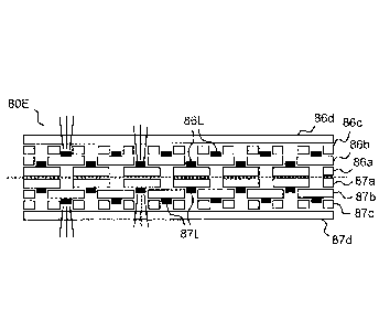
Figures 6a¨c illustrate further embodiments regarding the connection of layers
with a plurality of pins. The holes for the pins in the plastic layer may have
different
shapes. Figure 6a shows an inner design option for a pinhole 63 shown as a top
view. The left-hand side of the pinhole 63 includes a sub-part 62a which is
benda-
20 ble. When the pin 64 is inserted in the pinhole 63, the sub-part 62a
will bend
downwards, ensuring an electrical connection between the pin 64 and the corre-
sponding layer 61a with the sub-part 62a. Conducting wire 60a is illustrated
as a
horizontal thick line on which the pinhole 63 also locates.
Figure 6b illustrates the stacked group of layers 61a-61d with each having a
pin-
hole 63, and the pinholes have been aligned along the same line. The pinhole
for
the top layer 61a has a bendable sub-part 62a on the left-hand side of the
pinhole.
Instead, the pinhole for the second layer 61b from the top has a bendable sub-
part
62b on the right-hand side of the pinhole. Conducting wires 60a, 60b are
present
in layers 61a and 61b, respectively. When the connecting means, such as a pin
64, is inserted into the aligned group of pinholes 63, the connection is
achieved in
this case between the conducting wires of the two uppermost layers 61a, 61b.
With such a connection arrangement, different layers can be electrically
coupled.
An example of such a connection is shown in Figure 6c with the pin 64 and its
fix-
ing counterpart 65 in their places. The pin 64 and the near-by locating parts
of the
CA 03028575 2018-12-19
WO 2017/220847 PCT/F12016/050450
21
stacked layers 61a¨d are shown as a side-view of the pin, as a vertical cross-
section in Figure 6c. In this structural embodiment, electrically conductive
patterns
of selected layers of the same module and/or adjacent modules can be
electrically
coupled between one another. In Figure 6c, the uppermost layer 61a of the left
screen module has a sub-part 62a towards the left-hand side of the pin 64, and
this layer comprises the conducting wire 60a. The second uppermost layer 61b
has a sub-part 62b bent towards the right sidewall of the pin 64, and this
layer has
the conducting wire 60b. Layers 61c and 61d are here non-conductive layers. In
this way, two uppermost layers 61a, 61b have an electric coupling to the pin
64
and thus, the two uppermost layers 61a, 61b have an electric coupling to one
an-
other, but the other layers 61c, 61d are not electrically coupled to either of
them.
It is possible to use a conductive adhesive material, such as conductive glue,
be-
tween the conductive pin 64 and any layer with the conducting wire 60a, 60b,
in
order to enhance the electrical coupling between these two elements.
In case different layers of the same module are coupled together with the pin
con-
nection method discussed above, the pinhole such as the one shown in Figure 6c
may locate on any part of the inner surface of a module (i.e. not necessarily
on the
edges of the planar layers). In case two adjacent modules and their layers are
coupled together, the pinhole preferable locates on the seam area of these two
modules (i.e. on the edge of both modules). With such a connection method,
there
are significant advantages because the connectivity between different modules
makes the system very scalable in its size. Also the thickness (number of
layers) is
largely scalable. These aspects result into the fact that the size and the
resolution
of the screen can be varied a lot in view of the used application.
Also, connecting means such as pins can be made of a non-conductive material,
where the connecting means physically connect the at least one module with the
frame structure.
As an example referring back to the embodiment shown in Figure 4a, the connect-
ing means may be used to connect the layers 41a and 41b together.
Alternatively,
the connecting means can be used to connect the layer pairs 41a, 41b and 41c,
41d together, when creating the 4-layer structure from the 2-layer structures.
A fur-
ther option is to combine the finished modular pieces together with the
connecting
means, no matter how many layers the final screen structure module comprises.
CA 03028575 2018-12-19
WO 2017/220847 PCT/F12016/050450
22
Figures 6d and 6e show two examples where the layers are connected to a frame
12. In Figure 6d, a single module with four layers is fixed to a frame section
by a
plurality of pins 64. At first, the four layers can be fixed together by
placing the lay-
ers between the pin 64 and its counterpart 65. Then the counterpart 65 can be
at-
tached to the section of the frame 12. The pins 64 can reach into the frame
12, in
order to enable the possible electrical conductivity between an internal
signal wire
within the frame 12 and at least one of layers through the conductive pin 64
(as
discussed in connection with Figure 6c). Of course, the number of layers can
be
selected freely, and also a single layer can be fixed by this way onto the
frame 12.
The structure of Figure 6e fixes two adjacent four-layered modules onto the
frame
12 by a plurality of pins 64 in the seam area of the two modules.
Figure 6f illustrates examples of connecting two modules with a pin and
adhesive
glue. The left-hand side image shows two modules 66a¨b, one module 66a above
and another module 66b below the horizontally directed pin 67a. The pinhole is
made in both modules 66a¨b and the pin 67a can be attached through the hole. A
counterpart 67b can be used in fixing the connection with the pin 67a.
Adhesive 69
such as conductive glue can be placed between the modules 66a¨b and the pin
67a, and the adhesive acts as a reinforcing means for the location of the
connec-
tion, and also for enhancing the electrical coupling between the modules. In
the
right-hand side image of Figure 6f, the end sections 68 near the seam of the
mod-
ules 66c¨d are folded along the sides of the pin 67a. The gaps between the
folded
module end sections 68 and the pin 67a can be provided with conductive glue
69.
The pin 67a can also be some other connecting means, such as a screw, a stud
or
a crimp connector. The cables and conductive wires within the frame structure
can
be placed in contact with the conductive wires or patterns of the modules
through
conductive pins and with conductive glue assisting in the contact points.
Further-
more, a module may be connected to the frame structure also in somewhere else
than in their seam area. In case there is no need for electrical coupling, the
pin can
be an electrically non-conductive pin.
Figure 7 illustrates an example of a printed electrically conductive pattern
achieved
through a multilayer structure and showing the above pin-mediated connection
lo-
cations. Pin connection locations are shown as 71 along the circuit pattern.
The
rest of the patterns form the desired circuitry applied in the selected use of
the lay-
ered screen structure. The large square-shaped areas between the thick
vertical
wires are holes which are meant to be aligned with the LED part of an adjacent
CA 03028575 2018-12-19
WO 2017/220847 PCT/F12016/050450
23
layer, as discussed earlier e.g. in connection with Figure 4a. Figure 7
illustrates
circuitry used in this particular example, and the white area below the
illustrated
pin connection locations represent the space reserved for the LED.
Different application areas and desired layer structures are discussed next in
con-
nection with Figures 8a¨e. In a first example of layered structure with
designated
functional layers, there is a 3-layered structure comprising a LED layer 81,
solar
panel layer 82, and a battery layer 83. The battery layer can preferably be a
re-
chargeable battery. Such a structure 80A is shown as a simplified structural
image
of Figure 8a. Depending on the selected application, the LED layer(s) 81 act
either
as screen means or illumination means. The LED layer 81 is made of transparent
material. Beneath the LED layer there is the solar panel layer 82, which
receives
solar energy in an almost uninterrupted fashion because of the transparency of
the
above placed LED layer. Beneath the solar panel layer 82, there can be one or
several battery layers 83. In the Figure 8a, there is a single battery layer
83. The
structure 80A of Figure 8a is capable to show visual information and/or
illumination
and collect and store solar energy which can be used as energy supply. In this
case, the LED layer 81 points to the outwards direction if this structure is
used e.g.
in a window. The circuitry details and electric supply wires are of course
missing
from this simplified illustration.
The application areas of the structure 80A according to Figure 8a comprise
appli-
cations where the screen is placed on a fixed wall, or on other non-
transparent ob-
ject. Various signs, guiding means and information providing means such as ad-
vertisement screens with either static or dynamic image information are
possible.
One possible option is to place the structure on a planar or curved object
surface
where the object might be formed from hard plastic which is injection molded
into a
desired shape and which can be provided with embedded circuitry and the screen
sections formed by the present invention. Hybrid systems are a useful
application
area in this regard, and more details for these kinds of systems are disclosed
later.
In the structure according to Fig. 8a and also the structures disclosed in the
follow-
ing, it is possible to neglect the battery layer, and use the screen or
illumination di-
rectly from the energy achieved through the solar panel. In an alternative
embodi-
ment, an external battery may be connected to the structure, which is used to
store and provide the electrical energy to the device.
Generally speaking, instead of a single battery layer, there can be also
several
separate battery layers used in the single screen or illumination structure.
CA 03028575 2018-12-19
WO 2017/220847 PCT/F12016/050450
24
The solar panel layer may be manufactured with patterned (shaped) active
regions
collecting light energy, and the active regions may be manufactured on a
polymer
film.
In Figure 8b, a double-sided screen structure 80B is illustrated as a
simplified
structural image. This structure has six layers. In this example, there are
two sepa-
rate screen structures which coincide with the structure of Figure 8a, meaning
that
both structures have three different functional layers 81, 82, 83 stacked on
top of
each other. In the second example of Figure 8b, another of these structures is
flipped around 180 degrees and stacked on top of the other structure so that
the
battery layers 83 will be placed on top of one another. In this way, a double-
sided
screen structure 80B is created, where the layers from the top to the bottom
are:
81, 82, 83, 83, 82 and 81. LED layers 81 form the outer surfaces of the
structure,
and they enclose the rest of the layers between them. Such a structure is
capable
to collect solar energy from both sides of the layered structure and
simultaneously
display image information to both sides of the structure, resulting in a dual-
sided
display.
In the double-sided application of the screen structure, the two displays may
be
controlled so that either one of the displays works at a time, or both
displays work
at the same time.
The application areas of the two-sided display are various. They can be used
for
instance in two-sided traffic signs, information signs or even traffic lights.
Two-
sided displays can be placed in or on top of transparent surfaces such as
window
glasses. In public outdoor use, the benefit of having a dual sided solar panel
is re-
alized when applying the display e.g. for transparent walls of a bus stop.
Figure 8c illustrates a further embodiment for the screen structure 80C, where
the
light energy can be gathered from a first direction and the visual display
infor-
mation is shown to a second direction, where these directions are 180 degrees
opposite to one another. This type of structure can be used like a rolling
shade in a
window. In such a structure, the first layer is the LED layer 81, the second
layer is
battery layer 83 and the third layer along the stack is the solar panel layer
82.
When this screen structure 80C is placed e.g. on an outer window of a
building,
with the solar panel layer 82 pointing outdoors, a beneficial arrangement is
achieved. The solar energy can be gathered directly because the solar panel
layer
points outwards to the ambient environment. The LED layer 81 will then provide
the visual information or illumination internally within the room or space
supplied
CA 03028575 2018-12-19
WO 2017/220847 PCT/F12016/050450
with the window and the attached screen. Such a structure 80C enables visual
screen means without any need for external wires from an external electric
supply.
Furthermore, regarding the application areas which can be used in a form of a
roll-
ing shade, there are several different structural possibilities for the layers
forming
5 the screen. The actual screen structure layers comprising the LEDs may be
incor-
porated in the window or on the window surface. In this embodiment, the screen
structure with the energy gathering and storing means can be divided in two
differ-
ent elements, which are connected to one another. During daylight time, the
rolling
shade comprising at least the solar panel and the battery layers can be pulled
10 down on the window, in order to let the solar energy to be captured by
the solar
panel layer. During the night time when the daylight is absent, the screen or
illumi-
nation functionality can be turned on in the window in order to show a desired
dis-
play content or alternatively, to switch on a illumination element which acts
as a
rectangular LED-based light source in the window. The battery and solar panel
15 layers may be in a rolled state during the night-time, just like the
regular rolling
shades are normally during the daylight. Such a night-time functionality also
does
not let anybody from the outside to see through this window, ensuring privacy
for
the people inside the building, whether in private or office or other public
use. The
window discussed above may also be other kind of a transparent wall which may
20 locate also in a non-vertical direction. Such a illumination arrangement
is a cost-
efficient manner to use solar energy for illuminating interior (regular
window) and
also exterior spaces (transparent wall outdoors). As an alternative or as an
addi-
tion to illumination purposes, such a structure acts as a cost-efficient
screen for
e.g. advertisement or guiding purposes.
25 As a further option, the energy collected in the battery layer(s) of the
screen struc-
ture through the solar panel layer(s), can be used to other devices,
appliances or
illumination devices locating e.g. in a nearby environment. For instance, the
screen structure can be installed into a window of an office, while all or
some of
the other office lights may be supplied with the collected solar energy from
the
screen structure in the window.
As a further option regarding the structure of the different layers, it is
possible to
place the solar panel layer as the outermost layer. Of course, an additional
protec-
tive layer can be set as a coating to the solar panel layer. The LED layer(s)
may
then locate under the solar panel layer. The solar panel layer may be
patterned in
order to achieve a display on a façade of a building, a design object for
household
CA 03028575 2018-12-19
WO 2017/220847 PCT/F12016/050450
26
use, or a sun shade e.g. placed on top of an entrance or window. The result
can
be a surface or object in public or private place where the solar panel with
the
screen (or a light) can be shaped or patterned unnoticeably on top of the
structure.
The screen or illumination device structure according to any embodiment of the
in-
vention can be implemented in a printed hybrid system. This is achieved by
injec-
tion molding of an object. The materials used here can be various, and synthe-
sized materials such as plastic is a beneficial material in such applications
be-
cause it can be used to create freely selectable support structures and forms
for
electric devices and the circuitry needed in them. In some applications,
transpar-
ent plastic material such as acryl is of great use. In hybrid structures,
printed pat-
terns and sub-parts can be combined with traditional electric components. The
printed hybrid system can apply wireless and loT ("Internet of Things")
connectivity
means. All the various structural embodiments from the above disclosure may be
applied. Alternatively, connectors for the external data transfer and/or
current sup-
ply may be provided as an alternative or additional means for the wireless com-
munication and for the possible internal power system such as a solar panel
and a
battery discussed earlier. Furthermore, specific sensors or e.g. an optical
camera
can be placed in connection with the screen or illumination device. Generally,
the
layered structures can be shaped and/or fixed in desired 3-dimensional shapes
which is a great advantage. Also the integration of electronics into e.g.
shaped
plastic structures results in a robust, well-protected device which can be
made al-
so in a compact size if needed. Maintenance is also easier because the whole
de-
vice is integrated into a single physical entity. Possible applications are
incredibly
various, like e.g. consumer electronics, car technology, traffic signs,
traffic lights,
information boards and medical diagnostic devices. Also decorative uses are
pos-
sible for interiors and exteriors, and various design illumination products
and also
illumination arrangements used in arts are possible.
Further application areas relating to the hybrid systems comprise household
and
office design illumination devices or other household electronics devices
which
may have very special forms compared to traditional illumination fixtures and
de-
vices. For instance, veneered structures can act as an installing platform of
a flexi-
ble layered screen module where the veneered structure may have holes or cavi-
ties where the LEDs are designed to locate. As one optional design, the screen
structure may be placed along a desired surface made of wood where the LEDs
point outwards from the surface. The size of the screen structure may be
selected
so that the input supply current to the illumination device can be connected
to the
CA 03028575 2018-12-19
WO 2017/220847 PCT/F12016/050450
27
supply wires of the screen structure. The screen structure can then be covered
with a protective layer where the LED locations are either free (provided with
holes) or the protective layer on the LED locations is transparent. In this
way, the
design is more robust and also more aesthetically pleasing.
In general, the flexible screen structure according to the invention can be
imple-
mented with wood-based structures or objects, instead of synthesized materials
like acryl or other plastic materials presented earlier. In this way, designed
illumi-
nation devices for interiors and exteriors, household furniture, electrical
appliances
and the like, and pieces of art can be implemented with the structures
according to
the invention. Also illumination and display arrangements in various cultural
or en-
tertainment venues and applications is possible, e.g. for stage lights of a
theatre,
or display arrangements in an escape game room, just to present a few
examples.
A further embodiment is shown in Figure 8d. This arrangement illustrates a two-
layered structure with double-sided screen. The first layer 84 is the top
layer and
the second layer 85 lies beneath the first layer 84. Both layers are provided
with
holes placed within uniform distance from one another. The diameter and shape
of
the hole is selected so that a LED component can be placed at least partly in
a
hole. In other words, the size of the LED is slightly less than the size of
the hole so
that a LED can accommodate a corresponding hole, like a piece in a jigsaw puz-
zle. The two layers are provided with attached LED components, with the same
mutual distance within one another as the above defined hole distance. When an-
other layer is flipped 180 degrees around a horizontal axis, the two layers
can be
placed together, with LED components adjusted in the holes of the other layer.
The LEDs attached to the first layer are LEDs 84L, pointing downwards in
Figure
8d. Correspondingly, the LEDs attached to the second layer are LEDs 85L, point-
ing upwards in Figure 8d. The resulting structure has very little attenuation
regard-
ing LED light emittance because there is no plastic layer in the emitting
direction of
a LED. Also the structure is a robust one because of the jigsaw puzzle type of
ad-
justing of the two layers. This is also a simple structure to achieve a dual
screen
functionality.
In yet another embodiment of the invention, the structure of Figure 8d can be
transformed so that the second layer 85 is flipped around a horizontal axis
180
degrees and the layer with LEDs pointing downwards can be placed in top of the
first layer 84, with LEDs 85L placed in the holes of the first layer 84. In
this way, a
one-sided screen or illumination structure with doubled resolution can be
manufac-
CA 03028575 2018-12-19
WO 2017/220847 PCT/F12016/050450
28
tured. In a further embodiment, such a two-layer structure can be doubled so
that
another 2-layer structure points its LEDs in the opposite direction compared
to the
first 2-layer structure. In this way, an efficient dual-sided screen or
illumination
structure can be created. Finally, the number of layers can also be greater
than
.. two, in order to create a multi-layer structure for a single viewing or
illumination di-
rection (or twice that amount for a dual-sided screen or illumination
element). Addi-
tional layers described previously in the description may be used in addition
with
the active layers with LEDs.
The previous dual-sided embodiment is illustrated as a four plus four layer
cross-
.. sectional example in Figure 8e. Layers 86a and 86b are stacked on top of
one an-
other so that LEDs 86L on a first layer 86a are placed in a hole of a second
layer
86b. The second layer 86b is topped with an additional layer 86c where the
LEDs
86L on the second layer 86b are placed in the holes of the additional layer
86c. A
transparent protective layer 86d is placed on top of the stacked layers to
protect
.. the LEDs and the structure in general, resulting in a 4-layer structure for
a single
viewing direction. Thus, all LEDs 86L have direct visibility because the only
layer
required to be penetrated by the light of the LEDs is the protective layer
86d. The
4-layer structure 86a¨d is doubled so that the second 4-layer structure 87a¨d
is
flipped 180 degrees around a horizontal axis and attached on the back side of
the
first layer 86a. The line showing the attachment area between the two 4-layer
structures is shown as a dashed line. The LEDs 87L thus point in an opposite
di-
rection than the LEDs 86L, when the arrangement is in a planar form. Also the
other layer structure is topped by a protective layer 87d. The number and
types of
any intermediate layers can be freely selected. Also the number of LED layers
for
.. a single viewing direction can be one or more than two, as it has been
disclosed in
earlier described embodiments.
A yet further embodiment of the invention, and actually an application area
for the
presented screen or illumination arrangement is a screen or illumination
device
which can be placed below a layer of ice. This means that the screen structure
.. with a single viewing direction can be placed on a fixed platform, such as
on a
concrete layer. In the ice application, the polymer layer or layers of the
screen
structure can be non-transparent, because the structure lies on a concrete or
other
solid base. There might be holes for the LEDs and even some additional holes
in
other parts than the LED locations of the structure in order to enable matter
such
.. as water or remaining air under the screen structure to flow through the
screen
structure in order to enable the water and/or air to exit the structure before
the
29
freezing takes place. This helps to make the structure as smooth and planar
without any
air bubbles trapped within the structure, thus easing the laying of the good-
quality ice layer
on top of the screen structure. The LED layer(s) need to be provided with a
protective layer
in order to prevent any water to enter into the structure. The screen
structure acts as a
platform for a next layer which may be an insulating layer. On top of the
insulating layer,
there can be a cooling layer for the ice. As an alternative solution, the
cooling layer locates
in the bottom within a concrete base, and the LED layer(s) are placed on top
the cooling
layer, without any insulating layer. In that way, the cooling will have an
effect through the
LED layers into the ice placed on top of the whole structure. Ice layer will
be set on top of
the final layer structure. In one embodiment, the screen structure can be
located within the
ice layer so that the distance of the screen structure from the top surface of
the ice can be
selected to enable the best view of the screen through the ice. The holes in
the screen
structure also help the cooling of the ice layer. The resulting effect is a
screen or an
illumination arrangement visible through ice.
In one embodiment of the ice application, the temperature of the ice layer can
be measured
and in case the temperature is above a given threshold value indicating a
melting possibility
for the ice, the control system of the screen structure can control and manage
the output
power fed to the LEDs. This enhances the quality of the ice through cooling
the ice layer
well under the threshold. The threshold can be slightly below 0 degrees, as
an example.
In one embodiment, the screen or illumination structure may comprise a sensor
layer using
e.g. temperature sensors used to measure the temperature, or optical sensors
used for
visual inspection of the quality of the ice.
In one embodiment, which has benefits especially in temperature prone
environments such
as ice rink screens, the LED locations of the screen structure are covered by
plastic bubbles
formed in the protective layer. The plastic bubbles act as protective elements
for the LEDs.
The plastic bubbles may also help in drifting the thermal peaks of the
structure in a more
distributed manner across the screen structure.
The applications comprise different ice-covered arenas, such as ice hockey
rinks. All the
required lines and markings for the ice hockey games might be created through
the ice-
integrated screens. Also, it is possible to create various other lines and
field limits for other
sports than just e.g. ice hockey, in a multi-sports venue. This also applies
for any indoor or
outdoor sports field without any ice. Further-
CA 3028575 2019-03-22
CA 03028575 2018-12-19
WO 2017/220847 PCT/F12016/050450
more, the screens can be used in creating fixed or modifiable advertisement
spots
visible through the surface of the ice. The modifying capability of the
created ads is
a great advantage because there would then be no need to remove the ice when
there is a need to change advertisements beneath the ice. Of course, the
princi-
5 ples of the invention are well suitable to all other locations available
in a sports
venue, such as for guidance or advertisement means on the walls or windows or
dedicated information screens in a sports arena, or as a main or additional
result
board within the venue or e.g. on rink walls or within a plexiglass
surrounding the
ice hockey rink. The options in this regard are plentiful.
10 Regarding the embodiments below a solid transparent material layer such
as ice,
the solid ice layer also acts as a diffusor element for the light sources.
This means
that single LEDs are not that easily visible farther away from the screen
structure.
Regarding the desired quality in the created images in the display, this might
have
an effect to the LED resolution within the screen structure, or to the
thickness of
15 the transparent solid material on top of it.
Generally speaking, the layers of the structure can be selected from this
group of
dedicated functionalities: a LED layer, a solar panel layer, a electrically
conductive
pattern layer, a battery layer, a holed film layer, a physical support layer,
a protec-
tive layer, a thermally conductive layer, a thermally insulating layer, a
diffuser lay-
20 er, a reflective layer, an electroluminescent emission layer or a sensor
layer com-
prising dedicated sensors. Sensors may comprise optical sensors, movement
sensors and/or temperature sensors, for instance. In one embodiment, the
optical
sensors can be implemented in a form of a camera.
Summarizing different possible options in using the presented structure, the
appa-
25 ratus is used in printed hybrid systems, in architectonic media surfaces
such as in
or on a transparent glass or polymer wall, on a non-transparent wall, ceiling,
floor
or other planar or curved surface, in injection-molded elements or devices, in
wooden or veneered structures, below an ice layer in ice rinks, in sports
fields or
arenas, in traffic signs and lights, in public transportation vehicles such as
buses
30 and trains, in guiding signs, advertisement arrangements, in decorative
purposes,
in a furnishing element used in a household or in public premises, in
illumination
devices, in loT (Internet of Things), as a rolling shade on a window, in
artistic pur-
poses, in cultural and sports venues, in activity parks, theme parks, playing
fields
for children, in educational or business presentation purposes, or in gaming
or en-
tertainment applications.
CA 03028575 2018-12-19
WO 2017/220847 PCT/F12016/050450
31
The screen or illumination apparatus can be placed in a non-planar arrangement
when it is manufactured or set in its position for use.
The inventive idea comprises also a corresponding manufacturing method for
screen or illumination apparatus. The manufacturing method comprises the steps
of:
¨ manufacturing at least one LED layer (41a¨d, 51a¨e, 61a¨d, 81, 84, 85,
86a¨b, 87a¨b), each LED layer comprising a plurality of LEDs (43a¨d, 52, 84L,
85L, 86L, 87L), where at least one LED layer is at least partly made of a
polymer,
¨ where each single LED layer comprises electrically conductive patterns
(60a-
b), where the LEDs are electrically coupled with the electrically conductive
pat-
terns,
¨ creating a layer arrangement for a single module (11, 20) by stacking the
at
least one LED layer and possible other layers in a desired order, and
repeating the
creating step in case of a plurality of modules are desired; and in case at
least two
modules (11, 20) are formed,
¨ connecting the at least two modules (11, 20) together in order to form
the ap-
paratus.
The manufacturing method can be implemented partly or fully by a computer pro-
gram which is executable on a processor or other computing means. The connput-
er program comprises code and it may be stored in a computer-readable medium.
In one embodiment, it is possible to place at least one other layer within the
LED
layer arrangement; i.e. a non-LED layer may be placed between two LED layers.
Therefore, the LED layer arrangement can be a distributed group of layers
within
the whole layer structure. As a summary, the order of LED and non-LED layers
may be freely selected among the layer arrangement.
The advantages of the invention are various. The structure is a modular one
where
the module size is freely scalable. The number of layers and the LED density
with-
in a module can be freely selected based on the used application. As a
practical
advantage relating to the movability and size of the apparatus, the layered
screen
and illumination apparatus is rollable into a rolled form for easier transport
and
storage purposes. Also the installment of the device to the desired location
is easy
from the rolled screen elements. Furthermore, the roll-to-roll method enables
a
cost-effective manufacturing process if desired.
CA 03028575 2018-12-19
WO 2017/220847 PCT/F12016/050450
32
Furthermore, the structure can be installed in various non-planar shapes
because
the material is flexible. The sizes of the display or illumination device is
highly
scalable for different purposes, allowing very large screens for public use
and very
small screens e.g. in a wristwatch type of a device. Because the base material
is
.. polymer, the screen and illumination structure is thin and light-weighted
compared
to traditional screen structures. Furthermore, polymer can be selected as
trans-
parent, and by adding holes to the structure, the transparency can be enhanced
even more.
The layered structure with thin layers enables the heat to be managed more
easi-
ly, in order to direct the emerging heat out of the structure.
Different embodiments disclosed in the dependent claims and in the details
above
may be combined with one another in order to achieve a new embodiment of the
invention.
The present invention is not limited to the above presented embodiments but it
may vary within the scope of the claims.