Note: Descriptions are shown in the official language in which they were submitted.
1
TITLE OF THE INVENTION
A system and method for bidirectionally based electrical information storage,
processing and
communication.
TECHNICAL FIELD
The present disclosure is generally related to semiconductor memory storage,
and more
particularly, is related to dual polarity memory systems and methods for
storing, retrieving, and
processing tristate interpretable information.
BACKGROUND
The foundation for information processing, and modern computing, has been our
ability to observe,
store, and alter, information. In electronic systems, the systems that store
this information are
called memory. Memory refers to the ability of physical systems to generate
electronic signals,
principally analog, that may be routed, controlled, altered, and stored, to
allow for later use, and
recall. The general concept of memory, and the language of electronic
computation, and
communication is binary, meaning a language utilizing ones and zeros based on
the charge state,
and or switch position of a physical memory system.
Information is stored on physical systems, then processed from memory for use
with additional
systems. The design of our information processing systems is unidirectional,
meaning current
travels in a single linear path. This design includes the way in which we use
and store information
on physical memory systems, that being charging memory cells in a single
forward bias, and or
turning a switch on or off when operating in the binary framework. The premise
of storing
information is by utilizing transistors, and or transistor capacitors pairs,
to store information in either
a 1, signifying a charge or active state, or a 0, signifying a no charge or
inactive state. This single
state change is the foundation for most computer operations, and is referred
to as bits of
information, binary being the name of the language that creates a designable
framework for
computers to interpret specific bit patterns into words, statements, and
logical functions, as well as
operations and programs.
The success of this design, and operating language framework has allowed the
massive adoption
and success of computing, as well as information processing. This has led to
continuous high dollar
value investments, which has allowed for the continued advancement and
complexity of these
systems, resulting in the ability to fit more electronic components into
smaller and smaller systems,
reducing size, which has followed the widely accepted Moore's law.
CA 3030723 2019-01-21
2
There have existed competing methods of information processing, specifically
ternary and
quaternary, that never saw the commercial success of binary. Though these
competing systems
offered many benefits, the simple use and operation of binary allowed the
massive adoption of
this information processing framework and resulted in the competing
technologies becoming
lost to the history books, and obscurity.
Summary
Technical Problem
The technical problem is the limitation imposed by the defined two-state bit
position constraint,
and single bit (Shannon) storage operation, for a single memory cell, and in
turn a computer's
computing abilities while operating traditional memory systems, specifically
for this disclosure
DRAM "dynamic random-access memory".
In order to operate a DRAMs structure as well as its functionality there is a
standard
"framework" that is required including: sense amplifiers, repeaters, logic for
refreshing the
contents of the DRAM, as well as bit-line and word-line selectors, block
selectors and additional
systems, some of which are included in the description to further describe the
invention, while
others have been omitted for simplicity.
Computation is based on traditional information processing and memory storage,
a rigid
framework of single bit information encoding, that resides in one of two value
states i.e. 2Nt1
bits. The challenge presented, is due to the fact that information is stored
within memory
systems as one of two values, the first value being a 0 or off state, the
second being a 1
signifying a charge present, and as an on state. This results that memory
storage, and
computation, is based on memory cells with a single bit (single Shannon) of
actual information
being stored per cell. This binary framework results in, when attempting to
solve technical
problems, for instance when exponentials are presented, a rapid growth of
variables required
for computation, and therefore memory storage spaces required to complete the
operation. This
exponential growth of required memory currently surpasses the abilities of our
state-of-the-art
memory systems, and processing capabilities. The compounding nature of
exponentials causes
our current technology, specifically our ability to compute these large sums,
to very quickly
reach our limitations, leaving many questions unanswerable, and operations
unable to
complete.
Additionally, the application of memory in physical systems has required that
the information that is
stored can only be expressed in one of two possible states, and where it must
always be in one of
Date Recue/Date Received 2024-03-11
3
these two states at any given time. That being either on or off, representing
either a 0 or a 1,
signifying one piece of retrievable information.
This is the constructed framework of our current memory systems, that lays out
this mandatory
information encoding requirement, meaning that in every memory system, one of
these states must
be active. That a single piece of the physical memory must at all times retain
one of these two
states of information, and at the same time can only hold this one piece of
information. This
includes even when the system is off (no power), and when no power is present
the system would
hold all states at 0, specifically with dynamic, or short-term memory.
The challenge with having to have one of these two states always representing
one single piece of
information is that it takes multiple single pieces (bits) of information to
actually form a usable
statement, and or meaningful and usable information. With the initial 8 bits
(8 memory cells)
forming a single character known as a "word". Being held to this single piece
of information per bit
0/1 on/ off, means that the ability to form complex variables requires large
quantities of physical
memory systems, each holding a single piece of information. This causes
challenges when solving
complex problems, when a determination is required that encompasses a sequence
of numbers
longer than what can be stored as bits on physical memory. Even though we can
build systems
with trillions of these bits, we still utilize a framework that makes many
problems unsolvable.
Additionally, when investigating alternative information processing and memory
systems,
specifically ternary, the challenges associated with utilizing this
information processing method
have not been overcome, and as such have not led this processing framework to
be able to form a
viable commercial presence to date. To understand ternary computation, it is
important to
understand that this type of information processing is an entirely separate
method of interpreting
and storing information.
Ternary is a language based on a base multiplication and factorial of 3, 3Nth
bits. Meaning as
opposed to binary where information is stored in one of two states (0, 1),
ternary is stored in one of
three states, which may additionally be represented in a few different
methods. For instance, one
method is unbalanced, and the three states are represented as (1, 2, 3) which
may also be (0, 1,
2). The next method is balanced, and the three states are represented as (1,
0, -1) or (10, 00,01)
which may also be seen as only polarity symbols (+, 0, -). Though a working
and operable
computer was developed by the Soviet Union in 1958 called "Setun", the
commercial sales of the
system where discontinued and information specifically related to its
construction and operation are
not readily available and may remain classified.
CA 3030723 2019-01-21
4
Setun was a ternary based computer that utilized a rotating drum for memory
storage, this drum
could be operated in a similar manner to the disclosed system and method, that
being
bidirectional based memory charging. The operation of the device was more
limited, due to the
operation and physical size of the drum, used as the dynamical random-access
memory, but did
allow the storage of more information for each memory cell. This bidirectional
memory design
demonstrated at the time that construction of computers based on the Setun
design was
cheaper than the binary construction design, and additionally more robust.
This design allowed
for the information instruction, and operating language known as ternary, or
the ternary
operator.
It is unclear as the reason that ternary was not adopted, and binary became
the predominant
operating language. My belief is that at the time the basic simplicity of
binary allowed a much
larger percentage of developers to learn and understand binary's basic
premise, and operation.
This resulted in a fundamental clash of operating system language, design, and
construction
parameters, between binary and ternary computers both for software as well as
hardware. And
because generally simpler systems, that more people understand, will cause a
more rapid
growth and advancement of the system and technology, binary being easier to
understand
caused developers to gravitate to its use and development. As such the obvious
winner has
been the binary system, and the Setun and resulting ternary operator system
has fallen, and
become information stored in the history books.
There are benefits and drawbacks when using ternary as an information
processing framework,
one is the exponential growth of different possible information state
arrangements, due to three
possible information states per memory cell. This three-state system allows a
larger amount of
combinations of these three states, more combinations of symbols, for the same
amount of
memory cells that a binary system uses. Conversely you can also represent the
same amount
of combinations that 8 memory cells in a binary architecture (2 states per
cell), in as little as six
memory cells with a ternary representation (3 states per cell). The basis for
binary is the 256
possible arrangements of O's and is for each 8 memory cells, where each
different
arrangement specifies a specific character called a "word", where the first
256 arrangements
can be viewed as a legend with the standard being the ASCII Table.
Ternary on the other hand utilizes three pieces of information "states" as
referenced above for
interpretation and allows in the first 6 memory cells a total of 729 different
configurations, or
different patterns, or 3Nth bits. And since the patterns include an additional
character the two
languages are fundamentally different, they can be translated like two
different dialects, but the
individual patterns are not universally interchangeable. The Setun for
instance utilized a magnetic
drum with different polarizations to accomplish storing and retrieving each of
these three states
Date Recue/Date Received 2024-03-11
5
from memory. The challenge with trying to incorporate the ternary framework to
benefit binary
systems is that these are two separate languages for information interpreting,
and processing
systems, and as such they are structurally different.
The only way to communicate the information from one framework to the other is
by converting
"translating" the information back and forth i.e. from binary to ternary and
then from ternary to
binary as one scheme attempted to do referenced in patent number US 5,432,735.
The main misunderstanding with regards to the ternary system is that more
information is stored
per physical memory information cell, called a trit. This is not in practice
how this system works, a
single memory cell only holds a single piece of information, one bit (one
Shannon). Where the
system gains its advantage is by using the combinations of the three possible
information states,
this allows a legend of all of the same binary words represented in six memory
cells instead of
eight. In order to benefit from the ternary framework, you must utilize the
ternary character legend
for information processing.
The disadvantage this presents is that the information processing of these two
systems are
fundamentally different, where you can interpret back and forth between the
two "languages" for
lack of a better analogy, but they are fundamentally non-integrateable,
without utilizing the ternary
language framework, and hardware operational systems, you do not gain the
benefit of 3Nth bits of
information. This is because both existing traditional binary, and ternary,
memory cells only store a
single piece "bit" (Shannon) of information, though representing either two
information states in
binary, or three information states in ternary.
Solution to technical problem
The solution to the technical problem is utilizing a bidirectional based
memory system, that may be
additionally constructed and interconnected 3-dimensionally. This allows for a
wider range of
computation based on a more flexible information processing framework, and in-
turn store more
that a single piece "bit" of information per component "cell" of a memory
system. Bidirectional
memory offers the capability to store more information per cell, and per
component, rather than two
possible states, and a single bit of information per physical memory cell.
This benefit is additionally
realizable in the binary framework and language when not assuming it must
exclusively bound to a
ternary computer, or ternary language framework.
There are multiple benefits to the disclosed system and method, and these
include; the ability
within a binary and or ternary framework to store more information per
physical memory system.
The ability to set a distinct meaning for each additional information
statement. The ability to access
CA 3030723 2019-01-21
6
multiple pieces of information per system (cell). The ability to allow each
piece of memory to be
expressed as a state of constant variability (superposition). The ability to
form more complex
systems for information storage, compression, and processing. The ability when
solving
computational problems to eliminate more possible outcomes for each piece of
information attained
.. from a single memory system (cell), or plurality.
The ability to store more information per memory system (cell) is a major
improvement over
traditional system. When holding this larger quantity of information, you can
utilize a greatly
reduced amount of physical memory to preform computations and store
information, including for
the operation of computer systems, and information processors, when compared
to traditional
.. memory systems.
Summary of the Invention
The actions of computers are built from electrical signals, which work to form
information stored as
bits/ bytes, as these bits and bytes are expanded, they form sequences that
can be used to form
statements, problems, and preform actions. The binary framework and language
builds upon the
ability of memory to store a single bit of information in one of two possible
states, a zero or a one.
But though this language has been applied to act based on single bits of
stored information it can
also be applied to vast groupings of these systems, and in connection with the
speed of processing,
that may operate in the gigahertz, allows complex operations to be preformed.
This is by executing
.. statements sequentially, resulting from the ability to assemble, and
compute, many otherwise
simple tasks, in high speed succession to allow for more complex mathematical
operations.
When utilizing the binary language for information processing a basic
character statement "word"
can be developed from one byte of information. One byte is a grouping of eight
bits, and since each
bit has to be maintained in a zero, or one state allows for the possibility of
256 different zero/ one
combinations. This is accomplished through the exponential growth of possible
combinations for
each bit added to a memory system, i.e. bit 1 with 2 possible values, bit 2
with 2 possible values, bit
1 multiplied by bit 2 equals 4 possible values. If you add a 3rd bit, then you
multiply your first 2 bits
possible values, giving you your 4 possible values, multiplied by two more
possible sequential
values (3rd bit) to get a total of 8 possible values. This exponential growth
continues, so that with
.. eight sequential bits you have attained 256 possible value combinations.
The challenge with this framework is that even though you have an exponential
growth of possible
values, the information stored per memory cell is still only a single bit of
information. It would be
unmanageable to continue utilizing this exponential growth of possible pattern
configurations, the
CA 3030723 2019-01-21
7
additional bit adding to a memory cell sequence twice the amount of possible
patterns could
theoretically continue until all possible representations describing "words"
are exhausted. This
would make using this system erroneously complex and therefore practically
unusable. Instead the
benefit of the exponential growth of pattern configurations is only used in
the first 8 bits to form 256
different characters "words" (regionally this may vary generally up to a
maximum of 12 bits) to form
a legend. These individual words are then placed sequentially to form actual
readable and
interpretable words, statements, tasks, and so on, this design requires long
sequences of memory
to form statements, for instance to say "exponential" in binary would require
11 bytes and 88 bits of
information as shown "0110010101111000 01110000 01101111 01101110 01100101
01101110
01110100 01101001 01100001 01101100".Though there does exist many complex
factorial
frameworks (information trees) to allow clever compression and a reduction in
memory, this
operation and storage is the general premise, and for this disclosure will
suffice.
This framework is the largest drawback for information processing and
computing, and where a
problem has an exponential growth, and or exceeds the amount of physical
memory addresses
(cells) available in the system, renders the problem unsolvable. This
exponential growth problem is
one of the main problems that has led to the excitement and investment in
quantum computers
because of their unique abilities. Quantum computers have been designed to
operate on a different
memory framework than traditional computers, where in quantum computers
information is stored
as a qubit instead of being called a bit. Generally, quantum computers involve
utilizing the spin of
an element, for instance the spin of an electron. In some of these computers
they utilize a cooling
chamber to cool down the element to near absolute zero, causing an almost
suspended, very
inactive state of usually conductive elements, generally attempting to attain
superconductivity. Then
by assuming that the elements natural elemental spin is a spin down,
representing a 0, then if a
magnetic field is applied, where energy is used to cause an alternation of
spin to spin up,
representing a 1, you can begin the process of utilizing these devices to
store information, and for
mathematical computation. The advantage sought by the developers of quantum
computers is to
be able to utilize the spin states between spin up, and spin down, to preform
computation. The
multitude of different spin states between spin up, and spin down, allows the
interpretation that the
qubit could be in either, or any possible variation, of the states
simultaneously, this is referred to as
superposition, this definition is then interpreted to represent that there
only exists a probability ratio
of the current spin state, until measured.
This superposition concept is a great achievement in computer processing, it
allows a duality of
states, and an exponential growth in possible values. And though it allows the
interpretation of any
number of spins, i.e, 2*21\lth bits, I would argue that in information
processing it is actually only
CA 3030723 2019-01-21
8
representative of three possible states, a trit, being 0 - 1 or 1/0, meaning
that the computational
growth, of quantum computing, is a compounding exponential of three possible
information
states 3Nth bits.
In addition to superposition, quantum computers can utilize a process, and
therefor property
of qubits, to cause a phenomenon called entanglement. Entanglement is the
process of
co-synching (synchronizing) the exact spins of qubits. This synchronization
allows the
separation and observation that two entangled qubits to share the same state,
and therefore
hold the same information, and is a novel characteristic. This question of
receiving an actual
benefit is particularly relevant due to the logistical, and operational,
challenges in maintaining a
qubits entangled spin, and the transferring of this information is still
governed by the speed of
light limitation, where it could be argued the information is known, though
not observed, before
the entangled qubits are separated.
Additionally, another limitation of the operation of quantum computers is the
operational noise,
an apparent design flaw caused by the actual operation of these devices,
attributed to the
different operational systems, and the spin of the qubit. Wherein it has been
proposed that
limitations to the quantity of qubits will be inherent due to a growth in
operational noise, and
therefore limit the size and ability of these devices.
The explanation of quantum computers, referenced within this disclosure, is to
provide insight,
and context, to a few of the benefits of the disclosed system and method. The
use of
bidirectionally operable memory allows for some similar attributes to that of
quantum computers,
including additional operational abilities over traditional computing systems
that will be
discussed. To explain the operational similarities between quantum computers
and bidirectional
memory we must first begin with their similarities of operation, when in
context of the traditional
bit and binary computer language, and information processing framework.
.. Bidirectional memory, as the name describes is memory that can operate
bidirectionally,
meaning that the physical system, analog memory cell, allows the current flow,
and stored
charge operation, to be accomplished in either the forward/ positive bias, or
the reverse/
negative bias. This ability to alternate the charging bias, is accomplished
with a system of
components to allow a change in the direction of current traveling through a
storage device.
.. One embodiment of a single un-interconnected memory cell being 1 transistor
and 1 capacitor,
wherein leads of the transistors are connected to each of the leads of the
capacitor, and by
activating the transistor and by changing the voltage states on opposing sides
of the capacitor
determines the current flow through the capacitor.
Date Recue/Date Received 2024-03-11
9
Capacitors store a charge in the form of an electrostatic field, and though
many capacitors are
designed to be polarized this feature is not a requirement. Additionally, due
to the extremely low
voltages of typical memory systems the likelihood of damage or failure even
when charging a
polarized capacitor inversely is relatively low, and may be designed to reduce
this risk further,
though non-polarized capacitors are preferred.
Due to this property of capacitors, able to be charged in either a forward
bias, reverse bias, or
maintain no charge, allows this memory cell to contain more information than
in a traditional
framework, a ternary, or trit, of 3 pieces of information, and or states,
3N1th bits. Traditional
information storage as previously discussed, allows a single memory cell to be
in one of two
3.0 possible states, and hold a single piece (a bit) of information 2NIth
bits. Quantum computers allow a
memory cell (qubit) to operate one of three possible states while still
holding only a single bit of
information 31\l'h qubits. Though one embodiment of the disclosed system and
method could be
utilized in a quantum computer and framework, without going into the debate of
whether the
superposition state is representative of a single or infinite amount of
states. Bidirectional memory
also has 3 identified possible states, but due to the framework of its
operation it can store and have
retrievable information greater than a single bit of information per physical
memory cell.
Information processing is built upon this concept, and ability to
differentiate uniquely identifiable
states, that can be used to assign values and symbols, and therefore allow
logical computation to
occur. In memory systems this has traditionally been a simple on- off state of
a memory cell,
representing a 1/ 0, this information is then retrieved and stored by
additional systems within the
device.
If we choose to look at how information is processed within the binary
framework, we will see that
there exists two interpretations, and roles, the binary framework preforms
within a computational
architecture. These roles are separate, though their operations appear to
encompass the same
overall binary framework. This provides a level of camouflage making it more
difficult to separate
these roles into clearly separate, abstract operational concepts. The roles I
am speaking of are
informational processing, and mathematical computational operations, one being
word-based
information processing, and the other being mathematical computation. Though
these may seem to
be the same types of operations within the overall activities of a device they
are actually very
separate actions, even though one operation can cause an action required by
the other. For
instance, language operations are used to instruct mathematical computation,
and the results of the
computation can be displayed in understandable language.
CA 3030723 2019-01-21
10
This may seem confusing, and counter intuitive, especially considering in
order to use text each
character or "word" must be constructed of O's & l's. The reality though is
that text is just a specific
pattern of zero's and one's in the binary framework, it is simply a picture
formed by eight digits.
When you instruct a computer to preform a mathematical computation say "add 2
and 2" the
computer relays the information briefly into memory, which for this operation
may just be the cache.
Then instructs the arithmetic logic unit to preform the function and store the
information back in
memory and display the results "answer = 4". Though this operation seems like
a single seamless
operation the process is actually broken up into many individual actions, and
though the text
initiates the operation and gives task and instructions, the text does not
preform the actual
mathematical operation. Instead it is translated into the binary number
structure, and then parts of
the binary structure preform the function, for instance incrementing the
binary digits.
To provide a clear distinction and understanding of the separate roles that
language, and
mathematics, play within a computer it is important to understand that
language is only the
interpretation instrument we use to communicate with computers, and the
mathematical operations
are preformed based on binary calculations. The binary language is in turn, a
representation of both
mathematics and symbolism used for language-based interpretation. This dual
role is the same
operational system the computer uses internally, which is based on the simple
process of on/ off,
charged or not charged analog memory cells. Where each cell's information is
represented as a 0
or 1 based on this analog signal and is therefore only an interpretation. The
operation, in essence,
.. is just a complicated scratch board, and how we decide to display and
interpret these analog
signals, as visual and processable information is at our discretion.
This flexibility is why ternary has multiple options and structures for
interpreting the 3 states (31Nth
bits) of each analog memory cell, based on three analog states, positive
polarity, negative polarity,
and no charge.
If, as in the disclosed system and method, we choose to exploit this property
of altering the way in
which we visualize and recognize the analog signals we receive, and store,
within our memory
structures, we can manipulate this information to be used in new innovative
ways.
For instance, in the disclosed system and method I am introducing a
bidirectional dynamic random-
access memory cell structure, this allows charging the cell in positive
polarity, negative polarity, or
have no charge present. This type of memory has been traditionally called
ternary, and therefore
without converting between ternary and binary, it did not present benefits
within the binary
framework, and as a result has not been exploited within the binary language,
and framework. The
reason for this is that because ternary and binary are separate languages,
they interpret the analog
CA 3030723 2019-01-21
11
signals into different graphical symbols and representations, as well as there
is different internal
hardware required for operation.
The disclosed system and method allows an additional separately identifiable
signal, a negative
polarity signal, to be used within the binary framework, as well as in some
embodiments utilized
within the ternary framework.
This is accomplished by choosing the representative symbol(s) we choose this
additional analog
signal to represent. Then integrating the additional hardware required to move
the information into
and out of each memory cell, so that the CPU "central processing unit" and
subsystems can
interpret, differentiate, and process this different information state.
An additional benefit of the disclosed system and method is that even though
we can modify the
way the information is moved in and out of memory, this does not require the
conversion,
interpretation, or understanding of the ternary language, or framework, by
either the computer or
the user.
This is accomplished by selecting what the negative analog signal in a binary
framework is called,
and what it represents. For simplicity, I have created a term for the signal
which I have called it
"knot 1" with the symbol "1 ".
The reason for this additional symbol, and name, is to allow a clear
understanding, and
differentiation, of how the symbol is understood, and operates, within the
binary framework. This
was to clearly, and visually depart its operation from common
misunderstandings, interpretations,
as well as a relation to the ternary language and framework, which may have
proved onerous and
ongoing if ternary symbolism was used, for instance, the negative sign (-), or
negative 1(-1).
Within the binary framework the I symbol is designed to indicate the negative
charge on a
capacitor, for differentiation between memory storage states. The information
that this symbol
represents is up to the user, and allows customization based on specific
preferences. For instance,
for computation the knot 1 symbol could represent both a 0 & 1 when stored on
a physical memory
cell. Which as discussed earlier in the disclosure, could be manipulated it
such a was as to display
either a 0 or 1 or a 0/1 combination when recalled from memory, based on the
specific control
hardware installed, and specified by the user or manufacturer. This could be
greatly beneficial for
larger computations for instance with the use of superposition, such as in
quantum computers,
where the state of memory could represent both the 1 & 0 at the same time.
This would give the
added benefit of being able to modify the outcome of the final displayed
result of 1 or 0, based on
the percentage likelihood of the specific result being chosen. This could be
controlled by changing
the voltage trigger point on a comparator, where the more likely state is
chosen, to allow the result
CA 3030723 2019-01-21
12
to more accurately reflect the most likely predicted outcome and is clearly
described in the following
figure descriptions.
Additionally, the knot I symbol could also represent any potential combination
of O's and l's, the
design of the integrated computer hardware grows in complexity as the quantity
(amount of
information) of digits the knot /symbol represents.
The process to store, and then read, from memory could be accomplished in a
variety of ways, for
instance, the most beneficial combination for maximizing the amount of
information each memory
cell stores is a factor of both the most likely characters that are used, as
well as the amount of
information (bits) that each cell can contain and then retrieve, thereby
reducing the amount of
physical memory cells needed to contain the information, i.e store "words" in
memory.
For instance, the preferred representation, though not limiting the scope of
additional
representations and embodiments, of the knot I symbol is "011" the reason for
this selection is that
"011" appears numerus times throughout the alphabet in the binary standard ASC
II, and
specifically in the lower-case portion. As lower-case letters are the highest
used section of the
alphabet when constructing readable words, in the binary legend for computer
interaction and
communication. The choice to select 3 digits to be represented by knot / is
because of two
reasons, one is by using 1 memory cell to contain three actual bits of
information you eliminate the
need for two other individual memory cells. The second is that this pattern
allows the contraction of
information into storage to occupy the least amount of physical memory cells.
It was chosen over
more likely representations of (((01, 10, 00, 11)), 000,101, 110, 111), 0001,
0010, 0100, 0110,
0111, 1000, 1001, 1010, 1011, 1100, 1101, 1110, 1111, and so on) for this
ability to contract the
size of information stored on, and within physical memory cells, though any of
these possibilities or
various other may be used alternatively and are referenced herein as possible
embodiments.
Where the knot / symbol represents "011", it is stored as a negative
polarization on the capacitor
costing 1 memory cell, but when read from memory, through for instance a
window comparator and
multiple gates, could use these hardware systems to inject this stored
information into a register or
another short-term memory system as separate bits of 0, 1, and 1.
The hardware could be designed as for instance as a universal gate where the
specific action
resulting from reading a negative polarization causes a propagation of the
numbers 1-1-0 (from
.. right to left), in the register, by using inverting and non-inverting
gates. The construction of the
physical systems of the computer in this embodiment must be designed to output
these specific bits
each time a negative voltage is read. With the proper hardware design
individual customization
such as this could allow a choice between a multitude of combinations for the
representation of the
CA 3030723 2019-01-21
13
knot "1" symbol. Additionally, the fundamental backbone of information
processing and
communication is the ability to communicate and then store information. Being
able to
communication the information contained as this third information state allows
a wide range of
applications for lossless compression, transmission, and communication, that
is underpinned by the
ability to physically store the information in a separate uniquely definable
state once received.
Additionally, another embodiment may digitally manipulate the information that
the knot / symbol
represents, for instance, like virtual memory where the physical address of
memory does not
necessarily correspond to the virtual address thereby maximizing the potential
of the memory
resource. This same operation could allow for the representation of the knot /
symbol to change
throughout multiple different sections of memory storage during writing and
reading operations.
This digital "ledger" could be designed to maximize memory contraction, the
reduction in required
memory space, due to the largest amount of specific bit combinations within
each section of code
and or information, to be assigned as the information stored on the capacitor,
as the negative
analog voltage, which is stored, and interpreted as the knot / symbol.
Another embodiment could allow for the knot I to represent a specific, large,
and or small block, of
binary digits, where the block is represented in a sequence as the knot /
symbol, but the actual
information is stored in physical memory, able to be referenced, and
triggered, when the knot / is
read. This may allow for a large reduction in memory space required for a
specific code due to the
fact that the knot a= symbol could take the place of the block of binary
digits any number of times
throughout the entire code. This could operate similar to virtual memory,
where a ledger contains
the information recalled with a virtual memory query, where a bit combination
ledger could contain
a specific number of commonly used bits, or words, or statements, where when
the knot I symbol
is detected the information stored on the ledger is recalled and executed into
the computation. This
may be greatly beneficial to reduce the physical amount of memory systems
require today for
instance for cloud infrastructure, and server banks used by companies such as
Google and Drop
Box. Where being able to further compress their stored information directly
results in savings
through reducing hardware requirements as well as operational energy and
physical space.
An additional embodiment could be designed as a program able to execute
information into
memory once received that allowed for multiple layers of compression following
a specific
sequence for decoding. For instance, a program could execute a code that
specified that every time
a negative charge was observed the "knot symbol ", to write into memory an
additional set of
characters, for instance 0, 1, 1, which may include another knot / symbol,
written into memory as
0, 1, 1, /. The program could be instructed to run the entire code sequence
identifying each knot
CA 3030723 2019-01-21
14
symbol and writing into memory the previously described sequence. Then when
finished the entire
code, which in some embodiments may only be sections of the code, start the
process all over
again, where each time the knot / symbol was identified to write into memory
the same or a
different sequence of binary digits. This could allow exponential compression
of information, where
a program could run in the background similar to DRAM refresh circuits,
basically writing into
memory and expanding the code run cycle after run cycle, that could be a
singular or plurality of
decompressing run cycles, where specific values of the knot / symbol could be
determined for
each run cycle or, for the amount of loops. Where the decoding in some
embodiments may require
that the sender provider the receiver with the program, instructions, and or a
key for defining and
interpreting the knot / symbol, which may be used for digital decoding or
physically decoding
memory cells through logic circuits and gate arrays.
Additionally, communication and information transferring could utilize the
disclosed system and
method by reducing the amount of sequences data being transmitted requires.
For example, tristate
data being transmitted can compress the underlying binary coding of
information in three separately
identifiable states, where as mentioned above the third state signified by the
negative polarization
on a bidirectional memory cell. This could be greatly beneficial in that
reducing transmission size
and duration relieves congestion and frees up bandwidth reducing the costs for
internet, telephone,
television and other communication network providers and operators. This
embodiment could be
implemented in a straight forward manner with existing infrastructure, for
instance a non-limiting
example of a "modem" otherwise known as a modulator-demodulator. Where
currently the
predominant methods of communicating information in physical systems include
traditional
conduction lines, for instance widely used "twisted pair" copper lines, and
additionally more recent
fiberoptic cabling. With respect to introducing a third information character
in communication this
could be accomplished within the existing framework of frequency modulation,
where we currently
decode messages based on their amplitude and frequency, over a given time
period. The additional
of an additional higher frequency state, or conversely in some communication
protocol a higher
amplitude state, within this same given time period would allow for a clear
separation of the three
states, that could be utilized immediately through decoding, or stored
directly into bidirectional
memory cells for later decoding, where this same principle applies to wireless
communication "Wi-
Fi". With respect to fiber optics a number of methods for defining this third
information state are
possible including but not limited to light intensity, frequency, color,
shift, or phase just being a few
notable examples.
CA 3030723 2019-01-21
15
In hardware systems many devices may be used to transfer information to and
from memory
allowing a reversable system to store multiple bits of information represented
as the knot symbol.
For instance, a large majority of information stored today is stored on hard
drives which are rotating
mechanical discs that store information based on the magnetization of a
magnetizable material on
the disc's surface are contained within the disc. The information is written
to the disk individual
sections on what are known as tracts, that orient around the disc generally as
rings. In order to
store information on the disc a current is passed through the magnetizable
material that orients the
domains of the magnetizable material to align parallel to the current flow,
generally signifying ON
state, or 1, or additionally perpendicular to the current flow signifying an
OFF state, or 0. More
recent advancements for disk drive storage density by the discovery of giant
magnetoresistance
and tunnelling magnetoresistance have allowed a vastly larger amount of
storage data for physical
size of these devices. In essence disk drives utilize the magnetizable
properties of these devices to
pass an electric current through the drive to manipulate the magnetic fields
of a magnetizable
material. As described earlier the "Setun" used a rotating mechanical drum to
store information,
where they stored information in three states. The drums that the "Setun" used
are the foundation
for disk drives, meaning that disk drives have the same ability to store
information by orienting the
domains of a magnetizable material to allow both positive polarity and
negative polarity, or no
charge present states of magnetization. As this ability to store information
as three states on these
drives has been demonstrated, by means of the original rotating drum, it
should be noted that one
embodiment of the device may utilizes disk drives, or solid-state drives, as
the storage medium to
facilitate the beneficial operation of the disclosed system and method.
Additionally, these properties
of giant magnetoresistance and tunnelling magnetoresistance maybe utilized
within a tri-state
bidirectional magnetizable storage medium to further aid in the detection and
then analysis of the
current state of the magnetization. For instance, as a non-limiting example by
measuring the
electrical resistance for current travelling either direction through the
domains of the magnetizable
material, and or measuring the displacement current caused within a conductor
dependent upon
the polarity, the northern or southern direction of the magnetization, which
could be thought of as a
magnet with dual poles. In some embodiments that utilize this displacement
current for polarization
detection a simple scheme of rectification, for instance with rectifying
diodes or materials would
allow for the analysis of current direction and therefore allow a simple
integration into the disclose
system and methods logic circuitry for operation.
For instance, a latch (sense amplifier) may be used to retrieve the state of
each memory cell and
set the latch (holding the state), wherein the latch reinforces either a
flowing current or a non-
flowing current, or negative polarity current. This latch may then be accessed
by a register, or gate,
to further allow the retrieval, and processing of this memory into the
computational processing
CA 3030723 2019-01-21
16
hardware of the device, for instance the logarithmic logic unit within the CPU
(central processing
unit), the control unit, and may be briefly stored in the CPU's cache.
The construction of a CPU allows processing based on an identified number of
bits of information,
for instance a 64-bit processor can accept and operate instructions that are
64 sequential bits, 8
octets in size. This size of computational information string, in conjunction
with their speed of
operation allows the ability to process large amounts of information, though
generally a number of
the processor's bits are assigned to preform separate actions, for instance
for memory addresses
that are not used for direct information processing per se, and are used
instead to access specific
bits of information that undergo a computation.
The speed of operation of a computer is dictated by a devices clock speed
(internal clock) and
usable processing bits, the clock is used to move onto the next instruction,
action, sequence, during
processing. The clock generates a physical set/ reset current, which instructs
the CPU to preform
an action for the current information, for instance applying an incremental
add operation which may
utilize an adder or half adder circuit, and then initiate the next step in the
instruction and or
sequence. Clocking offers the ability to process information very quickly, for
instance a gigahertz is
a frequency of 1,000,000,000 alternations a second.
This processing design, sequential sequence processing, allows the current 64-
bit processors (64-
bits) 264 different values, and access 264exabytes of byte-addressable memory.
This vast
computational power results in the fact that our current memory storage
systems cannot actually
store quantities of informational large enough to fully exploit our processing
capabilities. With the
two most common representations of our processing capabilities based on a 64-
bit processor being
the range of 0 through 18,446,744,073,709,551,615 (264_ 1) for representation
as an unsigned
binary number, and -9,223,372,036,854,775,808 through
9,223,372,036,854,775,807 (263 - 1) for
representation of a two's complement, where this is generally interpreted for
memory address
allocation.
The ability to more fully exploit our processing ability is one of the
improvements the disclosed
system and method addresses. With the ability to store more information per
memory cell (bit), the
exponential growth of possible variations of memory information that is able
to be stored and
recalled allows the processing capabilities of a system to be more fully
exploited, as stated above a
processor design of 64-bit allows a range on memory information growth from 0
through
18,446,744,073,709,551,615 (264_ 1), wherein a traditional terabyte of ram is
represented by 2400r
1,099,511,627,776 bytes,- 8,796,093,022,208 bits. The disclosed system and
method of
bidirectional memory with a similar quantity of components can be expressed as
340 or
CA 3030723 2019-01-21
17
12,157,665,459,056,928,801 bits, classically referred to as trits, when only
considering memory
storing information as trits with 3Nth bits of possible states.
This representation of information as trits versus bits is the main reason for
the confusion
regarding operation and understanding of the ternary operation and language,
which make the
ternary and binary frameworks incapable of combinational operation, other than
conversion
back and forth.
Simply they are different processing languages, they use different symbolism
to communicate
the same information, and use slightly different hardware to preform
computation.
Though as described previously, the disclosed bidirectional memory is able to
store a trit of
information, and or multiple bits, but this does not result in the limitation
of being forced to utilize
either the ternary operator language, or the design of a ternary computer,
which is another
benefit of the disclosed system and method.
The design of the bidirectional memory allows integration into existing binary
designed
frameworks wherein the "trinary digit" meaning may be ignored, and the
information stored as
the knot I symbol, which may also be ignored (not used during some
operations). Allowing all
previous software and hardware designs, if operated correctly, to be fully
functional without
having to redesign their operation (backwards compatible).
This is a major benefit of the disclosed system and method as this means that
all of the
development and investment made in binary over the last 100 years can be
utilized, and for the
vast majority of programs and systems does not required redesign or
redevelopment.
Additionally, the operation of the disclosed system and method allows
additional operational
benefits that can be built on top of the existing binary framework.
For instance, the charge polarization of the bidirectional memory can be
accomplished a
number of ways which will be discussed. The preferred embodiment is by
utilizing a comparable
traditional address framework of DRAM (dynamic random-access memory), where
the
construction design may in some embodiments alter from the traditional DRAM
layout, but the
operation is very similar, and the main iteration is that in order to access a
single memory cell, 2
bit lines and 1 word line must be activated for a single address, versus the
traditional 1 bit line
and 1 word line and 1 ground connection line per address. It should be noted
that during
operation one of the said two-bit lines of bidirectional memory may serve as
the ground or lower
potential, the obvious difference being the bit line that serves as ground may
alternate between
either bit line depending on charge polarization bias.
Date Recue/Date Received 2024-03-11
18
In some embodiments of the disclosed system and method you can utilize a
plurality of latches
(sense amplifiers), buffer spaces, and or gates, to READ and interpret
information from a
bidirectional memory cell. Meaning if two latches (sense amplifiers) READ a
paged memory cell to
determine if a charge is present, as demonstrated in a non-limiting way in the
attached figures, and
if there does exist a charge, then determining the polarization. The
information can be read,
managed, interpreted, as if the information originated from a single memory
cell, or a plurality of
memory cells.
Additionally, in an interconnected structure it is possible to store, and
retrieve information from a
plurality of sequential memory cells with a single action. Where dependant
upon a variety of factors,
including the design structure, memory cells could influence the information
state of subsequent
memory cells, during WRITE and READ operations, which is another benefit of
the disclosed
system and method.
This framework of the bidirectional memory creates an interconnected system of
transistors and
capacitors. Due to the ability to create complex electrical paths, for current
to travel between
transistors, allows the benefit to write multiple capacitors with the same
information from a single
action. This multi-writing ability may be greatly beneficial for information
processing as you would
be able to store large amounts of information, that may be stored in complex
patters, for later
retrieval, as well as increase computational speed.
Another benefit of the disclosed system and method is by understanding that
you can set the
additional 3rd state of bidirectional memory as any information value, and or
variable. This additional
information storage position can communicate more information than just a
single binary piece of
information as discussed earlier, with a relatively straight forward operation
you can cause the
processing of information to recognize this 3rd memory position (the reverse
bias charge, or knot
one knot symbol) as a specifically definable information variable. This in
many computations can
allow for information processing in vastly less memory sequences. This ability
to set a definable
information statement, for every memory cell, allows the customization of
information processing,
allowing a relatively simple conversion, generally through constructing code
(software systems) and
or hardware systems (gates and sense amplifiers), that allows users to
individually tailor their own
processing needs, improving computational ability, processing speed, and
operational
characteristics of their devices.
Additionally, this ability to specifically assign the additional memory
position to specific meanings
will allow the customization of entire operating systems and programs, in that
by assigning a
specific meaning to these memory positions you can design the information
computing process to
operate customized to each specific information parameter that is required.
For instance, this
CA 3030723 2019-01-21
19
information state could be used to set specific information categories, and
subsequent bit
information could provide item information within the assigned category
without the need for long
instruction code for each step within the operation, which could be very
advantageous for devices
preforming specific regular instructions, which additionally could be modified
at any point by
changing the interpretation of the 3rd information state.
This can be explained further assuming architecture rooted on binary
sequencing. This allows the
ability of the system to communicate with all existing architecture and
created software, but also
allows for a greater degree of computation, in that for each system you have
now been able to
formulate and communicate a sequence, and not just a single piece of
information. This
3.0 sequencing allows the ability to amplify accessible information through
configurations.
By designing and constructing specific sequential gates and or switches, you
can transfer
information from a binary framework, comprising a plurality of bits, into a
single bit definable as the
knot one symbol "I", for instance utilizing AND, NAND, OR, NOR, EX-OR, EX-NOR,
NOT gates,
and transistors. Wherein based on the information communicated from a
plurality of binary bits, in a
.. specific sequence, a single bidirectional memory cell may store and hold
this information for later
access and use. Where information stored as a negative charge on a memory cell
represents the
said specific sequence, of the plurality of binary bits. The method for
distinguishing and retrieving a
specific sequence of binary bits stored as the negative charge, in a memory
cell, is discussed in
greater detail with reference to the figures and accompanying reference
disclosures.
In one embodiment the framework of this 3rd information state could be
recognised and used as a
constant variable, where in order to form and allow for complex computation,
including
exponentials, it can account for this by changing the state of a single or
multiple memory system to
reflect being a constant variable, or reside in a superposition state. The
constant variable phrase
being another way of describing and conceptualizing superposition, where the
negative bias charge
.. could represent any variable, allowing a recorded variable within the
information and or instruction
set itself, which could for instance represent a 1 and 0 simultaneously,
within a well-known memory
system offering a stable operation able to hold said charge for extended
durations of time.
This operation could also be used, and would be incredibly valuable, when the
value of
computational information grows to a level outside of the physical abilities
of the system. This would
allow the system the ability to access more space presented by this "free"
memory, meaning it
could move the equation further down its sequencing, processing to account for
the additional
information by storing a section, block sequence, that may be factorized, of
information as a
variable that could in essence be forgotten by the system, allowing the system
to solve the
remaining/ growing sequence. Then reformulate the information stored as
constant variables and
CA 3030723 2019-01-21
20
assign true values to solve the equation, in essence creating a floating set
point. Where a constant
variable in this operation cold be considered in a state of superposition, as
referenced in the section
discussing quantum computing, that being either a 1 or 0, or a 1 and 0, or any
assigned or
constrained value.
This operation can be expanded to allow a plurality of constant variables
memory cells, that can sit
in what could best be described as floating set points, low energy states, or
multi-computational
paths, to allow the system to process and solve through a section of the
sequence, essentially
breaking apart the sequence to solvable sections, and or multiple paths
simultaneously. Once a
logical conclusion is met with all determined sections, the "broken sequence"
memory is reassigned
to a logical sequence and recombined with constant variable memory cells to
fully solve the
equation. Though in certain circumstances a state of memory that is a
permanent constant variable
is possible and probable, depending on the length of computation.
To use superposition effectively you can use the probability of an outcome to
help determine the
result of a read function. That being by adjusting the resistors within a
comparator(s) to move the
window for a regular read output into the area of the negative voltage, or
into the voltage range of
the desired/ more probable outcome, which may in additional embodiments
utilize a digital
potentiometer for controlling resistances of different components of the
device.
For instance, the memory stores the information in a superposition state,
which is the negative
voltage state of the memory cell, representing both a 0 & 1 simultaneously,
stored into memory as
the knot t symbol. This information can then stay at this point while
computation occurs, when
enough information is gathered to determine the most probable state of this
superimposed memory
address, a window comparators resistors can be changed (resistances modified)
to move/ widen
the specific voltage range, by moving the input voltage trigger point, based
on the input voltage,
and compared against a voltage reference, to initiate the output, based on the
most likely
prediction. Wherein by changing the point in which the comparator initiates a
flip/ flop action you
can control the output state read from memory, therefore you gain the ability
to influence the
information read from a superimposed memory cell.
This allows results that reflect, and are more accurately based upon, the
likelihood of the cell
actually being in a specific 1 or 0 information state. This allows the result
of computation to more
accurately reflect the probability of its result, because information is based
on the more likely state,
as a percentage of its actual likelihood of being in that state, for each
superimposed bit, and not as
a result of a equal percentage and or random result or selection, such as is
the case with many
quantum gates based on an equal likelihood of being in either state.
CA 3030723 2019-01-21
21
Changing the resistance value, characteristics of comparator(s) can be
accomplished a number
of different ways. For instance, you may utilize transistors to operate as the
resistors within the
comparator and by modifying the voltage applied to the base/ gate, with the
use of certain
transistors, you can control the output characteristics, therefor controlling
the voltage divider
within the comparator. Additionally, you could create a resistance array with
transistor-resistor
combinations and by activating a set number of transistors that control the
current through
different value resistors, you therefore could change the resistances across
the voltage divider,
where in many cases the resistor array could operate with as little as 2
different resistor-
transistor sets. This in many embodiments is enough to pull the trigger point
up or down, and
therefore move the comparator into or out of an inverting output state, which
is then
communicated for computations.
Additionally, the additional states of each memory cell could be used to
identify, and or be
identified as an exponent, and or factor, and or integer, and or polynomial.
This would then
allow for the limitation on physical memory processing to be eliminated,
basically allowing a
continuous flexing (expansion and contraction) of the sequence, for instance
when a sequence
is divisible and by utilizing a constant variable as a polynomial such as X,
where X could be any
number true to the divided state would allow for a substantial contraction in
the size of the
information sequence when the sequence is divisible by x.
25
Date Recue/Date Received 2024-03-11
22
Brief description of drawings
The invention will be described by reference to the detailed description of
the preferred
embodiment and to the drawings thereof in which:
FIG.1 Is a diagram showing a single cell of a preferred circuit configuration
for the improved
.. bidirectional DRAM (dynamic random-access memory).
F1G.2 Is a diagram showing a single cell of an alternate circuit configuration
for the improved
bidirectional DRAM (dynamic random-access memory).
FIG.3 Is a diagram showing a single cell of an alternate circuit configuration
for the improved
bidirectional DRAM (dynamic random-access memory).
FIG.4 Is a diagram showing a single cell of an alternate circuit configuration
for the improved
bidirectional DRAM (dynamic random-access memory).
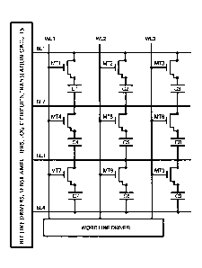
FIG.5 Is a diagram showing multiple bidirectional interconnected memory cells
which may be
considered a functional block diagram and is the preferred circuit
configuration.
FIG.6 Is a diagram 6 is an embodiment of the device utilizing separate
additional bit lines for
bidirectional memory cells.
FIG.7 Is a diagram of an exemplified embodiment of the device wherein the
operation of
bidirectional memory is designed utilizing a combination of two transistors
and one capacitor per
memory cell.
FIG.8 Is a diagram an embodiment of the device utilizing separate bit lines
for bidirectional memory
.. cells.
F1G.9 Is a diagram configured as an exemplary embodiment for the device for
EEPROM "read only
memory" applications
FIG.10 Is a diagram of an exemplary embodiment of the logic circuitry required
for the READ
operation of bidirectional memory.
FIG.11 Is a diagram of a preferred embodiment of the logic circuitry required
for the READ
operation of bidirectional memory.
F1G.12 Is a diagram of a voltage schematic showing the voltage reference of
dual sense amplifiers.
FIG.13 Is a diagram showing a circuit of the device in which the information
can be stored on or
translated from a negative reverse bias voltage.
CA 3030723 2019-01-21
23
FIG.14 Is a diagram representing four possible configurations of the definable
translation
circuits ability to affect the READ state of bidirectional memory cell(s).
FIG.15 Is a diagram where the negative reverse bias voltage stored on a
bidirectional memory
cell, represents the information as being in a 0 and 1 state simultaneously,
also referred to as
superposition.
FIG.16 Is a diagram representing possible configurations of the definable
translation circuits
ability to affect the state bidirectional memory cell(s) in a state of
superposition.
15
25
Date Recue/Date Received 2024-03-11
24
Detailed description
Figure 1 is a diagram showing a single cell of a preferred circuit
configuration for the improved
bidirectional DRAM (dynamic random-access memory). The operation of the memory
cell requires
initially charging a capacitor Cl to store information, this is accomplished
through a similar
operation to traditional DRAM memory cells (not shown). The charging operation
of the capacitor
Cl can be accomplished in one of two polarizations, positive or negative, with
the use of a memory
transistor MT1, bit lines 1 and 2 BL1, BL2. Where bit lines 1 and 2 BL1, BL2
individual voltage
states are dependent upon the desired charging bias of Cl, and with use of
word line 1 WL1, and
.. with the adjacent pluralities of bidirectional memory cells (not shown)
utilizing additional word lines
for example word line 2 WL2.
The operation of the preferred embodiment allows for a similar framework to
existing DRAM and
SRAM (static random-access memory) memory systems, though with a
differentiated circuit
topology. Specifically, operational and circuit layout similarities include,
as a general non-limiting
comparison to circuits and their operation, organizational address layouts,
bit line driver(s) general
operational principles and capabilities, word line driver(s) operation, sense
amplifier(s) (latches)
general operation, the general interconnection with subsequent systems and
processors, for
example the central processing unit CPU. This includes similarities to
individual cell address
identification layout styles, charging (WRITING), READING (paging) and then
maintaining regular
recharging called REFRESHING in order to ensure and maintain the stored
information, with the
addition of an additional bit line BL2 for operation when compared to
traditional DRAM. The
additional bit line BL2 is utilized to allow the alternation of voltage
potentials between bit lines BL1,
BL2, in a bidirectional memory system, and reverse bias charging (WRITE
operations) of capacitor
Cl. Wherein instead of a ground line (not shown) in traditional DRAM memory
cells, a negative
.. polarization may be applied to the capacitor Cl by charging bit line 2 BL2
with a higher voltage
potential then bit line 1, where bit line 1 serves as the lower voltage
potential or ground allowing
charging current to flow through the capacitor Cl in a reverse bias. This
reverse bias may also be
used for subsequent REFRESH operations, and may additionally be used for READ
operations,
though bit line 2 BL2 may not be required for some additional embodiments for
READ operations.
The operation of the bidirectional memory in figure 1 is the preferred
embodiment of a single cell
and organizational implementation utilizing a single transistor MT1, and
figure 2 is an exemplary
embodiment utilizing two transistors MT1, MT2 both with similar operation. The
operation in this
embodiment is carried out by first connecting bit line 1 BL1 to a positive
voltage supply, and bit line
CA 3030723 2019-01-21
25
2 BL2 to a negative or lower voltage supply or state. Then by turning on
transistor MT1 by turning
on word line 1 WL1 as shown in figure 1, or by turning on transistors Mil/ MT2
by turning on word
line 1 WL1, as shown in figure 2, you can charge the capacitor Cl in a forward
positive bias. Or by
alternating the positive voltage supply to bit line 2 BL2 and the negative or
lower voltage supply to
bit line 1 BL1 you can charge the capacitor Cl in a reverse or negative bias.
Operation may also
include a no charge state by either not charging the capacitor Cl or removing
the charge through a
WRITE action with no charge present, or reverse/ inverse charge present on bit
lines 1 and or 2
BL1/ BL2.
There are multiple different methods, and separate embodiments, for reading
the information stored
on the capacitor Cl, some non-limiting examples will be discussed, and in
greater detail in further
figure descriptions.
The design of the bidirectional memory in this embodiment is also beneficial
in that when designing
larger arrays (discussed in greater detail in subsequent figures), the circuit
design allows for simple
straight forward design architecture. This is accomplished because the READ
and WRITE
operations are operated by alternating bit line 1 BL1 as the positive voltage
supply, and bit line 2
BL2 as the negative or lower potential voltage, where additional embodiments
may regularly
alternate the bit line configuration and or polarization. This allows, through
activating a single word
line WL1, the WRITE operation of the capacitor Cl in either a forward positive
polarity or reverse
negative polarity. This allows a very straight forward operation with the main
change to typical
DRAM being the required additional bit line BL2, as well as memory address
designations taking
into consideration the additional reverse charging ability of each capacitor
Cl and therefore
additional address designation. By ensuring that address designations take
into account the
secondary charge state, a memory array (not shown) can be operated to exploit
the benefits of
bidirectional memory, which will be discussed in greater depth and detail in
subsequent figures.
Additionally, multiple transistors may be used to perform the operation of
bidirectional memory, a
few nonlimiting examples are referenced herein figure 3 and figure 4. Where in
figure 3 and figure
4, the use of four transistors MT1, MT2, MT3, MT4, as well as figure 3 the use
of two-bit lines bit
line 1 BL1 bit line 2 BL2, as well as word line 1 WL1 and word line 2 WL2.
Where in figure 3 by
utilizing either word line 1 WL2 or word line 2 WL2, you can alternate the
charging of capacitor Cl
where bit line 1 BL1 can remain as the positive, or higher voltage potential,
and bit line 2 BL2 may
remain as the lower voltage potential or ground, and where the alternation of
bit line 1 BL1 and bit
line 2's BL2 voltage potential in this embodiment may not be required. Though
in some
embodiment's dependent upon the design and size of a memory array, alternation
of the voltage
CA 3030723 2019-01-21
26
potentials between bit line 1 BL1 and bit line 2 BL2 may be beneficial and are
therefore referenced
herein.
Additionally, in figure 4 transistors MT1, MT2, MT3, MT4, may be driven
directly from a drive
directory, ledger, virtual memory system, or central processing unit, memory
management unit, and
or additional drive system. And where bit line 1 BL1 and bit line 2 BL2 maybe
utilized to operate,
and or to alternate, their polarizations during WRITE, READ, and or REFRESH
operations.
In traditional DRAM memory configurations (not shown) the capacitor (not
shown) has been used
entirely as an information storage medium, through charge accumulation and
storage. The energy
stored on the said capacitor, controlled by a switch (not shown), has not be
available to be utilized
throughout the device, nor used to power systems in addition to its primary
purpose of information
storage. This said capacitor is also an energy storage asset, and in the
disclosed system and
method may operate as a duality for information and energy storage.
Additionally, the process of charging and refreshing DRAM is incredibly
wasteful. Operated as a
typical RC circuit where the voltage supplied to the memory is regulated and
reduced in order to
reduce losses. This charging process itself wastes 50% of the supplied energy,
and the other 50%
is used only for information storage, then generally discharged to ground and
not utilized further.
Due to the nature of information processing, and the need for high speed
information storage and
refreshing, alternate more efficient systems for charging the said capacitor
such as switch-mode
power supplies are not practical. The integration of this type of charging
system would not be
practical because the charging time required for improving the storage
efficiency of the said
capacitor would interfere with the high-speed operation of storing information
on the said capacitor
memory system, and therefore slow down the operation of the device(s).
This has led to the design and operation of these type of memory systems to
focus on efficiency
through lowering operational voltage, as well as making the capacitance,
storage ability of the
capacitor, low in order not to waste energy while charging, and while
refreshing.
Depending on the particular application the operation can be controlled by the
management system
(not shown) to control charging the storage device(s), bidirectional memory
cell(s) Cl in the circuit
for predictable, or specific actions, and or to specific charge states/
voltage(s). This may include
multiple combinations of said capacitors Cl simultaneously, or sequentially in
real time. This may
include user interactions in live time, and or predetermined states.
In some embodiments as referenced herein a consistent continuous operation
controlled directly
from the management system (not shown) could provide the instruction for READ
and or WRITE
operations for the storage device(s) Cl, to precisely meet the operational
requirements and
CA 3030723 2019-01-21
27
information states designated and may included a predetermined voltage range
for a specific
application, for instance memory writing and subsequent refreshing.
Additionally, this operation and configuration may be used in some embodiments
to operate
pluralities of bidirectional memory cells (capacitors) Cl, and or
bidirectional memory array(s).
Wherein for instance one embodiment could utilize the management system (not
shown) in an
electronic device such as a smart phone, computer, tablet, wearables, servers,
converters,
inverters, computers, processors, electronic devices, that may consist of
billions of individual or
interconnected bidirectional memory cells.
The operation of a computational devices requires large amounts of memory in
order to compute
actions and functions of the device. By utilizing this system and method
memory charging and
discharging can be accomplished while simultaneously being utilized as an
energy source, in
addition to information storage, thereby reducing the energy cost while in
operation. In this
embodiment a management system (not shown) could be used to control a high
plurality of
bidirectional memory cells capacitor(s) Cl, and charging systems (not shown)
or "deflection
converters" (not shown) that operate independently or conjunctly, wherein
frequency, capacity,
voltage operational range, current, and additional determinants may
significantly vary between
each system, which could utilize different points in time of a singular, or
plurality of capacitor(s) Cl
multiple bidirectional memory cells during operation.
In the case of electronics such as smart phones utilizing the disclosed system
and method a
significant reduction of power consumption, and memory component sizing can be
gained, this
includes a larger amount of information storage and improved computing
ability. This is because
capacitors Cl (memory cells) and additional applications of capacitors are use
extensively
throughout the device, for instance large memory arrays and numerous other
operations and
systems. Many of these systems utilize very inefficient RC (resistor-
capacitor) circuits, where the
disclosed system and method could greatly reduce wasted energy in these
devices, and due to the
additional information storage properties of bidirectional memory cells, a
greater amount of
information may be stored, and or the size of memory arrays may be reduced
thereby reducing
cost.
The system and method may utilize a plurality of memory cells, which may
include an extremely
high number of pluralities. For instance, in the case of a memory bank, a
device may contain
billions of transistors MT1 as an example, controlling billions of capacitors
Cl as an example, for
operations including charging, discharging, writing, reading and or refreshing
commands,
executable across numerous systems.
CA 3030723 2019-01-21
28
In many embodiments of the disclosed system and method this inclusion of
charging systems, such
as deflection conversion, would be greatly beneficial and are referenced as
possible embodiments.
Figure 3 and 4 are diagrams of embodiments of the device, bidirectional
memory, utilized for
electronic memory systems. These diagrams and designs of the device is to
allow for a bidirectional
charging, refreshing, retrieving, and information processing.
These circuit designs allow for the selection of four separate transistors for
combinations in this
example non-limiting examples MT1, MT3 which for this operation are WRITING
(charging) the
capacitor Cl in a positive bias, this bias includes for charging, refreshing,
and or retrieving the
information from the capacitor Cl. This bias is because bit line 1 BL1 in this
embodiment is
connected to a positive voltage supply and bit line 2 BL2 is connected to a
negative voltage supply,
for this non-limiting example.
When selecting transistors MT2, MT4 which for a charging operation, a WRITE
operation, are thus
in a negative bias, for charging, refreshing, and or retrieving the
information from the capacitor Cl.
This bias is because in this reverse orientation bit line 1 BL1 is connected
to a negative voltage
supply and bit line 2 BL2 is connected to a positive voltage supply and or
voltage differential, used
in this non-limiting example. Which could in additional embodiments utilize
different combinational
arrangements of these components, and or bit lines polarizations, to charge
the capacitor Cl, and
or operate inversely to the described operational arrangement example. This
may additionally
include and or require bit lines 1 and 2 BL1, BL2 to regularly change
orientation, and or operate as
READ lines, that may also include the pre-charging of the bit lines BL1, BL2
before and or during a
READ operation.
The device in any of the disclosed figures may be connected and controlled by
any number of
management systems (not shown) and techniques and may include a system
controller(s) (not
shown) and or microcontroller (not shown) and or central processing unit "CPU"
(not shown). The
device may be controlled manually, automatically, by a computer code or
script, embedded system,
or artificial intelligence, controlling commands of the device, connected to
the circuit, and may use a
plurality and multitude of different switching devices and or transistors in
additional to or from MT1,
MT2, MT3, MT4, and may include an interface(s), current and polarity control
devices, and may
comprise different switching device and or capacitor C1 / electrostatic
storage device
arrangements. Wherein one preferred embodiment is in an improved dynamic
random-access
memory (DRAM) configuration, configured to allow the integration and
beneficial operation of the
CA 3030723 2019-01-21
29
device into computers, information processors, and electric devices. The
circuit may utilize power
available from a singular circuit or operate on a separate isolated power
source(s) (not shown).
The input and output of each electrostatic storage device Cl and may be
connected to separate
output switches MT1, MT2, MT3, MT4 or a single switch, and or relay(s) (not
shown) or not, and or
transistor(s) MT1, MT2, MT3, MT4 or not, and may include multiple relay poles
which could be any
number of different types or styles for electronically controlled switching
and or current control
device(s), with all or some switches controlled by a CPU (not shown) or paired
with an existing
CPU (not shown), in a non-limiting example of an embedded, and or plug in
system, and or slave
system, device and or circuit.
The CPU (not shown) may be controlled by a management system (not shown),
computer code or
script, embedded system, or artificial intelligence, that tells the system
controller (not shown), to
send a signal to relay's (not shown) and or transistors MT1, MT2, MT3, MT4,
and or switches,
which may be connected to a power control device and or management system (not
shown).
The device may be connected to a power converter circuit, and or system (not
shown), charge
booster/ converter, and or multiplier and or buck converter, and or flyback
converter, and or
resonance converter, and or switch mode power supply, and or control circuit,
which may or may
not provide current to a load (not shown), and or another storage device (not
shown) to create
usable work, instead of directly grounding which is the typical operation of
DRAM memory circuits.
In an additional embodiment the current after the converter (not shown) is
looped back into the
circuit, to create a feed back circuit and system, which may be connected
after the converter circuit
(not shown), and which may be connected into the power supply side of the
storage device Cl that
is gaining a charge, and may be converted to a higher voltage state to ensure
current draw. The
capacitor Cl may be connected in either a positive polarity, and or negative
polarity configuration,
this may also include additional pluralities of storage devices Cl, power
converters, and or inverters
or both (not shown), and or current control devices (not shown).
In some embodiments a positive feedback into the positive power line before
the capacitor Cl
being charged, and is an exemplified embodiment, which may require a
converter, where the
voltage state of the converter (not shown) at, and or above, the power line
voltage to ensure a
continuous current draw.
Additionally some embodiments the device may utilize a management system (not
shown) as a
component of the device, which may control various functions, some of which
may consist of one or
more of the following non-limiting examples; the operation of all or some of
the electronically
operated components, the charging and or connecting and or disconnecting of
individual or
CA 3030723 2019-01-21
30
combinational arrangements of an electrostatic storage device(s) Cl, with
transistors MT1, MT2,
MT3, MT4. This may include storage device contact, contact point(s), and or
connection, power
regulation means for regulating power; a memory section, a search starting
means for starting a
search; measurement data acquiring means, for acquiring magnetic field data
and or electric power
data, the magnetic field data being measured values of the energy sources and
or magnetic field,
and or capacitor/ electrostatic storage device Cl data, and or bidirectional
memory cell data,
including but limited to; current charge state, polarization, bias, voltage
level, address, location,
orientation, refresh sequence and or rate.
The electric power data representing information associated with electric
power that is outputted
from the energy source, and or on or after the electrostatic storage device
Cl, and or storage
device(s) Cl memory cells, structures, and or lattices. The power converter(s)
(not shown) required
operation, used by a management system (not shown), and or used to store
energy on the
electrostatic storage device Cl, and or different circuit power lines, and or
sources.
Functions may also include deriving means for deriving a relational equation
that holds between the
magnetic field data and electric power data to maintain target values
including voltage and current
output, and or bidirectional memory storage device Cl voltage potential state,
and or feedback
voltage state. Monitoring functions for abnormal state determining and may
include means for
determining whether or not an energy source, a storage device Cl, or any
switching device(s) MT1,
MT2, MT3, MT4, energy transforming and or converting (not shown), and or
managed circuits are
in an abnormal state.
Searching functions, and a search procedure, selecting means for selecting,
and in accordance
with a result of determination. An abnormal state determining means, a
procedure for managing
abnormal energy source(s), magnetic field(s), accumulation devise(s),
capacitor(s) and or
bidirectional memory cell(s) Cl and or storage device(s), switching devise(s)
MT1, MT2, MT3, MT4,
management circuit(s), converter(s) and or inverter(s) (not shown).
In some embodiments, a management system (not shown) is needed to facilitate
managing an
electric current, then switching one or a combination of transistors MT1, MT2,
MT3, MT4, and an
electrostatic storage device and or bidirectional memory cell(s) Cl into a
current stream, and or
connecting power. Then storing the collected charges in an electrostatic
storage device and or
bidirectional memory cell(s) Cl, while simultaneously converting and
regulating output power, and
or feeding the current back into the power supply, to flow into the
electrostatic storage device and
or bidirectional memory cell(s) Cl, then switching collection device(s) Cl in
circuit orientation,
changing its current task and or operational state, and or disconnecting it
from the circuit, with a
switch, and or switches MT1, MT2, MT3, MT4. Then the storage device and or
bidirectional
CA 3030723 2019-01-21
31
memory cell(s) Cl may and or may not discharge collected charges, which may be
a full, or partial
discharge, it may additionally operate as a typical DRAM memory cell wherein
operation requires
periodic refreshing, wherein the information is stored and made available to
the processor.
A current and or voltage measuring/ holding devise(s) (not shown) may be used
as part of the
circuit, including non-limiting examples of operational amplifiers,
comparators, latches (sense
amplifiers), buffers, registers, decoders, coders, cash memory and or memory
bus, switches MT1,
MT2, MT3, MT4, accumulators and or electrical storage device(s), and or
including the preferred
capacitors and or bidirectional memory cell(s) Cl. Some embodiments may
utilize circuit controllers
(not shown) for instance a non-limiting example utilizing pulse width
modulation "PWM". In some
embodiments a simplified management system (not shown) may be beneficial. In
some
embodiments utilizing no management system instead using current oscillators
an or timers (not
shown), clock(ing), comparators (not shown), op amps (not shown), decade
counter (not shown), to
control the switch(ing) of transistors MT1, MT2, MT3, MT4, and capacitor Cl.
A management system (not shown) is preferred in the majority of embodiments to
ensure optimal
.. system performance, accuracy, bidirectional memory operation, and
efficiency. In order for
information to be communicated and interpreted for command allocation, memory
address
designation, storage, recall (paging) and information processing, including
operational
characteristics, and predetermined target value ranges. This also includes
output characteristics,
discharge relational information including combinational arrangement output
power data, cluster
and module combination data, looping circuit and or feedback value, and duty
cycle optimization
equations.
The management system (not shown) may also incorporate a learning effect, or
artificial
intelligence, interpretations can be interpreted by the central processing
unit CPU (not shown),
which can send instructions to the system controller (not shown), which can
then send command
signals to active switching transistors MT1, MT2, MT3, MT4, and control
systems, and components,
to control predetermined, or instructed operational target values of storage
device(s) and or
bidirectional memory cell(s) Cl, recharging/ refreshing characteristics,
output characteristics,
feedback characteristics, converter duty cycle/ switching frequency, memory
selection and or
operation, word line selection and or operation, bit line selection and or
operation circuit selection
and or operation, system operations including various subsystems, and
device(s) functions.
Figure 5 is a diagram showing multiple bidirectional interconnected memory
cells which may be
considered a functional block diagram, where the circuits and components may
be considered
CA 3030723 2019-01-21
32
blocks of a system, for their general function, or for a device that may be
used to confer the
action of their specific block, as such blocks may be omitted, combined, or
substituted within an
operable configuration of the device to facilitate the operation within the
scope of the disclosure,
where diagram 5 is configured as the preferred circuit arrangement and
embodiment. In this
embodiment the use of multiple bidirectional interconnected memory cells
allows the operation
of capacitors Cl, C2, C3, C4, C5, C6, C7, C8, C9 utilizing transistors MT1,
MT2, MT3, MT4,
MT5, MT6, MT7, MT8, MT9, creating an interconnected matrix, additionally
operable with word
lines WL1, WL2, WL3, and bit lines BL1, BL2, BL3, BL4.
In this non-limiting preferred example, the layout of the circuit is designed
as a memory DRAM
address schematic, operated as a plurality of interconnected memory cells,
though operated
independently, in an interconnected framework. This allows the operational
characteristics to be
precisely tailored to meet the requirements specific to each independent
system. This is
especially beneficial where voltages may operate at different potentials,
meaning that the
required operational voltage may vary, or be at a different state(s) then each
separate
independent system and or memory array. For instance, the bidirectional DRAM
may operate at
2 volts when charging individual memory cells, and additionally for charging
multiple memory
cells, and or capacitors Cl, C2, C3, C4, C5, C6, C7, C8, C9 simultaneously.
When charging
bidirectional memory cells in a series arrangement may require increasing this
operational
charging (WRITING) voltage, to for instance 6 volts if charging any three of
said capacitors
simultaneously, so each of said capacitors retains a 2-volt charge, where
certain embodiments
may require balancing circuitry when charging multiple capacitors and/or
bidirectional memory
cells simultaneously.
This operation of being able to charge multiple capacitors, for instance
groupings of any of the
capacitors Cl, C2, C3, C4, C5, C6, C7, C8, C9 in a single operation, with the
use of different
transistor combinations selected from MT1, MT2, MT3, MT4, MT5, MT6, MT7, MT8,
MT9, or
plurality, in this embodiment by turning on any specific combination of said
transistors is very
beneficial, in that by utilizing this operation the speed of processing may be
increased due to
the fact multiple WRITE operations can be accomplished with a single WRITE
operation,
reducing refresh time allocation and therefore latency.
For instance, during the regular operation of a device the processor may allow
for the processing of
7 bytes of information, utilizing a 64-bit processor, with 1 byte of reserved
for command allocation.
This means that 56 bits can be processed per cycle, though operated at a very
high clock frequency
for instance in the gigahertz, with current clock speed being limited at
around 5 GHz. In this
operation the physical memory may be used and combined with virtual memory to
more fully exploit
the memory system, so for the purpose of this operation the CPU doesn't
necessarily
Date Recue/Date Received 2024-03-11
33
recognize multiple physical addresses, instead it recognizes a single physical
memory address(es)
or plurality, though this may consist of any plurality of bidirectional memory
cells in series.
This layer of obscurity allows, with the use of disclosed system and method of
bidirectional
memory, the ability to exploit virtual memory (as a non-limiting example) to
encode multiple
interconnected memory cells simultaneously. Where in the example of a
processor processing 56
bits, for processing and specifying multiple addresses, and then WRITING or
READING individual
cells. Wherein if virtual addresses were designed to reflect any combination
of the multiple
interconnected capacitors Cl, C2, C3, C4, C5, C6, Cl, C8, C9, and or any
plurality in a memory
array, by specifying specific transistors from MT1, MT2, MT3, MT4, MT5, MT6,
MT7, MT8, MT9, or
any plurality in a memory array, to allow this in series charging
configuration and adequate voltage
was supplied, you could charge a group of capacitors Cl, C2, C3, C4, C5, C6,
C7, C8, C9 or
plurality with a single write and or refresh action. Where this group of
capacitors could later be
accessed individually for READ operations, therefore preforming more actions
over a defined
period of time and speed up processing, which could additionally be exploited
during allocated
refresh operations.
This could be used in additional embodiments to increase the transfer and
dissemination of
information, where for instance information is shared between to computers
(not shown). The first
computer (not shown) provides an information set that includes a memory
WRITING program. This
program includes instructions to WRITE into memory the desired information
utilizing in series
sequential capacitors Cl, C2, C3, C4, C5, C6, C7, C8, C9 or plurality,
charging in the bidirectional
memory framework, allowing the information to be stored into memory at
expedited rates. Then as
the processor READS the information from physical and or virtual addresses, it
is unaware that
multiple bits had been WRITTEN simultaneously to memory by means of an
interconnected
architecture. This operation could be used to WRITE a few sequential
capacitors Cl, C2, C3, C4,
C5, C6, C7, C8, C9, or multiple plurality, with a single two transistor
arrangement MT1, MT2, MT3,
MT4, MT5, MT6, MT7, MT8, MT9 or plurality, utilizing in series and or cross
coupled addresses.
The application and operation of many independently operating, interconnected
bidirectional
memory systems, and circuits, within a device(s) referenced as an exemplified
3-dimensional
construction configuration, and or planar stacked construction which is the
preferred embodiment of
this disclosure. This method of integration and operation allows bidirectional
memory technology to
be utilized by many of the systems and operating circuits electronic devices
contain. The ability to
offer improved information storage to a device and by not negatively impacting
the devices
operation, is practically implementable, and very beneficial. Additionally,
connected to word lines
WL1, WL2, WL3 is a word line driver and/or driver circuit including line and
column selectors, block
CA 3030723 2019-01-21
34
selectors. And connected to bit lines BL1, BL2, BL3, BL4, includes different
circuits including
bit line driver's that allow the alternation of bit line polarities and
voltage potentials, sense
amplifiers, differentiators, logic circuits, translation circuits, definable
translation circuits,
constrained translation circuits, subsequent combinational definable
translation circuits, and
general processor and computer circuitry including line and column selectors,
block selectors,
buffers, memory cash, and central processing unit "CPU", where an embodiment
of bidirectional
memory includes an array of bidirectional memory cells that may be Write
accessed to store
data and Read accessed to retrieve the stored data.
For operation of a bidirectional memory array a bidirectional cell is selected
during either a
READ operation, or a WRITE operation, by selecting its bank, row, and column.
The bank, row,
and column that are chosen are determined by a binary code. For a non-limiting
example, an
address may comprise a 16-bit binary code for controlling the WRITE and READ
operations.
More particularly, the 16-bit binary may comprise two separate 8-bit binary
codes one for
selecting the row and the other for the column, which may further be coupled
to a row decoder
and a column decoder and host bus. In response to each 8-bit code, the row
decoder may
generate 2 outputs, which allows up to 256 different address patterns. As
well, the column
decoder may generate another 2 outputs, which allows a combined matrix of
selectable memory
cells from 256 rows and 256 columns.
Bidirectional memory cell addresses may be defined or assigned through a
number of possible
schemes, one possible nonlimiting example, that maintains the structure and
consistency
existing DRAM memory structures, is by sequentially identifying the memory
cells both for the
positive and negative charge state's as adjacent, and or individual addresses,
and/or a
sequential memory cell address identification scheme and configuration.
Another nonlimiting
example may include designating the memory cells within their traditional
address framework,
where identifying the negative charge on a bidirectional memory cell is
designated as an inverse
or negative address (-), therefore allowing exact address specification with
existing addressed
designation frameworks, and referencing the cell polarity by means of a
polarity symbol which is
the preferred embodiment of address designation as this may allow a simple
straight forward
operation to utilize a row and column decoder, while maintaining existing code
addressable
architectures. Though many possible address schemes are possible and do not
depart from the
scope of the disclosed method.
This circuit lays out the basic design of a memory system and or array
consisting of nine
interconnected cells, which may additionally be constructed 3-dimensionally or
in some
Date Recue/Date Received 2024-03-11
35
embodiments a planar construction with each interconnected array comprising
one or part of a
plane, and additionally interconnected arrays being stacked, or layered
sequentially, and with each
array comprising any number of interconnected cells with any plurality of
layers or stacks or arrays.
Additionally as with previous prior art schemes for DRAM the operation of
reading the bidirectional
memory cell is destructive and during a READ operation the capacitor may, and
generally will,
require a recharging operation, for simplicity this circuit arrangement has
been omitted from the
figures, with the reference that this operation in the disclosed system and
method is accomplished
with two bit lines, a non-limiting example being, bit line 1 BL1 and bit line
2 BL2, where polarization
of each bit line BL1, BL2 is dependent upon the bias of the capacitor Cl
recharging operation, as
well as a word line a nonlimiting example being word line 1 WL1, activating a
transistor and
capacitor for instance a non-limiting example of transistor MT1 and capacitor
Cl .
Figure 6 is an embodiment of the device utilizing separate additional bit
lines BL1, BL2, BL3, BL4,
BL5, BL6, for bidirectional memory cells. Separate bit lines may be very
beneficial in certain
embodiments where parasitic capacitances may interfere with the operation of
multiple bidirectional
memory cells (capacitors) Cl, C2, C3, C4, C6, C6, C7, C8, C9, or plurality,
operating in parallel or
sequentially wherein the use of separate bit lines between cells allows
independence of the
memory array's individual cells. Where for instance multiple processors are
accessing memory cell
information simultaneously, and where utilizing joint lines as referenced in
figure 5 conflicts may
occur, for instance utilizing combinations of transistors MT1, MT2, MT3, MT4,
MT5, MT6, MT7,
MT8, 11/1T9, or plurality, for charging memory cells with inverse
polarizations along the same bit
lines, where this may cause the inability to operate specific verticals or
horizontal memory rows or
columns simultaneously, depending on the physical memory address accessed with
word lines
WL1, WL2, WL3. Therefore, in certain embodiments the segregation of individual
bidirectional
memory cells by incorporating additional bit lines BL4, BL5, BL6, or
plurality, may be preferred.
It should also be noted that many embodiments may utilize a drive directory or
directory, and may
exist as virtual directories, meaning the specific directory is a ledger, and
not a physical separate
circuit, or system. This could be very advantageous for ease of use and
operation if the ledger
operates comparably to a virtual memory system, in that information is
recorded, and stored, for
later reference and use, thereby allowing a program to allocate physical
storage, referenced from
and recorded into a ledger(s), this reference to the operation of a virtual
directory is included as an
example and not meant to limit the scope of possible memory management
operations, and virtual
directories where embodiments and descriptions are for some of a number of
possible
implementations, operational systems and embodiments.
CA 3030723 2019-01-21
36
As well additional embodiments could also include complex READ and WRITE
address designs,
operating multiple transistors, that control multiple charging operations
throughout an individual, or
multiple arrays. This may be very beneficial to encode information at
expedited rates, for instance
writing multiple capacitors across multiple bidirectional memory cells
simultaneously, thereby
preforming a WRITE operation that would normally take many individual
sequences, in a single, or
reduced amount of WRITE operations.
Figure 7 is an exemplified embodiment of the device wherein the operation of
bidirectional memory
is designed utilizing a combination of two transistors and one capacitor per
memory cell operation,
with an interconnected matrix of bidirectional memory cells. In this
embodiment the use of two
transistors per memory cell MT1, MT2, MT3, MT4, MT5, MT6, MT7, MT8, MT9, MT10,
MT11,
MT12, MT13, MT14, MT15, MT16, MT17, MT18, or plurality, is to allow a more
complex charging
(WRITE) operation of multiple bidirectional memory cells, capacitors Cl, C2,
C3, C4, C5, C6, C7,
C8, C9, or plurality. This circuit design in certain embodiments may use
transistors MT2, MT4,
MT6, MT8, MT10, MT12, MT14, MT16, MT18, or a plurality of transistors as pull
up transistors, and
transistors MT1, MT3, MT5, MT7, MT9, MT11, MT13, MT15, MT17, or a plurality or
plurality of
transistors as pull down transistors, though said sets of transistors may be
alternated or dual
directional in additional embodiments, where they may be utilized to allow
cross charging of
capacitors in both series and parallel combinations. This is accomplished by
defining the voltage
potentials of bit lines BL1, BL2, BL3, BL4, or plurality, and selecting cells
by charging word lines
WL1, WL2, WL3 or plurality. As discussed in figure 5 this may be greatly
beneficial to accomplish
multiple WRITE operations in a single action, as well as allowing a faster
transfer of information by
providing memory write instructions where the process of writing information
to memory requires
less sequential operations.
.. Figure 8 is an embodiment of the device utilizing separate bit lines for
bidirectional memory cells
and is designed utilizing two transistors and one capacitor per memory cell,
and additional separate
bit lines. Separate bit lines may be very beneficial in certain embodiments
where parasitic
capacitances may interfere with the operation of multiple bidirectional memory
cells operating in
parallel or sequentially wherein the use of separate bit lines between cells
allows independence of
the memory array's individual cells. Where for instance multiple processors
are accessing memory
cell information simultaneously, In this embodiment the use of two transistors
per memory cell MT1,
MT2, MT3, MT4, MT5, MT6, MT7, MT8, MT9, MT10, MT11, M112, M113, M114, MT15,
MT16,
MT17, MT18, or plurality, is to allow a more complex charging (WRITE)
operation of multiple
bidirectional memory cells, capacitors Cl, C2, C3, C4, C5, C6, C7, C8, C9, or
plurality. This circuit
CA 3030723 2019-01-21
37
design by utilizing transistors MT2, MT4, MT6, MT8, MT10, MT12, MT14, MT16,
MT18, or a
plurality of transistors as pull up transistors, and transistors MT1, MT3,
MT5, MT7, MT9, MT11,
MT13, MT15, MT17, or a plurality or plurality of transistors as pull down
transistors, though said
sets of transistors may be alternated or dual directional in additional
embodiments, where they may
be utilized to allow cross charging of capacitors in both series and parallel
combinations by
controlling specific current paths and limiting conduction across any specific
or plurality of said
capacitors, or plurality. This is accomplished by defining the voltage
potentials of bit lines BL1,
BL2, BL3, BL4, BL5, BL6, or plurality, and selecting cells by charging word
lines WL1, WL2, WL3
or plurality. As discussed in figure 5 this may be greatly beneficial to
accomplish multiple WRITE
operations in a single action, as well as allowing a faster transfer of
information by providing
memory write instructions where the process of writing information to memory
requires less
sequential operations.
One method for a READ operation includes pre-charging both bit lines to a
specific and or equal
voltage, then by turning on different arrangements of transistors MT1, MT2,
MT3, MT4, MT5, MT6,
MT7, MT8, MT9, MT10, MT11, MT12, MT13, MT14, MT15, MT16, MT17, MT18, which may
include
single or multiple of said transistors simultaneously, and may require an
inverse voltage polarity
applied to the word line WL1, WL2, WL3, you can determine the charge state of
a capacitor Cl,
C2, C3, C4, CS, C6, C7, C8, C9, if there is an increased or decreased voltage
on a set of the bit
lines BL1, BL2, BL3, BL4, BL5, BL6. Additionally, this may be accomplished by
activating any
individual transistor MT1, MT2, MT3, MT4, MT5, MT6, MT7, MT8, MT9, which may
require an
inverse charge applied to word lines WL1, WL2, WL3, and comparing the charge
READ from a
capacitor Cl, C2, C3, C4, C5, C6, C7, C8, C9, against a reference voltage,
wherein this individual
reading operations could be preformed sequentially with all or some of the
transistors MT1, MT2,
MT3, MT4, MT5, MT6, MT7, MT8, MT9, MT10, MT11, MT12, MT13, MT14, MT15, MT16,
MT17,
MT18, to determine charge state and polarity.
The design of the bidirectional memory described in this preferred embodiment
is also beneficial in
that when designing larger arrays (discussed in greater detail in subsequent
figures), the circuit
design allows for simple straight forward design architecture. This allows,
through activating a
single word line WL1, WL2, WL3, and set of bit lines BL1, BL2, BL3, BL4, BL5,
BL6 the WRITE
operation of the capacitor(s) Cl, C2, C3, C4, C5, C6, C7, C8, C9, in either a
forward positive
polarity, or reverse negative polarity. This allows a very straight forward
operation that is very
similar to a traditional SRAM WRITE operation, with the main changes being the
required additional
word line (not shown) in vertical plain operations, as well as address
designations taking into
consideration the additional reverse charging ability of each capacitor C1,
C2, C3, C4, C5, C6, C7,
CA 3030723 2019-01-21
38
C8, C9. By ensuring that address designations take into account the secondary
charge state as
well as word line address designation, the memory array can be operated to
exploit the benefits
of bidirectional memory which will be discussed further in subsequent figures.
Figure 9 is a diagram showing multiple bidirectional interconnected memory
cells which may be
considered a functional block diagram, where the circuits and components may
be considered
blocks of a system, for their general function, or for a device that may be
used to confer the
action of their specific block, as such blocks may be omitted, combined, or
substituted within an
operable configuration of the device to facilitate the operation within the
scope of the disclosure,
where diagram 9 is configured as an exemplary embodiment for the device for
EEPROM "read
.. only memory" applications. In this embodiment the use of multiple
bidirectional interconnected
memory cells allows operation by means of transistors MT1, MT2, MT3, MT4, MT5,
MT6, MT7,
MT8, MT9, MT10, MT11, MT12, MT13, MT14, MT15, MT16, MT17, MT18, creating an
interconnected matrix, additionally operable with word lines WL1, WL2, WL3,
WL4, WL5, WL6,
WL7, WL8, WL9, and bit lines BL1, BL2, BL3, BL4.
It should be noted the operation of the device may operate and or be
constructed as either a
rewritable ROM or non-rewritable ROM and may include a number of typical ROM
types
including Mask ROM, Programmable ROMs (PROMS), Erasable Programable ROMs
(EPROM), Electrically Erasable Programmable ROMs (EEPROM), Electrically
Alterable
Programmable ROMs (EAPROM), Flash Electrically Erasable Programmable ROM's
memory
(EEPROM), as a few non-limiting examples and are referenced herein as possible
embodiments.
In this layout design the initial charge process may be accomplished a number
of ways, in this
non-limiting example a bit line BL1, BL2, BL3, BL4, is activated with a
specific voltage and a
word line WL1, WL2, WL3, WL4, WL5, WL6, WL7, WL8, WL9, is activated with
specific
voltage. The charging word lines WL2, WL3, WL5, WL6, WL8, WL9, generally have
a higher
voltage to permanently, or non-permanently encode the device to a fixed on of
off state. This
allows the operation of determining the information stored within a
bidirectional memory cell,
which in this non- limiting example is comprised of two transistors.
Each transistor is connected to one-bit line, and two-word lines, and either a
ground
connection and lower potential, or voltage source and higher potential. In
this design by
turning on transistor MT1 by means of word line 1 WL1 and bit line BL1 you can
use the
ground connection of the transistor to pull down the voltage of a bit line BL1
during READ
operations allowing a clearly definable 1st state. As well in this design you
can utilize
transistor MT2 by means of word line 1 WL1 and bit line BL1 connected to a
higher
voltage potential or source to pull up or increase the voltage potential of
the bit line 1 BL1
.. during READ operations allowing a clearly definable 2nd state. Finally, you
can
Date Recue/Date Received 2024-03-11
39
allow for a third clearly identifiable state during READ operations by not
utilizing transistor MT1
or MT2, by not initializing or encoding them, and maintaining the voltage of
the bit line 1 BL1
during read operations by means of word line 1 WL1 and bit line BL1, where in
the preferred
embodiment the voltage potential state on a bit line 1 BL1 during READ
operations is fifty
percent of the voltage potential of transistor MT2's input source.
The operation of this exemplified embodiment of a bidirectional memory cell
requires encoding
the transistor to store information, this is accomplished by utilizing a high
voltage to encode
(WRITE) the specific transistor either MT1 or MT2 or plurality, depending on
intended
polarization or current flow bias. Using WRITE word lines WL2 or WL3 will
encode transistor
MT1 or MT2 depending on intended polarization or current flow bias, where the
rectifying
diode(s) 30 block the higher voltage from encoding other transistors along
word line 1 WL1
(MT1, MT2, MT7, MT8, MT13, MT14). The READ operation is for this specific
bidirectional
memory cell is accomplished utilizing word line 1 WL1 to provide transistors
MT1 and MT2 with
a current to their gate electrode, and where bit line 1 BL1 is charged to a
nominal voltage
between the low voltage potential of transistor MT1 and higher voltage
potential of transistor
MT2, and will cause the bit line BL1 to assume one of three states during the
READ operation.
The first state where bit line 1 BL1 voltages is pulled up representing a
positive bias or polarity,
the second state providing no change to the voltage of the bit line BL1
representing a neutral
polarity or no charge, and finally a third state where the voltage is pulled
down on the bit line
BL1, representing a negative bias or polarization.
The operation of the preferred embodiment allows for a similar framework to
existing ROM
memory systems, though with a differentiated circuit topology. Specifically,
operational and
circuit layout similarities include, as a general non-limiting comparison to
circuits and their
operation, organizational address layouts, bit line driver(s) general
operational principles and
capabilities, word line driver(s) general operational principles and
capabilities, sense amplifier(s)
general operation, the general interconnection with subsequent systems and
buffer, cache,
register, processors, for example the central processing unit CPU. This
includes similarities to
individual cell address identification layout styles, with the addition of an
additional word line to
encode said transistors charge state with charging word lines WL2, WL3, WL5,
WL6, WL8,
WL9, where in this non-limiting example rectifying diode(s) 30 are used to
control the current
while encoding (WRITING) a specific transistor MT1, MT2, MT3, MT4, MT5, MT6,
MT7, MT8,
MT9, MT10, MT11, MT12, MT13, MT14, MT15, MT16, MT17, MT18.
There are multiple different methods, and separate embodiments, for reading
the information
stored on a bidirectional memory cell, some non-limiting examples will be
discussed, and in
greater detail in further figure descriptions.
Date Recue/Date Received 2024-03-11
40
The design of the bidirectional memory in this embodiment is also beneficial
in that when designing
larger arrays (discussed in greater detail in subsequent figures), the circuit
design allows for simple
straight forward design architecture.
This allows a very straight forward operation with the main change to typical
ROM being the
required additional initializing word lines WL2, WL3, WL5, WL6, WL8, WL9, and
diode(s) 30, for
encoding, WRITE operations. As well as each memory address designation taking
into
consideration the additional required bit spaces in the buffer which may also
need to be taken into
account for the cache and register, when a memory cell is READ as being in a
negative polarization
that has been encoded to represent multiple bits of information, and therefore
requires additional
address designations or allocated spaces in a buffer. By ensuring that address
designations take
into account the secondary charge state, a memory array (not shown) can be
operated to exploit
the benefits of a ROM bidirectional memory, which will be discussed in greater
depth and detail in
subsequent figures.
Additionally, bidirectional memory cells may be driven directly from a drive
directory, ledger, virtual
memory system, or central processing unit, memory management unit, and or
additional drive
system.
Depending on the particular application the operation can be controlled by the
management system
(not shown) to control charging the storage device(s), bidirectional memory
cell(s) in the circuit for
predictable, or specific actions, and or to specific charge states/
voltage(s). This may include
multiple combinations of said bidirectional memory cells simultaneously, or
sequentially in real time.
This may include user interactions in live time, and or predetermined states.
In some embodiments as referenced herein a consistent continuous operation
controlled directly
from the management system (not shown) could provide the instruction for READ
and or WRITE
operations for the bidirectional memory cells, to precisely meet the
operational requirements and
information states designated and may included a predetermined arrangement of
specifically
initialized transistors MT1, MT2, MT3, MT4, MT6, MT6, MT7, MT8, MT9, MT10,
MT11, MT12,
MT13, MT14, MT15, MT16, MT17, MT18, or additional plurality, to form a logical
readable code or
script, program, instruction or the like. It should be noted that he operation
of reading the ROM
bidirectional memory cells is non-destructive during a READ operation.
.. Additionally, this operation and configuration may be used in some
embodiments to operate
pluralities of bidirectional memory cells, and or bidirectional memory
array(s). Wherein for instance
one embodiment could utilize the management system (not shown) in an
electronic device such as
a smart phone, computer, tablet, wearables, servers, converters, inverters,
computers, processors,
CA 3030723 2019-01-21
41
electronic devices, that may consist of billions of individuals or arranged
bidirectional memory cells.
In this non-limiting preferred example, the layout of the circuit is designed
as a memory ROM
address schematic, operated as a plurality of interconnected memory cells,
though operated
independently, in an interconnected framework. This allows the operational
characteristics to be
precisely tailored to meet the requirements specific to each independent
system.
The application and operation of many independently operating, interconnected
bidirectional
memory systems, and circuits, within a device(s) referenced as an exemplified
3-dimensional
construction configuration, and or planar stacked construction which is the
preferred embodiment of
this disclosure.
This method of integration and operation allows bidirectional memory
technology to be utilized by
many of the systems and operating circuits electronic devices contain. The
ability to offer improved
information storage to a device and by not negatively impacting the devices
operation, is practically
implementable, and very beneficial.
Additionally, connected to word lines WL1, WL2, WL3, WL4, WL5, WL6, WL7, WL8,
WL9, is a
word line driver and/or driver circuit including line and column selectors,
block selectors that may be
used to control and or initialize transistor MT1, MT2, MT3, MT4, MT5, MT6,
MT7, MT8, MT9, MT10,
MT11, MT12, MT13, MT14, MT15, MT16, MT17, MT18, and therefor bidirectional
memory cells.
And connected to bit lines BL1, BL2, BL3, BL4, includes different circuits
including bit line driver's,
sense amplifiers, differentiators, logic circuits, translation circuits,
definable translation circuits,
constrained translation circuits, subsequent combinational definable
translation circuits, and
general processor and computer circuitry including line and column selectors,
block selectors,
buffers, memory cash, and central processing unit "CPU", where an embodiment
of bidirectional
memory includes an array of bidirectional memory cells that may be WRITE
accessed to store data
and READ accessed to retrieve the stored data.
For operation of a bidirectional memory array a bidirectional cell is selected
during either a READ
operation, or a WRITE operation, by selecting its bank, row, and column. The
bank, row, and
column that are chosen are determined by a binary code. For an non-limiting
example, an address
may comprise a 16-bit binary code for controlling the WRITE and READ
operations. More
particularly, the 16-bit binary may comprise two separate 8-bit binary codes
one for selecting the
row and the other for the column, which may further be coupled to a row
decoder and a column
decoder and host bus. In response to each 8-bit code, the row decoder may
generate 2 outputs,
which allows up to 256 different address patterns. As well, the column decoder
may generate
another 2 outputs, which allows a combined matrix of selectable memory cells
from 256 rows and
256 columns, with may also utilize additional address designations for WRITE
applications and or
CA 3030723 2019-01-21
42
when READ operations where bidirectional memory cells are each encoded with
multiple bits of
information.
Bidirectional memory cell addresses may be defined or assigned through a
number of possible
schemes, one possible nonlimiting example, that maintains the structure and
consistency
existing ROM memory structures, is by sequentially identifying the memory
cells both for the
positive and negative charge state's as adjacent, and or individual addresses,
and/or a
sequential memory cell address identification scheme and configuration.
Another nonlimiting
example may include designating the memory cells within their traditional
address framework,
where identifying the negative charge on a bidirectional memory cell is
designated as an inverse
or negative address (-), therefore allowing exact address specification with
existing addressed
designation frameworks, and referencing the cell polarity by means of a
polarity symbol which is
the preferred embodiment of address designation as this may allow a simple
straight forward
operation to utilize a row and column decoder, while maintaining existing code
addressable
architectures, with the additional of assignment of the additional information
bits into the buffer,
by accounting for each specific additional bit sequence, each additional bit,
held as a negative
charge. Though many possible address schemes are possible and do not depart
from the scope
of the disclosed method.
This circuit lays out the basic design of a memory system and or array
consisting of nine
interconnected cells, which may additionally be constructed 3-dimensionally or
in some
embodiments a planar construction with each interconnected array comprising
one or part of a
plane, and additionally interconnected arrays being stacked, or layered
sequentially, and with
each array comprising any number of interconnected cells with any plurality of
layers or stacks
or arrays. And may additionally comprise additional word lines (not shown) and
or bit lines (not
shown) for both READ and WRITE operations of bidirectional memory cells, and
may
additionally comprise additional transistors (not shown) for each
bidirectional memory cell for
controlling each cell and or for storing information within each cell, without
departing for the
scope and intended results of the disclosed system and method while still
maintain a narrowed
equivalent design and operation process, and are herein referenced as possible
additional
embodiments.
Figure 10 is a diagram of an exemplary embodiment of the logic circuitry
required for the READ
operation of bidirectional memory, which may be considered a functional block
diagram, where the
circuits and components may be considered blocks of a system, for their
general function, or for a
device that may be used to confer the action of their specific block, as such
blocks may be omitted,
Date Recue/Date Received 2024-03-11
43
combined, or substituted within an operable configuration of the device to
facilitate the operation
within the scope of the disclosure, including the circuitry required to
retrieve and interpret the
three different states (tri-state) of bidirectional memory referenced as
forward bias (positive),
reverse bias (negative), and no charge, states. In this embodiment the charge
stored in a
.. negative bias is READ by the logic circuitry as holding multiple bits of
information, in this
embodiment the negative charge is READ and interpreted as representing "011",
though in
additional embodiments any combination of 0('s) and or 1('s) representing
binary logic may be
stored and or READ and or interpreted by the logic circuitry, buffer, cache,
register, and used by a
CPU (not shown), processor(not shown), computer(not shown), or other
electronic system or device.
.. Traditional memory systems utilized in a binary framework, and operation
have not been fully
exploited to utilize a bidirectional memory system for the purpose of storing
multiple bits of
information. In binary systems each memory cell stores either a 1 or 0, a
single bit of
information of a binary digit, and by utilizing the disclosed system and
method a single memory
cell can represent, and therefore store more than a single bit of information.
This is greatly
.. beneficial and should not be confused with a ternary language or operating
system.
The benefit of storing multiple pieces of information, such as an information
sequence allows
another layer of abstraction within a binary framework. The ability to store
more than a single bit
of information allows the development of new innovative processing systems, it
also allows the
reduction in size of physical memory systems, for instance as reference in
figure 9 ROM
memory. This allows a binary code compression, that may be in conjunction to
additional
compression techniques greatly reducing the required amount of physical memory
cells
required for a specific code, sequence, program, and or mathematical sequence.
This operation for specifically designing the logic circuitry may be
accomplished in some
embodiments by manmade design, or computer analysis based on the most
beneficial design,
or logical design based on specific code sequences, and or simulation or
modeling based design,
without departing from the scope and subsequent embodiments of the disclosure
and referenced
herein. Where the use of a specific circuit design, or switch(s), or
transistor(s), for instance a plurality
of specific logic gate sequence(s) may be use for all or part or utilize an
additional plurality, of an
information sequence, code, mathematical sequence, program or communication.
The benefit of utilizing different information sequences that can be stored on
or translated as the
negative polarization in a bidirectional memory framework provides many
benefits. A major
benefit being the compression of information, this compression benefit may be
further exploited
in additional embodiments by analyzing specific sections of code to determine
the most beneficial
sequence to be stored and translated, then designing the logic circuitry for
that specific section of
Date Recue/Date Received 2024-03-11
44
code. This would allow multiple sections of code to store different
information sequences and
therefor required different logic circuitry to decode the stored and or
translated code section,
thereby maximizing the disclosed system and method, which may then utilize a
field programable
gate array and or CPU. Further these separate information sequences and the
subsequent logic
circuitry, could be stored on a ledger or legend, allowing a clear
communication and interpretation
of information by reading and decoding the translated or stored code with the
appropriate logic
circuitry for each information or code sequence or section.
Even ternary systems are not designed to utilize memory for the purpose of
allowing individual
memory cells to hold more than a single bit of information. The beneficial
design of ternary systems
being the natural mathematical operation of balanced ternary systems, or the
reduction of required
bits for information processing due to the ternary language encoding system
and legend. Therefore,
another embodiment is utilizing the disclosed system and method to store more
than a single bit of
information for each memory cell utilized in a ternary operation and or
framework.
Even quantum computers are not designed to utilize memory for the purpose of
allowing individual
memory cells (qubits) to hold more than a single bit of information. The
beneficial design of
quantum computer systems being the quantum features exploited for operation
including; states of
superposition, entanglement, interference, as a few examples. Therefore,
another embodiment is
utilizing the disclosed system and method to store more than a single bit of
information for each
memory cell utilized in a quantum operation and or quantum computer framework.
In one embodiment of the disclosed system and method, that may utilize a
variety of designs, for a
specific logic circuitry design, used to decode the representation of
information stored on a
bidirectional ROM memory cell follows:
The operation of one nonlimiting example of the READ circuitry required to
differentiate and attain
the charge state of a bidirectional memory cell is as follows; During a READ
operation a bit line, in
this case bit line 1 BL1, may be pre-charged, and in this nonlimiting example
is pre-charged to 50%
of the source voltage, though may additionally be at or sub VDD levels. A
sense amplifier 40A
which is non-inverting READS the voltage from bit line 1 BL1 and compares it
against a set
reference voltage (threshold), wherein the reference voltage VRef trip point,
threshold, is a high
state trip point. This allows an output of 1, or ON state, if the voltage READ
from bit line 1 BL1
transverses and saturates the VThresh- VRef point, initiating a state change
from 0, to 1. The ON
output of the sense amplifier 40A is then directed to a D-type flip-flop 65A,
where the sense clock
may initiate a state change allowing a latch to occur, reinforcing the charge
state, the flip-flop's
55A inverting compliment output -(2 which therefore outputs an OFF, or 0 state
which is routed to a
NOT Gate (inverter) 90 that reinverts the state back to an ON state and is
then sent to an OR Gate
CA 3030723 2019-01-21
45
80 for output communication of the voltage state from sense amplifier 40A, and
where the flip-flops
55A non-inverting output Q is routed to AND Gate 70.
Additionally, a sense amplifier 40B is connected to READ the voltage from bit
line 1 BL1 and is
configured to be inverting, where if bit line 1 BL1 has a voltage state
present that crosses below its
VThresh its voltage reference VRef, or low point reference, will initiate an
ON state, or 1, signifying
a negative charge state on the bidirectional memory cell. This ON state is
sent to a D type flip-flop
65B, which outputs the non-inverting output Q in an ON state to AND Gate 70
and inverting
compliment output signal to a NOT Gate 90 (inverter) that inverts the inverted
state back to an
ON state that sends the signal to the memory management unit 230, and a
control transistor 20 or
plurality, that controls a singular or plurality of logic gates 80, 70, 70, or
control components, within
a definable translation circuit, to control and or interpret the output
information state of a negatively
charged bidirectional memory cell.
The control transistor 20 outputs a signal to the memory management unit 230,
allowing the
memory management unit 230 to interpret the negative voltage charge READ from
the bidirectional
memory cell.
In certain embodiments will allow for additional sequential information slots
within the buffer or
register to be assigned. Additionally, other embodiments, specifically those
utilizing virtual memory,
may have already accounted for the additional required memory slots based on
addressed
designation, from the defined number of spots required from the definable
translation circuit.
Additionally, the ON state from the sense amplifier 40B and flip-flop 65B
travels to the control
transistor 20 in the definable translation circuit, to initiate the output
states of additional control
components, and or logic gates, in this non-limiting example two AND Gates 70,
70, into the buffer
and register, in conjunction with the constrained translation circuit, in this
non-limiting example OR
Gate 80.
If the sense amplifier 40B READS that the voltage on the bidirectional memory
cell, is above its
reference voltage VRef it will initiate an OFF, or 0 state. Wherein the D type
flip-flop 55B will output
a 0, or OFF to AND Gate 70, and it inverting compliment output rT2 signal to a
NOT Gate 90
(inverter) that inverts the inverted state back to an OFF state that sends the
signal to the memory
management unit 230, and a control transistor 20 or plurality, that controls a
singular or plurality of
logic gates 80, 70, 70, or control components, within a definable translation
circuit, to control and
or interpret the output information state of a bidirectional memory cell. This
is accomplished with a
sense clock S_CLK signal that may initiate a state change allowing a latch to
occur, reinforcing the
charge.
CA 3030723 2019-01-21
46
The AND Gate 70 receiving therefore a 1, or ON state from flip-flop 55A, and a
0, or OFF state
from flip-flop 55B maintains its output of zero, which in this non-limiting
example are D-type flip
flops, though various type of flip flops may be substituted, and or
substituting different circuitry to
accomplish the said result are reference herein.
If no charge is present on the bidirectional memory cell both sense amplifiers
40A and 40B do not
transition above or below their reference voltage VRefs respectively, high
state reference 40A and
low state reference 40B , therefore they both output a 0, or OFF state, to D
type flip-flop 55A and
55B. Flip-flops 56A and 55B, which may be controlled and or synchronized with
a sense clock
S_CLK, therefore output O's, or OFF states, to the AND Gate 70. The AND Gate
70 receiving two
0's, or OFF, signals will output 0, or OFF, to the OR Gate 80, where the logic
of the AND Gate 70
would require two ON states to output to a 1, or ON state and due to the fact
this would require
both flip flops 55A and 55B to both output a l's, or ON, states and is
logically impossible due to the
fact that this would require both sense amplifiers 40A and 40B to pass their
individual high and low
point thresholds VT'hresh, signifying that the bidirectional memory cell was
in both a positive and
negative bias simultaneously. The AND Gate 70 will output its state which is
OFF or 0, to the OR
Gate 80, where due to the NOT GATE 90 inverting the inverted signal from
inverting compliment
output T2" signal, the OR Gate 80 will output a 0, or OFF, into the buffer and
or register. The design
of specific components within the read logic circuit may be changed or
modified without departing
from the scope and intent of the disclosed system and method, alternations,
changes and/or
modifications wherein the operation and outcome attain the intended results
and are within the
scope of the disclosed system and method are therefore referenced herein.
The operation of the disclosed READ logic circuitry is to allow the READING of
the bidirectional
memory cell whether it is in a positive charge state, negative charge state or
does not contain a
charge. The charge states in this nonlimiting embodiment are designed to
trigger above a high
threshold for a positive bias, and below a low threshold for a negative bias
therefore allowing a read
of the bidirectional memory cell in any of its tri-states. The benefit of the
disclosed system and
method is that by utilizing the system and method, which may include similar
circuit operational
designs, allows the control of the information translated to and READ from the
bidirectional memory
cell. Specifically, the interpretation and subsequent translation through a
definable translation circuit
to additional systems, including the processor, the information, sequence of
bits, the negative
charge state of the bidirectional memory cell is designed to represent. This
allows the interpretation
of the information stored on the bidirectional memory cell to encompass a
variety of possible
information states and therefore number sequences, wherein in certain
embodiments a plurality of
interchangeable control circuitry and logic gates FPGA (not shown),and or
circuitry may be used to
CA 3030723 2019-01-21
47
allow a fixed and or controllable output for interpreted information stored as
the negative polarity on
a bidirectional memory cell and or array.
This is greatly advantageous in that traditionally physical memory cells could
only store one of two
possible states of a binary digit, or specifically a single bit of
information. With the use of a definable
translation circuit any possible number sequence may be stored as a negative
charge on a single
bidirectional memory cell and or plurality, and if the correct output circuit
design is implemented, the
information stored as the negative polarity charge can be communicated
discreetly, wherein the
information therefore is not known, meaning information is therefore
communicated and when
READ from memory may be decoded for interpretation, and/or command allocation.
Wherein in some embodiments it may be advantageous to have multiple different
translation circuit
designs, either interchangeable, consecutive, controllable, parallel, or
defined, allowing another
layer of abstraction for the operation of READING and interpreting the state
and polarization on a
bidirectional memory cell and or plurality. For instance, additional
embodiments may utilize different
definable translation circuits in a parallel design frame for a specific block
sequence, thus allowing
each subsequent negative charge state READ from subsequent bidirectional
memory cells to be
interpreted as different number sequences, creating a more sophisticated and
thus difficult
encoding scheme, resulting in a more secure method of communicating number
sequences and
information.
It should be noted that in this design the output states are broken into two
translation circuits, where
the OR Gate 80 is assumed to be in the constrained translation state, and the
negative voltage
state is interpreted through a definable translation circuit, though in
operation polarizations, and
therefore circuit design, may be inverted without departing from the scope and
context of the
disclosed system and method, and are referenced to provide context and not
meant to limit the
scope of the device. Additionally, some embodiments may utilize an additional
subsequent
combinational definable translation circuit wherein the constrained
translation circuit and definable
translation circuit may therefore be controlled and redefined for an output
number sequence, and
information state, this may be advantageous wherein controlling a specific
number sequence is
desired and limited by the constrained translation circuit.
Figure 11 is a diagram of a preferred embodiment of the logic circuitry
required for the READ
operation of bidirectional memory, which may be considered a functional block
diagram, where the
circuits and components may be considered blocks of a system, for their
general function, or may
represent a device that may be used to confer the action of their specific
block, as such blocks may
CA 3030723 2019-01-21
48
be omitted, combined, or substituted within an operable configuration of the
device to facilitate
the operation within the scope of the disclosure, including the circuitry
required to retrieve and
interpret the three different states (tri-state) of bidirectional memory
referenced as forward bias
(positive), reverse bias (negative), and no charge, states. In this embodiment
the charge stored
in a negative bias is read by the logic circuitry as holding multiple bits of
information, in this
embodiment the negative charge is READ and interpreted as representing "011",
though in
additional embodiments any combination of 0('s) and or 1('s) representing
binary logic may be
stored and or READ and or interpreted by the logic circuitry and used by a CPU
(not shown),
processor(not shown), computer(not shown), or other electronic system or
device.
Traditional memory systems utilized in a binary framework, and operation have
not been fully
exploited to utilize a bidirectional memory system for the purpose of storing
multiple bits of
information. In binary systems each memory cell stores either a 1 or 0, a
single bit of
information of a binary digit (Shannon), and by utilizing the disclosed system
and method a
single memory cell can represent, and therefore store more than a single bit
of information. This
is greatly beneficial and should not be confused with a ternary language or
operating system.
The benefit of storing multiple pieces of information, such as an information
sequence allows
another layer of abstraction within a binary framework. The ability to store
more than a single bit
of information allows the development of new innovative processing systems, it
also allows the
development of new security systems and methodologies. For instance, there
already exists
architecture to compress information, an example would be pointer-based
compression that
identifies duplicated character strings in a block of code, then by utilizing
a pointer and hop
system you can reference a previous character string, substantially reducing
the code length.
This operation is based on a word level of abstraction, and where the
disclosed system and
method operates within the initial electrical signal representation,
communicated within the base
binary structure abstraction. This allows a binary code compression, that may
be in conjunction
to additional compression techniques greatly reducing the required amount of
physical memory
cells required for a specific code, sequence, program, and or mathematical
sequence.
The disclosed system and method can also be used to further increase the
security of
communication. For instance, RSA encryption utilizes a mathematical system,
and is based on
the practical difficulty of the factorization of the product of two large
prime numbers. Though it is
practically difficult to solve or break this type of method of encryption it
is possible. With the
advent of more powerful supercomputers, quantum computers, and artificial
intelligence the
ability to consistently break this type of encryption is possible in the near
future.
Date Recue/Date Received 2024-03-11
49
In one embodiment of the disclosed system and method, that may utilize a
variety of designs, for a
specific logic circuitry design, used to decode the representation of
information stored on a
bidirectional memory cell. A specific configuration of logic circuitry, for
instance a singular and or
plurality combination of gates as non-limiting examples (not shown) and or
switch(s), transistor(s),
designed to output a specific binary sequence, could be used to store from an
encrypted message
a specific character sequence if a negative polarization is READ. And if the
specific logic and or
gate design was privately communicated to the recipient of the encrypted
message, a
dissemination of first the compressed code, and then the encrypted message
would be possible
and beneficial.
This embodiment allows for a heightened level of security for encryption and
makes the solving of
mathematical based encryption virtually impossible. This is due to the fact
that in the example of
RSA encryption, a mathematical solution is possible with brute force
mathematical computation, to
solve for the overall prime number factorials of specific word-based binary
number sequence(s).
Where if after encryption, the code translated into, or stored into, a
bidirectional based information
structure with a specific read logic circuit design in this case non-limiting
example OR Gate 80,
AND Gate 70, AND Gate 70, which is then kept secret and communicated to the
recipient of the
encrypted message, this to allow the configuration of their logic circuitry
for reading first the
translated binary sequence, then decoding the encryption results in a more
secure communication.
This is due to the fact that the encrypted code is effectively missing number
sequence groups, this
makes the encrypted code mathematically unsolvable without first knowing the
specific information
sequence translated into the bidirectional framework. In order to break the
encryption, you would
first have to break the bidirectional translation, which is based on a
factorized and unreadable
original code, making logical deconstruction and reconstruction of either the
translated code
sequence or encrypted code message, virtually impossible.
This operation of specifically designing the logic circuitry may be
accomplished in some
embodiments by manmade design, or computer analysis based on the most
beneficial design, or
logical design based on specific code sequences, and or simulation or modeling
based design,
without departing from the scope and subsequent embodiments of the disclosure
and referenced
herein. Where the use of a specific circuit design, or switch(s), or
transistor(s), for instance a
plurality of specific logic gate sequence(s), may be use for all or part, or
utilize an additional
plurality, of an information sequence, code, mathematical sequence, program or
communication.
The benefit of utilizing different information sequences that can be stored on
or translated as the
negative polarization in a bidirectional memory framework provides many
benefits. A major benefit
being the compression of information, this compression benefit may be further
exploited in
CA 3030723 2019-01-21
50
additional embodiments by analyzing specific sections of code to determine the
most beneficial
sequence to be stored and translated, then designing the logic circuitry for
that specific section of
code that may utilize a FPGA (not shown). This would allow multiple sections
of code to store
different information sequences and therefor required different logic
circuitry to decode the stored
and or translated code section, thereby maximizing the disclosed system and
method. Further
these separate information sequences and the subsequent logic circuitry, could
be stored on a
ledger or legend, allowing a clear communication and interpretation of
information by reading and
decoding the translated or stored code with the appropriate logic circuitry
for each information or
code sequence or section.
Even ternary systems are not designed to utilize memory for the purpose of
allowing individual
memory cells to hold more than a single bit of information. The beneficial
design of ternary systems
being the natural mathematical operation of balanced ternary systems, or the
reduction of required
bits for information processing due to the ternary language encoding system
and legend. Therefore,
another embodiment is utilizing the disclosed system and method to store more
than a single bit of
information for each memory cell utilized in a ternary operation and or
framework.
Even quantum computers are not designed to utilize memory for the purpose of
allowing individual
memory cells (qubits) to hold more than a single bit of information. The
beneficial design of
quantum computer systems being the quantum features exploited for operation
including; states of
superposition, entanglement, interference, as a few examples. Therefore,
another embodiment is
utilizing the disclosed system and method to store more than a single bit of
information for each
memory cell utilized in a quantum operation and or quantum computer framework.
The operation of one nonlimiting example of the READ circuitry required to
differentiate and attain
the charge state of a bidirectional memory cell is as follows; During a READ
operation bit lines 1 &
2 BL1, and BL2, may be pre-charged, and in this nonlimiting example are pre-
charged to 50% of
the source voltage, or bit lines BL1 And BL2 charging voltage for a
bidirectional memory cell(s),
though they may additionally be at or sub VDD levels. A sense amplifier 40A
READS the voltage
from bit line 1 BL1 and compares it against a set reference voltage
(threshold), wherein the
reference voltage VRef trip point, threshold, is a high state trip point. This
allows an output of 1, or
ON state, if the voltage READ from bit line 1 BL1 transverses and saturates
the VThresh- VRef
point, initiating a state change from 0, to I. The ON output of the sense
amplifier 40A is then
directed to a D-type flip-flop 66A, where the sense clock may initiates a
state change allowing a
latch to occur, reinforcing the charge state, the flip-flop's 55A inverting
compliment output /2 which
therefore outputs an OFF, or 0 state which is routed to a NOT Gate (inverter)
90 that reinverts the
state back to an ON state and is then sent to an OR Gate 80 for output
communication of the
CA 3030723 2019-01-21
51
voltage state from sense amplifier 40A, and where the flip-flops 55A non-
inverting output Q is
routed to AND Gate 70.
Additionally, a sense amplifier 40B is connected to READ the voltage from bit
line 2 BL2, where if
bit line 2 BL2 has a voltage state present that crosses above VThresh its
voltage reference VRef,
or high point reference, will initiate an ON state, or 1, signifying a
negative charge state on the
bidirectional memory cell. This ON state is sent to a D type flip-flop 56B,
which outputs the non-
inverting output Q in an ON state to AND Gate 70 and inverting compliment
output Q" signal to a
NOT Gate 90 (inverter) that inverts the inverted state back to an ON state
that sends the signal to
the memory management unit 230, and a control transistor 20 or plurality, that
controls a singular or
plurality of logic gates 80, 70, 70, or control components, within a definable
translation circuit, to
control and or interpret the output information state of a negatively charged
bidirectional memory
cell.
If the sense amplifier 40B READS that the voltage on the bidirectional memory
cell, is below its
reference voltage VRef it will initiate an OFF, or 0 state. Wherein the D type
flip-flop 65B will output
a 0, or OFF to AND Gate 70, and it inverting compliment output i2 signal to a
NOT Gate 90
(inverter) that inverts the inverted state back to an OFF state that sends the
signal to the memory
management unit 230, and a control transistor 20 or plurality, that controls a
singular or plurality of
interchangeable logic gates 80, 70, 70, or control components, within a
definable translation circuit,
to control and or interpret the output information state of a bidirectional
memory cell. This is
accomplished with a sense clock signal that may initiate a state change
allowing a latch to occur,
reinforcing the charge.
The AND Gate 70 receiving therefore a 1, or ON state from flip-flop 65A, and a
0, or OFF state
from flip-flop 55B maintains its output of zero, which in this non-limiting
example are D-type flip
flops, though various type of flip flops may be substituted, and or
substituting different circuitry to
accomplish the said result are reference herein. The control transistor 20
outputs a signal to the
memory management unit 230, allowing the memory management unit 230 to
interpret the negative
voltage charge READ from the bidirectional memory cell. Where in certain
embodiments will allow
for additional sequential information slots within the buffer or register to
be assigned. Additionally,
other embodiments, specifically those utilizing virtual memory, may have
already accounted for the
additional required memory slots based on addressed designation, from the
defined number of
spots required from the definable translation circuit. Additionally, the ON
state from the sense
amplifier 40B and flip-flop 55B travels to the control transistor 20 in the
definable translation circuit,
to initiate the output states of additional control components, and or
interchangeable logic gates, in
CA 3030723 2019-01-21
52
this non-limiting example two AND Gates 70, 70, into the buffer and or
register, in conjunction
with the constrained translation circuit, in this non-limiting example OR Gate
80.
If no charge is present on the bidirectional memory cell both sense amplifiers
40A and 40B do
not transition above their reference voltage VRef, high state reference,
therefore they both
.. output a 0, or OFF state, to D type flip-flop 55A and 55B. Flip-flops 55A
and 55B, which may be
controlled and or synchronized with a sense clock S_CLK, therefore output O's,
or OFF states,
to the AND Gate 70. The AND Gate 70 receiving two O's, or OFF, signals will
output 0, or OFF,
to the OR Gate 80, where the logic of the AND Gate 70 would require two ON
states to output
to a 1, or ON state and due to the fact this would require both flip flops 55A
and 55B to both
.. output a l's, or ON, states and is logically impossible due to the fact
that this would require both
sense amplifiers 40A and 40B to pass their individual high point thresholds
VThresh, signifying
that the capacitor (not shown) was charged in both a positive and negative
bias simultaneously.
The AND Gate 70 will output its state which is OFF or 0, to the OR Gate 80,
where due to the
NOT GATE 90 inverting the inverted signal from inverting compliment output ,V
signal, the OR
.. Gate 80 will output a 0, or OFF, into the buffer, cache, and or register.
The design of specific
components within the read logic circuit may be changed or modified without
departing from the
scope of the disclosed system and method, alternations, changes and/or
modifications wherein
the operation and outcome attain the intended results and are within the scope
of the disclosed
system and method are therefore referenced herein.
.. The operation of the disclosed READ logic circuitry is to allow the READING
of the bidirectional
memory cell whether it is in a positive charge state, negative charge state or
not contain a
charge. The charge state in this nonlimiting embodiment is designed to trigger
above a high
threshold therefore allowing a read of the bidirectional memory cell in any of
its tri-states. The
benefit of the disclosed system and method is that by utilizing the system and
method which
may include similar circuit operational designs allows the control of the
information translated to
and READ from the bidirectional memory cell, specifically the interpretation
and subsequent
translation through a definable translation circuit to additional systems,
including the processor,
the information, sequence of bits, the negative charge state of the
bidirectional memory cell is
designed to represent. This allows the interpretation of the information
stored on the
bidirectional memory cell to encompass a variety of possible information
states and therefore
number sequences, wherein in certain embodiments a plurality of
interchangeable control
circuitry and logic gates 80, 70, 70 ,and or circuitry may be used to allow a
fixed and or
controllable output for interpreted information stored as the negative
polarity on a bidirectional
memory cell and or array.
Date Recue/Date Received 2024-03-11
53
This is greatly advantageous in that traditionally physical memory cells could
only store one of two
possible states of a binary digit, or specifically a single bit (Shannon) of
information. With the use of
a definable translation circuit any possible number sequence may be stored as
a negative charge
on a single bidirectional memory cell and or plurality, and if the correct
output circuit design is
implemented, the information stored as the negative polarity charge can be
communicated
discreetly, wherein the information therefore is not known, meaning
information is therefore
communicated and when READ from memory may be decoded for interpretation,
and/or command
allocation.
Wherein in some embodiments it may be advantageous to have multiple different
translation circuit
designs, either interchangeable, consecutive, controllable (FPGA), parallel,
or defined, allowing
another layer of abstraction for the operation of READING and interpreting the
state of negative
polarization on a bidirectional memory cell and or plurality. For instance,
additional embodiments
may utilize different definable translation circuits in a parallel design
frame for a specific block
sequence, thus allowing each subsequent negative charge state READ from
subsequent
bidirectional memory cells to be interpreted as different number sequences,
creating a more
sophisticated and thus difficult encoding scheme, resulting in a more secure
method of
communicating number sequences and information.
It should be noted that in this design the output states are broken into two
translation circuits, where
the OR Gate 80 is assumed to be in the constrained translation state, and the
negative voltage
state is interpreted through a definable translation circuit, though in
operation polarizations and
therefore circuit design, may be inverted without departing from the scope and
context of the
disclosed system and method. Additionally, some embodiments may utilize an
additional
subsequent combinational definable translation circuit wherein the constrained
translation circuit
and definable translation circuit may therefore be controlled and redefined
for an output number
sequence, and information state, this may be advantageous wherein controlling
a specific number
sequence is desired and may have been limited by the constrained translation
circuit.
Figure 12 is a voltage schematic showing the voltage reference of both sense
amplifiers (not
shown) wherein one said sense amplifiers READS the charge stored on the
bidirectional memory
cell as ON if the voltage passes above high state reference VRef outputting a
1, or ON state, and
additionally the second sense amplifier READS a negative charge in this manner
as a positive
charge stored on the bidirectional memory cell. Wherein if this charge
similarly crosses above a
high point voltage reference VRef will initiate an ON state, or 1 output, in
the said second sense
amplifier and therefore an OFF state, or 0 in the said first sense amplifier.
This design is to ensure
CA 3030723 2019-01-21
54
that only when a capacitor is charged either in a positive polarity, or
negative polarity will either
sense amplifier activate its output ON position, therefore allowing logic
circuitry to determine the
charge state, as well as the polarity, of a specific bidirectional memory
cell. This design in additional
embodiments could be inverted to allow a low point trigger referencing VREF
from the bit lines (not
shown), to the sense amplifiers (not shown) inverting the operation.
Figure 13 is a diagram showing the operation of the device in which in this
embodiment information
can be stored on or translated from a negative reverse bias voltage on a
bidirectional memory cell,
to represent the information stored on the memory cell as being in a 0 and 1
state simultaneously,
also referred to as superposition.
The use of superposition in computing is very advantageous in that it allows
quantum-based
computer algorithms to operate more efficiently than in traditional
computations based on a rigid
binary single bit state of memory cells during computation. There are specific
algorithms designed
for quantum computers that allow what is referred to as Quantum Speed up,
wherein the ability to
run for example a factorial computation, in a traditional computer would
require extended and, in
some cases, unreasonable time durations. With quantum speed up based on
quantum algorithms
the same factorial problems may be solved in dramatically reduced time
periods.
In this diagram and exemplified embodiment of utilizing a superposition state
of bidirectional
memory is referenced herein. Where in the operation of this circuit and
device, the resultant
answer, from a determination of the probability of the current state of the
superimposed memory
cell (not show), can be utilized to control, and factor in, the probability of
said resultant answer. This
is done by making a determination of the likely superposition state, and then
controlling the circuit
to favor said likely result, which may additionally be used for error
correction.
This can be accomplished by utilizing as one variation of the embodiment a
sense amplifier 40C
that is connected to multiple output voltages, and or logic levels, with
switches 20 from a memory
management unit 230. In this embodiment the memory management unit 230
receives a signal that
the state of a bidirectional memory cell is in a negative charge state, or
bias from the sense
amplifier 40B. At this point the memory management unit 230 may have user
intervention, an
algorithm, artificial intelligence, or a computational based influence,
coupled to additional
bidirectional memory cells, that determines what output voltage level or logic
level is retransmitted
to said sense amplifier 40C, which then influences the results for a READ
operation from a
superimposed bidirectional memory cell. When the sense amplifier 40C receives
the voltage level
from the memory management unit 230 the determined reference voltage VRef for
the sense
CA 3030723 2019-01-21
55
amplifier 40C determines the output state of a 0 or 1, based on the incoming
voltage from the
memory management unit 230. Meaning you can control the likelihood of your
output being either a
0 or 1 by controlling either a voltage level, logic level, or the reference
voltage of your sense
amplifier 40C, that is connected to OR Gate 80 used for subsequent READ
operation.
This design is greatly beneficial in that you can use these physical systems
to build large networks
(pluralities) of bidirectional memory cells (not shown) all capable of this
superposition state, which
may be coupled to additional bidirectional memory cells able to utilize the
influence of these
coupled memory cell to influence/ interfere their own final measured state of
0 or 1. This is greatly
advantageous versus quantum computers that are limited due to a number of
factors including
signal noise from their operation, as additional quantum bits are added. With
the disclose system
and method a stable exponentially expandable number of bidirectional memory
cells (not shown) in
the state of superposition is possible and practically implementable, which is
another benefit of the
disclosed system and method. This allows a low-cost scalable quantum
computational based
computer architecture to be possible for the general public, and mass
adoption. This versus large
expensive energy consuming alternate technologies currently available for
alternate quantum
computation. Additional embodiments may also greatly benefit by the conversion
from existing
DRAM memory, circuits, and or systems, into bidirectionally enabled systems.
For instance,
utilizing the ground line that exists on traditional DRAM for a second bit
line (not shown), wherein
the incorporation of features, aspects, circuits, and or system would allow
the operation and benefit
of the disclosed system and method, and are referenced herein as possible
embodiments.
The benefit of being able to control the probability of an output state is
very beneficial for quantum
computations, by controlling the state output likelihood you can utilize this
system and method to
create programs and algorithms to facilitate and allows a computer that can
exploit quantum speed-
up. Though in this embodiment an additional sense amplifier 40C determines the
output state,
based on the voltage received from the memory management unit 230 and then
transmitted to an
AND Gate 70, this in some embodiments may not be necessary. The memory
management unit
230 itself could determine the output state of a superimposed bidirectional
memory cell (not
shown). In additional embodiments additional control systems and circuits
could be used to control
the output state of a superimposed bidirectional memory cell, (not shown)
without departing from
the general premise and scope of the disclose system and method.
In figure 13 the operation of bidirectional memory cells (not shown) is READ,
or interpreted from
memory utilizing two sense amplifiers 40A, 40B, that have a reference voltage
that is a high point
trigger and connection to the bidirectional memory cell(s) (not shown). Though
in additional
embodiments a variety of different trigger points, voltage references VRef,
and or connection
CA 3030723 2019-01-21
56
schemes, may be used, without departing from the scope of the disclosure. The
reference voltage
for the two sense amplifiers 40A, 40B, may be adjusted by utilizing resistors
35 to change the
positional trigger point VThresh, and or reference voltage VRef, wherein a
power supply connection
Vdd, and ground 15 connection can be used for a specific reference, with for
instance a Zener
diode, to tie down the reference for a non-floating point, though in
additional embodiments a
floating point reference may be beneficial and is referenced herein as
possible embodiments.
The sense amplifier 40A sends a signal to the flip-flop 55A. Based on the
current state of the sense
amplifier 40A determines which of the outputs of the flip-flop 55A output a ON
or OFF, 0 or 1. If the
sense amplifier 40A determines that the voltage of bit line 1 BL1 does not
cross over it's reference
voltage VRef it outputs as 0 state, and the flip-flop 56A outputs a 0, or OFF
state through it's non-
inverting output Q to AND Gate 70, and an ON state or 1, to NOT Gate 90 by
means of its inverting
compliment output T2 that inverts the inverted state back to an OFF state that
sends the signal to
the OR Gate 80.
The sense amplifier 40B is used to determine the state of a bidirectional
memory cell (not shown)
and sends a signal to the flip-flop 66B. Based on the current state of the
bidirectional memory cell
(not shown) the sense amplifier 40B determines if the bidirectional memory
cell is charged or not,
and also determines the flip-flop 55B output designations of each output ON or
OFF, 0 or 1. If the
sense amplifier 40B determines that the voltage of bit line 2 BL2 does not
cross over the threshold
VThresh reference voltage VRef the sense amplifier 40B outputs as 0, or OFF
state, meaning that
flip-flop 56B outputs an OFF, or 0 to AND Gate 70, and its inverting
compliment output -a signal to a
NOT Gate 90 (inverter) that inverts the inverted state back to an OFF state.
The AND Gate 70 receiving two O's, or OFF, signals will output 0, or OFF, to
the OR Gate 80,
where the logic of the AND Gate 70 would require two ON states to output to a
1, or ON state and
due to the fact this would require both flip flops 55A and 55B to both output
a 1, or ON state is
logically impossible due to the fact that this would require both sense
amplifiers 40A and 40B to
pass their individual threshold VThresh, signifying that the capacitor (not
shown) was charged in
both a positive and negative bias simultaneously. When the OR gate 80 receives
two 0 voltages,
or false statements, it outputs a zero. If it has received a true statement
from NOT Gate 90 and the
false statement from AND Gate 70 it will output a 1, or ON state, which may be
influenced by the
definable translation circuit, wherein in a ON statement or 1 is sent to the
OR Gate 80 from the
AND Gate 70, even if it has received two OFF states or O's from NOT Gate 90
and AND Gate 70 it
will change its state to ON or 1.
CA 3030723 2019-01-21
57
If sense amplifier 40A determines bit line 1 BL1 voltage is above the
reference voltage it outputs a
1, or true statement, to flip-flop 55A. That sends out an OFF state, or 0
through its inverting
compliment output signal to a NOT Gate 90 (inverter) that inverts the inverted
state back to an
ON state that sends the signal to the OR gate 80 that outputs a 1, or ON
state.
Sense amplifier 40B determines the state of charge on a bidirectional memory
cell (not shown) by
measuring the voltage of the bidirectional memory cell (not shown), where a
negative voltage, a
negative bias voltage charge state, would be interpreted as a positive
voltage, by the sense
amplifier 40B. This is accomplished by rotating the orientation of the
connection points of the
specific capacitor (not shown), by inversing the lead(s), and or connection,
of bit line 2 BL2 to
sense amplifier 40B, wherein a negative voltage is READ as a positive, and a
positive voltage is
READ as negative. By changing the orientation of the leads of a capacitor,
when READING a
charged capacitor, will change the resultant charge polarity statement. In
this embodiment this
operational method is utilized to ensure the correct interpretation of
information stored on a
bidirectional memory cell (not shown), interpreted by means of sense amplifier
40A sense amplifier
40B.
The challenge with READING the state of the capacitor in a bidirectional
memory cell (not shown)
is that the charge stored in either polarization, is the exact inverse of the
other. This causes
challenges when attempting to determine not only the charge state but the
polarization.
For instance, if you were to try and determine the polarization of a charged
memory cell (not
shown), where sense amplifier A (not shown) was configured as noninverting.
Where if the voltage
crossed above the reference voltage VRef trigger point VThresh would turn the
state to on. And an
additional sense amplifier B (not shown) configured in an inverting
configuration to initiate a state
change, when the voltage crossed below the reference voltage trigger point,
would not operate to
effectively determine the polarization with the circuit layout as described in
figure 13. This is
because if the capacitor (not shown) was charged in a positive polarization
sense amplifier A (not
shown) would consider this to have passed the reference voltage and initiated
on state because it
would be connected to bit line 1 (not shown), and sense amplifier B (not
shown) would also
consider this had crossed the negative voltage and initiate on state change,
as it would be
connected to bit line 2 (not shown) this is because they are reading the same
charge inversely.
The same challenge would occur if the bidirectional memory cell (not shown)
was charged with the
negative polarization. This operation of one inverting one noninverting sense
amplifier (not shown)
or comparator (not shown) would operate effectively in additional embodiments
if the positive lead
of the capacitor (not shown) was connected to both bit lines (not shown), or
sense amplifier A and
B (not shown) individually or in connection, where the polarization could be
determined if the
CA 3030723 2019-01-21
58
voltage crossed above the reference in sense amplifier A (not shown), or below
the reference
sense amplifier B (not shown), where if the voltage did not cross above the
upper reference or
below the lower reference the state could be determined as OFF, or NO charge
present, or false
similar to a window comparator design. Where if in additional embodiments the
voltage swing from
READING a single bit line could be used in conjunction with a window
comparator to determine if
the bidirectional memory cell capacitor was in a positively charged, or
negatively charged, or no
charge present state.
If sense amplifier 40B determines bit line 2 BL2 voltage is above the
reference voltage VRef,
signifying a negative charge on the cell, it outputs an ON state, or 1, to
flip-flop 55B through its
inverting compliment an output Ij signal is sent to a NOT Gate 90 (inverter)
that inverts the inverted
state back to an ON state that sends the signal to the memory management unit
230. The memory
management unit 230 may be used to directly send a variety of voltage levels,
and or logic levels,
or directly drive transistors 20, 20, 20, that control power supplies at
different voltage levels directly
to a sense amplifier 40C, or through a transistor 20, or transistors 20, to
allow a change in the
.. outcome of a superimposed bidirectional memory cell (not shown) based on a
number of factors
including the likely probability of it being in one of the 0 or 1 position
states. This is accomplished in
this embodiment by changing the voltage state sent to the sense amplifier 40C
wherein the control
of the voltage state determines if a voltage can pass the reference voltage
VRef of the sense
amplifier 40C thereby outputting a 1, or ON statement, or if the voltage falls
below the reference
voltage and outputs a 0 or, OFF statement.
In additional embodiments the memory management unit 230 may also be used to
control and
determine which circuit, system, gate, component, deposits its stored
information into the buffer,
then register (not shown) that being individually, combined, separately,
and/or any additional or
pleural circuits. Wherein in this embodiment a single output from a
superimposed bidirectional
memory cell, influenced by the definable translation circuit is deposited
and/or available for
reference.
The benefit of the disclosed system and method is that by utilizing a
bidirectional memory cell, that
may comprise any plurality, and or comprise an array(s), where this specific
implementation allows
the ability to scale the amount of bidirectional memory cells that operate in
a state of superposition
.. to vast amounts of cells with a relatively simple straightforward
construction and operation. This is
greatly advantageous over "typical" quantum computing technologies in that
scaling qubits in
quantum computers is extremely challenging, costly and time-consuming, and
where theoretical
limits to the quantity of qubits have been proposed. It is therefore another
object of the present
invention to operate pluralities of bidirectional memory cells in the state of
superposition, wherein
CA 3030723 2019-01-21
59
pluralities could encompass vast quantities including nonlimiting examples of
billions and or trillions
of connected, independent bidirectional memory cells and/or arrays, and are
referenced herein as
possible embodiments.
Additionally, separate embodiments may also utilize cross coupling between
bidirectional memory
cell logic circuits, wherein logic circuits may influence, and or be
influenced, by a singular or
plurality of subsequent bidirectional memory cell logic circuits, and or
bidirectional memory cells,
where operation could be controlled in some embodiments by utilizing a clock
cycle to initiate a
state change between logic circuits within a tristate bidirectional memory
cell system. For instance
the coupling of bidirectional memory cells could be accomplished by connecting
to adjacent
bidirectional memory cells logic circuits for instance nonlimiting examples
may include ,adder and
subtractor logic circuits, including half adder, full adder, half subtractor,
full subtractor, carry
lookahead adder, ripple carry adder, binary multiplier, binary divider, carry
save adders, adder-
subtractor, compressors, tank circuit(s),where the state of a bidirectional
memory cell can be
determined to be at a certain amplitude, and by using the above listed analog
logic circuits you can
change the amplitudes of bidirectional memory cells and influence and or
interfere with the adjacent
bidirectional memory cells through a logical operation and coupling, where the
individual steps are
broken into specific operations controlled by a nonlimiting example of clock
cycle step. Then by
utilizing the amplitudes of individual bidirectional memory cells to influence
the definable translation
circuits, by changing either the trigger points VRef/ VThresh and or voltage
amplitude, you can
change the probability of a superimposed bidirectional memory cell to reflect
the most probable
final READ state of 0 or 1. And therefore determine the final outcome of the
computational
operation based on the most probable states of all of the interconnected and
coupled bidirectional
memory cells. Where different constructions and operations to facilitate the
above described
computation are reference herein as possible embodiments. As well the logic
circuits, including
definable translation circuits and components, may be initialized (pre-set and
are pre-designed) to
allow arbitrary probabilities of a likely state of bidirectional memory
cell(s), meaning the likelihood of
a bidirectional memory cell, in a superposition, can be assumed to be
initialized at an arbitrary
value, or likely probability of being in either a 1 or 0 state ,and is
reference herein as possible
embodiments.
Additionally, separate embodiments may utilize the operation of the disclosed
system and method
for bidirectional memory in an ultra low temperature environment (cryogenic)
device or vessel.
These ultra low temperatures for operation may operate in the range typical to
quantum computers
that being a few millikelvin to a few kelvin, this low temperature in many
instances is to allow for
superconductivity of the operational elements and circuitry. Though this
reference to a specific
CA 3030723 2019-01-21
60
temperature range has been used to describe a possible embodiment it should be
noted that
realistic embodiments can operate at virtually any temperature range normal to
computer
processing and circuit operation, and this reference is to describe specific
additional embodiments
for the disclosed system and method.
Additionally, it may be beneficial to utilize the disclose system and method
in conjunction to a
singular or plurality of inductors in different embodiments. The use of
inductors in these
embodiments could be used a variety of ways, a few specific non-limiting
references may include;
the use of inductors while operating the device with bidirectional memory
cells in a state of
superposition. For instance, utilizing an inductor paired with a bidirectional
memory cell wherein this
forms a commonly used tank circuit, and or resonance circuit. These types of
circuits are well
known and utilized throughout a vast amount of systems and devices therefore
only a brief mention
of their operation will be included, specifically their ability to create an
alternating current flow
charging and discharging the capacitor through the inductor, which in some
embodiments may
utilize multiple transistors to control the bidirectional memory cell and or a
Josephson junction. It
should be noted this bidirectional memory cell utilizing an inductor may be
coupled to a plurality of
additional bidirectional memory cells and or inductors, which may be
accomplish a number of ways,
including non-limiting examples of ferromagnetic core coupled I joint, U
joint, C joint, H joint, H joint
enclosed, where inductors may be interconnected, intertwined, proximity
connected, induction
based connection, and or through a switch or switches such as transistors, or
logic gates, and or a
direct circuit connection. It should be noted this bidirectional memory cell
utilizing an inductor may
be operated at virtually any temperature common to operable circuit
temperatures including ultra
low temperatures as described above. Which may be additionally used to
influence or interfere with
a singular or plurality of subsequent bidirectional memory cells meant to
affect their output state
likely probability.
Figure 14 is a diagram representing four possible configurations of the
definable translation circuits
ability to affect the READ state of a or plurality of bidirectional memory
cell(s) in a state of
superposition. By utilizing different upper and lower voltage reference points
VRef Upper, VRef
Lower, and or different voltages, including logic levels you can affect the
probability of a
superimposed bidirectional memory cell(s) final state during READ operations.
For instance, if the
state of the constrained translation circuit was maintained at output 0, or
OFF by creating a lower
voltage reference VRef Lower and utilizing a higher voltage state output, from
a non-limiting
example of the memory management unit, you can cause a non-limiting example of
a sense
amplifier to change its state and output of 1, or ON state, which could be the
result of an operation
CA 3030723 2019-01-21
61
that determined specific bidirectional memory cells individual amplitudes.
Which in this non-limiting
example is sent to an AND Gate to the OR Gate causing a change its output
state to an ON, or 1
state, thereby influencing the output state of the superimposed memory cell.
Wherein the inverse of this operation could occur, if instead of having a
lower reference voltage
VRef Lower, you set the voltage reference at a higher trigger point VRef Upper
with a lower voltage
output from the memory management unit, would cause the sense amplifier to
remain below its
trigger point VRef Upper therefore insuring a continuous OFF, or 0 output
state, sent to the AND
Gate, which will then maintain its 0, or OFF output state, sent to the OR Gate
which maintains its 0,
or OFF output state.
These are just a few non-limiting examples, where utilizing the disclosed
system and method to
design circuits and or systems to influence output the states of bidirectional
memory cells and or
READ logic circuits may be derived including by, but not limited to; adjusting
the probability of a
different state based on the amount of time since a capacitor, a bidirectional
memory cell was last
refreshed, thereby causing a drop in the capacitors voltage state and the
change in the probability
of the output state of said bidirectional memory cell, the ability to
influence the output state of a
bidirectional memory cell by utilizing various influencing techniques such as;
utilizing voltages,
comparators, sense amplifiers, window comparators, voltage thresholds, trigger
points, capacitor
voltage states, determined amplitude, amplitude, and any combination or
plurality to accomplish the
intent of influencing the output state of a bidirectional memory cell, either
in a state of superposition
or not, and any possible embodiment utilized for the influence of said
bidirectional memory cell, in a
state of super position, or not in a state of superposition, are referenced
herein as possible
embodiments.
Figure 15 is a diagram showing the operation of the device in which in this
embodiment information
can be stored on or translated from a negative reverse bias voltage on a
bidirectional memory cell,
to represent the information stored on the memory cell as being in a 0 and 1
State simultaneously,
also referred to as superposition.
In this diagram an exemplified embodiment of utilizing a superposition state
of bidirectional memory
is referenced herein. Where in the operation of this circuit and device, the
resultant answer, from a
determination of the probability of the current state of the superimposed
memory cell (not show),
can be utilized to control, and factor in, the probability of said resultant
answer. This is done by
making a determination of the likely superposition state, which may utilize
influence and or
interference from a plurality of bidirectional memory cells, and then
controlling the circuit to favor
said likely result, and or may additionally be used for error correction.
CA 3030723 2019-01-21
62
This can be accomplished by utilizing as one variation of the embodiment a
window comparator
comprised of two sense amplifiers 45, 60, that may additionally connect to
multiple output voltages,
and or logic levels, with switches 20 from a memory management unit 230. In
this embodiment the
memory management unit 230 receives a signal that the state of a bidirectional
memory cell is in a
negative charge state, or bias from the sense amplifier 40B, flip flop 55B and
NOT Gate 90. At this
point the memory management unit 230 may have user intervention, an algorithm,
artificial
intelligence, or a computational based influence (interference), and or
coupled to additional
bidirectional memory cells, that determines what output voltage level, or
logic level, is retransmitted
to said window comparator comprised of sense amplifiers 45, 50, which then
influences (generally
called quantum interference) the results for a READ operation from a
superimposed bidirectional
memory cell. When the sense amplifiers 45, 50, receive the voltage level state
from the memory
management unit 230 the determined reference voltages VRef Upper, VRef Lower,
determine the
output state of a 0 or 1, based on the incoming voltage from the memory
management unit 230,
and the chosen window of operation by controlling resistors 35. Meaning you
can control the
likelihood of your output being either a 0 or 1 by controlling either a
voltage level, logic level, or the
reference voltages of your sense amplifiers 45, 50, that is connected to an OR
Gate 80 used for
subsequent READ operation. It should be noted that the sense amplifiers 45,
50, in this
embodiment comprise an inverting and a non-inverting sense amplifier, and the
window of
operation, output state, or ON state, may be designed to operate between the
two reference
voltages VRef Upper and VRef Lower, and or operate outside of the two
reference voltages VRef
Upper and VRef Lower.
This design is greatly beneficial in that you can use these physical systems
to build large networks
(pluralities) of bidirectional memory cells (not shown) all capable of this
superposition state, which
may be coupled to additional and or subsequent bidirectional memory cells able
to utilize the
influence/ interference of these coupled memory cell to influence their own
final measured state of
0 or 1. This is greatly advantageous versus quantum computers that are limited
due to a number of
factors including signal noise from their operation, as additional quantum
bits (qubits) are added.
With the disclose system and method a stable exponentially expandable number
of bidirectional
memory cells (not shown) in, or not, the state of superposition is possible
and practically
implementable, which is another benefit of the disclosed system and method.
This allows a low-cost scalable quantum computational based computer
architecture to be possible
for the general public, and mass adoption. This versus large expensive energy
consuming alternate
technologies currently available for the similar quantum computation.
Additional embodiments may
also greatly benefit by the conversion from existing DRAM memory, circuits,
and or systems, into
CA 3030723 2019-01-21
63
bidirectionally enabled systems. For instance, utilizing the ground line that
exists within traditional
DRAM circuit for a second bit line (not shown), wherein the incorporation of
the disclosed system
and methods; features, aspects, circuits, and or systems, would allow the
operation and benefit of
the disclosed system and method, and are referenced herein as possible
embodiments.
Additionally, some embodiments may utilize the operation of SRAM (static
random-access
memory) (not shown) for a similar operation to bidirectional DRAM, in that by
incorporating
additional transistors into the typical 6 transistor SRAM design, for instance
mirroring the original 6
transistors in a reverse current flow configuration. Additionally, a similar
operation may be
accomplished by simply reversing the voltage potentials of the bit lines used
during an SRAM
WRITE operation, as well as utilizing bidirectional transistors to cause the
current to flow into an
SRAM cell in an inverse orientation to traditional SRAM memory cell current
flow, and by doing so
you can exploit and benefit from the disclosed system and method. Further by
utilizing the
disclosed system and method to determine an opposite polarization (reverse
current flow), in
conjunction with the additional non-limiting examples of; sense amplifiers,
READ logic circuitry,
translation circuits, couplings, influence/ interference, you can operate SRAM
memory cells to
utilize the benefits described herein, and possible embodiments are therefore
referenced herein.
This operation of SRAM may prove to be greatly beneficial in that the latency
of SRAM memory
cells is greatly reduced versus traditional DRAM, where due to the speed of
operation SRAM
memory cells typically operate in circuit systems that require high-speed
operation, for instance the
cache memory of the CPU. And by utilizing the disclosed system and method and
referenced
SRAM embodiments quantum-based computations, including mathematical
computations can
occur within critical systems of a computer, at expedited speed, and may in
some embodiments
operate in conjunction with the disclosed bidirectional DRAM memory. Where
this type of
integration may prove additionally beneficial in direct communications, that
due to the operation of
the improved SRAM memory can directly receive information, perceive its
polarization, specific
current flow, and compute information in real time based on a tri-state of
current flow, and
subsequent bidirectional memory cells.
The benefit of being able to control the probability of an output state is
very beneficial for quantum-
based computations, by controlling the state output likelihood you can utilize
this system and
method to create programs and algorithms to facilitate and allow a computer
that can exploit
quantum speed-up. Though in this embodiment additional sense amplifiers 45, 60
determines the
output state, based on the voltage received from the memory management unit
230 and then
transmitted to an AND Gate 70, this in some embodiments may not be necessary.
The memory
management unit 230 itself could be used to determine the output state of a
superimposed
CA 3030723 2019-01-21
64
bidirectional memory cell (not shown). In additional embodiments additional
control systems and
circuits could be used to control the output state of a superimposed
bidirectional memory cell (not
shown) without departing from the general premise and scope of the disclose
system and method,
including a non-limiting example of memory cell coupling, which may be planar
or 3-dimesionally,
and exploit influence and interference to affect a result probability and or
amplitude.
In figure 15 the operation of bidirectional memory cells (not shown) is READ,
or interpreted from
memory utilizing two sense amplifiers 40A, 40B, that have a reference voltage
that is a high point
trigger and connection to the bidirectional memory cell(s) (not shown). Though
in additional
embodiments a variety of different trigger points, voltage references VRef,
and or connection
schemes, may be used, without departing from the scope of the disclosure. The
reference voltage
for the two sense amplifiers 40A, 40B, may be adjusted by utilizing resistors
35, and or digital
resistance and or current control, for instance a non-limiting example of a
the digital
potentiometer(s), to change the positional trigger point, and or reference
voltage VRef, wherein a
power supply connection VDD, and ground 15 connection can be used for a
specific reference to
tie down the reference for a non-floating point with a non-limiting example of
a Zener diode, though
in additional embodiments a floating point reference may be beneficial and is
referenced herein as
a possible embodiment.
The sense amplifier 40A sends a signal to the flip-flop 56A, ware based on the
current state of the
sense amplifier 40A determines the output state of the flip-flop 55A outputs.
If the sense amplifier
40A determines that the voltage of bit line 1 BL1 does not cross over it's
reference voltage VRef it
outputs as 0 state, meaning the flip-flop 55A outputs a 0, an OFF, to the AND
gate 70, and its
inverting compliment output V sends an ON signal to a NOT Gate 90 (inverter)
that inverts the
inverted state back to an OFF state that sends the signal to the OR Gate 80.
The sense amplifier 40B is used to determine the state of a bidirectional
memory cell (not shown)
and sends a signal to the flip-flop 65B. Based on the current state of the
bidirectional memory cell
(not shown) the sense amplifier 40B determines the output state of the flip-
flop 55B outputs. If the
sense amplifier 40B determines that the voltage of bit line 2 BL2 does not
cross over the reference
voltage VRef the sense amplifier 40B it outputs as 0 state, meaning that flip-
flop outputs is a 0 or
OFF from it non-inverting Q output, to the AND gate 70, and its inverting
compliment output V
sends an ON signal to a NOT Gate 90 (inverter) that inverts the inverted state
back to an OFF state
that sends the signal to the OR Gate 80.
The AND Gate 70 receiving two O's, or OFF signals will output 0, or OFF, to
the OR Gate 80, where
the logic of the AND Gate 70 would require two ON states to output to a 1, or
ON state. Due to the
CA 3030723 2019-01-21
65
fact this would require both flip flops 55A and 55B to both output a 1, or ON
state, is logically
impossible due to the fact that this would require both sense amplifiers 40A
and 40B to pass their
individual threshold VRef, signifying that the capacitor (not shown) was
charged in both a positive
and negative bias simultaneously. When the OR gate 80 receives two 0 voltages,
or false
statements, it outputs a zero. If it has received a true or ON statement from
NOT Gate 90 and the
false or OFF statement from AND Gate 70 it will output a 1 or ON, which may be
influenced by the
definable translation circuit, wherein in a ON statement or 1 is sent to the
OR Gate 80 from the
AND Gate 70, even if it has received two OFF states, or O's, from Not Gate 90
and AND Gate 70, it
will change its state to ON or 1.
If sense amplifier 40A determines bit line 1 BL1 voltage is above the
reference voltage it outputs a
1, to flip-flop 55A that sends a 1, or ON state, to AND Gate 70 through its
non-inverting output Q,
and its inverting compliment output 12 sends an OFF signal to a NOT Gate 90
(inverter) that inverts
the inverted state back to an ON state that sends the signal to the OR Gate
80.
Sense amplifier 40B determines the state of charge on a bidirectional memory
cell (not shown) by
.. measuring its voltage, of the bidirectional memory cell (not shown), where
a negative voltage, a
negative bias voltage charge state, would be interpreted as a positive
voltage, by the sense
amplifier 40B. This is accomplished by defining the orientation of the
connection points of the
specific capacitor (not shown), by inversing the lead(s), and or connection,
of bit line 2 BL2 to
sense amplifier 40B, wherein a negative voltage is READ as a positive, and a
positive voltage is
READ as negative. By changing the orientation of the leads of a capacitor (not
shown), when
READING a charged capacitor, will change the resultant charge polarity
statement. In this
embodiment this operational method is utilized to ensure the correct
interpretation of information
stored on a bidirectional memory cell (not shown), interpreted by means of
sense amplifier 40A
sense amplifier 40B.
The challenge with READING the state of the capacitor (not shown) in a
bidirectional memory cell
(not shown) is that the charge stored in either polarization, is the exact
inverse of the other. This
causes challenges when attempting to determine not only the charge state but
the polarization.
For instance, if you were to try and determine the polarization of a charged
memory cell (not
shown), where sense amplifier A (not shown) was configured as noninverting.
Where if the voltage
crossed above the reference voltage trigger point (Vthresh) would turn the
state to ON. And an
additional sense amplifier B (not shown) configured in an inverting
configuration to initiate a state
change, when the voltage crossed below the reference voltage trigger point
(Vthresh), would not
operate to effectively determine the polarization with the circuit layout as
described in figure 15.
This is because if the capacitor (not shown) was charged in a positive
polarization sense amplifier
CA 3030723 2019-01-21
66
A (not shown) would consider this to have passed the reference voltage and
initiated a ON state
because it would be connected to bit line 1 (not shown), and sense amplifier B
(not shown) would
also consider this had crossed the negative voltage and initiate an ON state
change, as it would be
connected to bit line 2 (not shown) this is because they are reading the same
charge inversely.
.. The same challenge would occur if the bidirectional memory cell (not shown)
was charged with the
negative polarization. This operation of one inverting one noninverling sense
amplifier (not shown)
or comparator (not shown) would operate effectively in additional embodiments
if the positive lead
of the capacitor (not shown) was connected to both bit lines (not shown) for a
READ operation, or
sense amplifier A and B (not shown) individually or in connection, where the
polarization could be
determined if the voltage crossed above the reference in sense amplifier A
(not shown), or below
the reference sense amplifier B (not shown), where if the voltage did not
cross above the upper
reference or below the lower reference the state could be determined as OFF,
or 0 with no charge
present, or false. Where if in additional embodiments the voltage swing from
READING a single bit
line could be used in conjunction with a window comparator to determine if the
bidirectional
memory cell capacitor was in a positively charged, or negatively charged, or
no charge present
state, where a exaggerated higher voltage swing would show a negative
polarization if read from
subsequent bit line(s), where currently certain methods utilize a lower
voltage swing to determine a
charge is present or not with traditional DRAM memory.
If sense amplifier 40B determines bit line 2 BL2 voltage is above the voltage
threshold VThresh,
signifying a negative charge on the cell, it outputs an ON state, or 1, sent
to flip-flop 55B that if a
signal is received from a sense clock of clock signal will initiate a latch,
and or state change or not.
The flip-flop 56B with output a 1, or ON state to AND Gate 70 through its non-
inverting output Q, its
inverting compliment output -a sends an OFF signal to a NOT Gate 90 (inverter)
that inverts the
inverted state back to an ON state that sends a signal to the memory
management unit 230. The
memory management unit 230 may be used to directly send a variety of voltage
levels, and or logic
levels, or directly drive transistors 20, 20, 20, that control power supplies
at different voltage levels
directly to a sense amplifiers 45, 50, or through a transistor 20, or
transistors 20, to allow a change
in the outcome of a superimposed bidirectional memory cell (not shown) based
on a number of
factors including the likely probability of it being in one of the 0 or 1
position states. This is
accomplished in this embodiment by changing the voltage state sent to the
sense amplifiers 46, 50
wherein the control of the voltage state determines if a voltage is between or
outside the voltage
thresholds of the sense amplifiers 45, 50, thereby outputting a 1, or ON
statement if within the
upper and lower thresholds, or if the voltage falls below or above the voltage
thresholds it outputs a
0 or, OFF statement. In additional designs operate to invert the amplifiers
45,50, thresholds
CA 3030723 2019-01-21
67
outputting a 1, or ON statement if the voltage is outside the upper and lower
thresholds, or if the
voltage falls within the voltage thresholds it outputs a 0 or, OFF statement.
In additional embodiments the memory management unit 230 may also be used to
control and
determine which circuit, system, gate, component, deposits its stored
information into the buffer
(not shown), cache (not shown), register (not shown) that being individually,
combined, separately,
and/or any additional or pleural circuits. Wherein in this embodiment a single
output, and or
plurality, from a superimposed bidirectional memory cell (s), influenced by
the definable translation
circuit is deposited and/or available for reference.
The benefit of the disclosed system and method is that by utilizing a
bidirectional memory cell, that
may comprise any plurality, and or comprise an array(s) plurality, where this
specific
implementation allows the ability to scale the amount of bidirectional memory
cells that operate in a
state of superposition to vast amounts of cells with a relatively simple
straightforward construction
and operation. This is greatly advantageous over "typical" quantum computing
technologies in that
scaling qubits in quantum computers is extremely challenging, costly and time-
consuming, and
.. where theoretical limits to the quantity of qubits have been proposed. It
is therefore another object
of the present invention to operate pluralities of bidirectional memory cells
in the state of
superposition, wherein pluralities could encompass vast quantities including
nonlimiting examples
of tens, hundreds, thousands, millions, billions, trillions, of connected,
independent bidirectional
memory cells and/or arrays, and are referenced herein as possible embodiments.
.. Additionally, separate embodiments may also utilize cross coupling between
bidirectional memory
cell logic circuits, wherein logic circuits may influence, and or be
influenced, by a singular or
plurality of subsequent bidirectional memory cell logic circuits, and or
bidirectional memory cells,
and are reference herein as possible embodiments.
Figure 16 is a diagram demonstrating possible configurations demonstrating the
definable
translation circuits ability to affect the state of a singular, or plurality,
of bidirectional memory cell(s)
in a state of superposition. By utilizing different upper and lower voltage
reference points or
thresholds, VRef Upper, VRef Lower, and or different voltages, including logic
levels you can affect
the probability of a superimposed bidirectional memory cell(s) final state
during READ operations.
For instance, if the state of the constrained translation circuit was
maintained at output 0, or OFF by
.. creating a lower voltage threshold Vthresh Lower and utilizing a higher
voltage state output, from a
non-limiting example of the memory management unit, you can cause a non-
limiting example of a
sense amplifier to change its state and output of 1, or ON state. Which in
this non-limiting example
is sent to an AND Gate to the OR Gate causing a change its output state to an
ON, or 1 state,
thereby influencing the output state of the superimposed memory cell. Wherein
the inverse of this
CA 3030723 2019-01-21
68
operation could occur, if instead of having a lower reference voltage VRef
Lower, you set the
voltage reference at a higher trigger point VRef Upper with a lower voltage
output from the memory
management unit, would cause the sense amplifier to remain below its trigger
point VThresh
therefore insuring a continuous OFF, or 0 output state, sent to the AND Gate,
which will then
maintain its 0, or OFF output state, sent to the OR Gate which maintains its
0, or OFF output state.
This reference diagram demonstrates how the probability of a bidirectional
memory cell (not shown)
being in any one state of superposition can be altered so that the most likely
probability, or
inversely the most unlikely probability, can be conveyed as the information
stored on said
bidirectional memory cell. By altering the likelihood that the information
stored on a bidirectional
memory cell (not shown) is one result or another, you can exploit the concept
state of superposition
to more accurately reflect the likelihood of a result. This ability to more
accurately reflect the likely
outcome of a computation can be used to improve accuracy as well as lower the
randomization of
classical quantum computer computation. This allows quantum algorithms to
process information
as if each memory cell was in both states of 0 and 1 simultaneously, while at
the same time being
able to control, through physical systems, the likelihood of a single memory
cells (not shown)
information state, and therefore allow for more accurate result from a
computational process.
These are just a few non-limiting examples, where utilizing the disclosed
system and method to
design circuits and or systems to influence the output state of bidirectional
memory cells and or
READ logic circuits may be derived by utilizing various influencing techniques
such as, but not
limited to; adjusting the probability of a different logic state based on the
amount of time since a
capacitor, a bidirectional memory cell was last refreshed, thereby causing a
drop in the capacitors
voltage state and the change in the probability of the output state of said
bidirectional memory cell,
utilizing voltages, comparators, sense amplifiers, window comparators, voltage
thresholds, trigger
points, capacitor voltage states, defined amplitude, amplitude, coupling,
influence, interference and
any combination or plurality to accomplish the intent of influencing the
output state of a bidirectional
memory cell, either in a state of superposition or not. This desired state and
therefore likely
outcome, output information, can be based on probability, likelihood,
improbability, unlikelihood, a
specific state, an inverse specific state, which may be controlled through
manual interaction,
algorithm, computer code, artificial intelligence, mathematical statement
and/or automatic
interaction, where though the information is almost certainly based on
controlling the voltage
references and voltage inputs, the final information state is not known or
certain until conveyed to
the buffer (not shown), cache (not shown),register (not shown), processor (not
shown), or CPU (not
shown). Wherein, within the actual meaning and scope of the disclosure any
possible embodiment
CA 3030723 2019-01-21
69
utilized for the influence of said bidirectional memory cell, in a state of
super position, or not in a
state of superposition, are referenced herein as possible embodiments.
Additionally, integrated circuits or "IC" are arrangements of electronic
components integrated into
.. generally a single package or grouping, the design and function of which
can vary significantly and
lists into the hundreds of thousands of designs. In the disclosed system and
method an IC(s) may
be used to accomplish the action of controlling a bidirectional memory cell,
or (capacitor(s)), and
their operation including; charging, and or discharging, and or connection,
and or disconnection,
and electric power control by means of the switches, and may control various
systems, circuits and
their operations including power systems, feedback, looping circuits, current
control, voltage
control, load and or simulated or virtual loads including electronic loads and
or dummy loads and
resistance, chokes, snubbers, signals, current flow and measurement. The wide
combinational
arrangements and component mixes of IC's and their continuous development and
repackaging
defeat the specific inclusion and reference to specific IC's, their use and
application in the disclosed
system and method other than example systems and operation, and as such any
reference to a
specific IC or device is made with the assertion that the function or
variation of the function the IC's
preforms and or is intended to preform may be accomplished in a multitude of
combinational
arrangements and designs, the resultant function of which is in fact the
invention and disclosure,
and that the specific IC that preforms or is intended to perform the function,
or variation of the
function is arbitrary, and any variation and or combination of components, and
or IC's, that facilitate
the action and or operation and or produce the intended result of the
disclosed system and method
are heretofore incorporated as part of this disclosure and are referenced
herein as possible
embodiments.
Due to the fact that the apparatus implementing the system and method of the
present disclosure is
composed of, to a great extent, electronic components and circuits that are
known to those skilled
in the art, circuit construction and operation will not be elaborated to a
further extent then
considered necessary for the understanding and appreciation of the fundamental
concepts of the
disclosure in order not to obfuscate and or distract from the teachings of
this disclosure.
The management system uses a system for managing energy, accumulation,
storage, switch,
feedback, power conversion and control, and discharge system hereinafter
referred to as
"management system" defined as; to handle, direct, govern, or control in
action or in use, the
device and it's functions, processes, actions, tasks, activities, systems, and
given or directed
instructions, the input and output characteristics of charging and discharging
circuits, feedback,
CA 3030723 2019-01-21
70
looped circuits, circuits, energy sources and or electricity supply, driving
actions, motors, magnetic
fields, oscillation cycles, memory, controls, and components.
The device may be connected and controlled by any number of management systems
and
operational techniques and possible embodiments and functions of possible
embodiments may
include one or more of the following non-limiting examples including; a system
controller or
microcontroller, embedded microprocessor, integral controller, derivative
controller, system-on-a-
chip, digital signal processor, transistor oscillation circuit, semiconductor
oscillation circuit,
comparator, differential sense amplifiers, sense amplifier, op amp, decade
counter, silicone
controlled rectifier, triac, field programmable gate array, or paired with an
existing CPU, in a non-
limiting example of a master and slave configuration. The controller may be
controlled by a
computer code or script, program, system, manual control, embedded system, or
artificial
intelligence, controlling commands of the controller connected to the circuit
and may use a plurality
and multitude of different switching devices and current and polarity control
devices and may
comprise different switching device and or capacitor/ electrostatic storage
device arrangements.
The input and output of each capacitor and or bidirectional electrical storage
device may be
connected permanently and or not permanently to the device, circuit(s),
separate output switches,
or a single switch or relay or not, and may include relay poles, which could
be any number of
different types or styles of relay's or transistors, thyristor, or layered
semi-conductive material
designed for electronically controlled switching, relays, controlled by a CPU,
or microcontroller,
embedded microprocessor, integral controller, derivative controller, system-on-
a-chip, digital signal
processor, transistor oscillation circuit, semiconductor oscillation circuit,
silicone controlled rectifier,
triac, field programmable gate array, or paired with an existing CPU, in a non-
limiting example of a
master and slave configuration. The CPU may be controlled by a computer code
or script, program,
manual interface, embedded system, or artificial intelligence, that tells the
system controller, to
send a signal to relay's and or switches for controlling charging operations,
which may be
connected to a charge booster or multiplier circuit and or power converter and
may feedback into
the circuit, which may discharge through a current limiting device(s), system,
circuit, load, and or
another storage device, and or a separate electric circuit to create usable
work.
Additionally some embodiments may utilize a management system as a component
of the device
which may control various functions some or all of which may consist of, the
operation of all
electronically operated components; the charging and discharging and
combinational arrangements
of bidirectional memory cells; power regulation means for regulating power; a
memory section, a
bidirectional memory section; a search starting means for starting a search;
measurement data
acquiring means for acquiring measurement data and magnetic field data and
electric power data,
CA 3030723 2019-01-21
71
the magnetic field data being measured values of energy sources and or memory
systems. The
electric power data representing information associated with and required for
operation, and used
by the management system for charging operations, including but not limited to
bidirectional
memory cell charging and discharging. Functions may also include deriving
means for deriving a
relational equation that holds between the magnetic field data and electric
power data to maintain
target values including voltage and current states.
Monitoring functions for abnormal state determining and may include means for
determining
whether or not the energy source, a collection device, a bidirectional memory
cell, or any energy
switching, energy transforming, feedback systems, or managed circuits are in
an abnormal state.
Searching functions and a search procedure, selecting means for selecting, and
in accordance with
a result of determination of the abnormal state determining means, a procedure
for managing
abnormal energy sources, magnetic fields, accumulation devises, capacitors/
electrical potential
storage devices, bidirectional memory cells, energy switching devises,
transforming devices,
feedback and or looped circuits, management circuits.
In some embodiments, the management system is needed to facilitate managing
the electric
current, then storing the collected charges on for instance a bidirectional
memory cell, and or
switching collection devices (bidirectional memory cell) in circuit
orientation, and or discharging
collected charges, and or converting output voltage, and or looping current
back into the circuit,
then switching accumulators and or electrical storage devices; at a
controllable rate, that may be
replicated and controlled to an extremely high number of pluralities and or
charging circuits within
one or more devices, charging one or more electrostatic storage devices
(bidirectional memory
cells) simultaneously, alternately, congruently, or not. To maximize energy
from an energy source
and or accumulators and or electrical storage devices, can be accomplished
with current and
voltage measuring devises, switches, accumulators and or electrical storage
devices and or
including capacitors, dc-dc charge booster or multiplier, transformers and or
sequential and or
parallel and or series arrangements of bidirectional memory cells. And in some
embodiments a
simplified management system may be beneficial utilizing some and or different
arrangement of
listed or other functions, and in some embodiments utilizing no management
system instead using
current oscillators, comparators, op amps, decade counter, where this
simplified system may be
advantageous.
Each circuit and module is an electrically connected system of components, and
may be managed
by a management system, which may include additional devises and systems such
as; a steady
DC current and or alternating current, circuit, a display, a direct current
power conditioner, current
power output interface, power converter, virtual load, feedback circuit,
magnetic field sensor,
CA 3030723 2019-01-21
72
magnetic field sensor interface, voltmeter, voltmeter interface, an ammeter,
an ammeter interface, a
measuring devise, a measuring devise interface, an inverter, an inverter
interface, a system
controller, a system controller interface, power control means, power system
interface, a target
value setting capable device, a target value capable setting device interface,
an input device, a
.. target value interface, a transformer(s), a central processing unit "CPU",
a processor, estimating
means, computing means, network interface, load, search control means,
relative relational
expression equations, abnormal measurement memory, time series data memory,
measurement
data memory, accuracy data memory, operating estimations data, target value
memory, a rated
value database, a bidirectional DRAM database, a bidirectional SRAM database
and or cache, a
bidirectional ROM database, code or script.
The control section serves to control the overall control and operation of
various components of the
management system, circuits, modules, and the memory section serves to store
information. The
control section is configured to include a measurement data acquiring section
(measurement data
acquiring means), the amount of current/voltage (current/voltage acquiring
means), a computing
section (computing means), a target value setting section (target value
setting means), a search
control section (search starting means), power system section (power system
controlling means),
and in estimating section (estimating means). Further the memory section is
configured to include a
target value memory section, a memory section, and a relative relational
expression equation
section, a rated value database, including a bidirectional DRAM and or ROM
database, and may
include bidirectional SRAM database and or cache.
The bidirectional memory section serves to store, as electrical charge state,
information as an
electrical charge state, and information data, and mathematical data, obtained
from, and while, the
management system is operating and is then stored into memory utilizing a
positive polarity,
negative polarity, or no charge present bidirectionally enabled memory storage
system.
The search control section, can compute measurement characteristics if
measurements have been
measured and stored even once and can compare characteristics with the target
value setting
section, which may also incorporate a learning effect, or artificial
intelligence, interpretations can be
interpreted by the central processing unit CPU, which can send instructions to
the system
controller, which can then send command signals to active switching and
control systems, and
components, to control predetermined, or instructed operational target values
and functions.
The measurement data acquiring section, also serves to determine faults, by
acquiring and
comparing measured values from the measurement data memory storage section,
and by
interpreting abnormal operating system measurements. Abnormal measurements,
are stored in the
memory storage section, and additionally may be sent to the display, to
indicate to users of the
CA 3030723 2019-01-21
73
management system, abnormal measurements, or sent to the control section and
the target value
memory section, to perform tasks such as bypassing abnormally operating
circuits, modules,
systems, or component's, storage devices, feedback circuits, and or by
compartmentalizing
systems containing faults and maintaining predetermined target operating
conditions, operating
characteristics, and operation, and functions.
It should be noted that measurements may be computed by performing
measurements by
measuring each instrument once, or more than once, at a time of introduction
of the management
system, or may be computed as a search performed manually by the user's
operating the
management system, or maybe performed automatically, e.g. regularly. In
particular measurements
may be performed at predetermined intervals, or from time to time. The
exacting control of the
electromagnetic, electrostatic and electrochemical fields, power circuit
states, conversion and or
feedback systems and circuits under the devices management is a main primary
concern of the
disclosed invention, switching consumption is of concern in order to not reach
an inefficient level,
though a certain trade-off of energy consumption occurs.
Storage devices
This system and method takes advantage of the natural electrical tendencies
and physical
interactions of electricity and or capacitors (electrostatic storage devices)
and this type of electrical
component, therefor a broad range of possible alternatives may be used to
accomplish this system
and methods novelty and usefulness, referenced as possible embodiments of the
disclosed
invention of the following non-limiting examples include; accumulators,
electrostatic accumulators
and or storage devices, capacitors, batteries and or electrochemical storage
devices, including
hybrids, magnetic field storage devices such as inductors, coils, or
electrical storage devices may
be substituted or used in conjunction with the disclosed invention and are
hereby claimed in this
disclosure.
The bidirectional circuit may use a plurality and multitude of different
storage devices and or
switches (transistors) for storing a charge (information) and or for switching
the stored charge as
described in this system and method referenced as possible embodiments of the
disclosed
invention of the following; capacitors, accumulators and may comprise
different storage device
arrangements, the circuit operating best with non-polarized capacitors/
condensers for safety and
reducing resistance though operation can still be accomplished with polarized
capacitors/
electrostatic storage devices, and may include capacitor balancing or
balancing IC's, non-limiting
examples of possible embodiments include; multilayer or multi cell
configuration, multiple storage
CA 3030723 2019-01-21
74
devices and or pluralities, magnetic field storage device, condensers, and or
capacitors non limiting
examples include ceramic, paraelectric, ferroelectric, mixed oxides, class 1,
class 2, dual layer,
multilayer, power film and or foil, nano-structured crystalline thin film,
composite ink/ paste,
crosslinked gel electrolytes, electrolytes, metalized, plastic, polypropylene,
polyester,
.. polyphenylene sulfide, polyethylene naphthalate, polytetrafluoroethylene,
RFI, EMI, electrolytic,
aluminum, tantalum, niobium, non-solid, solid manganese oxide, solid
conductive polymer, bipolar,
axial, SMD, chip, radial, hybrid capacitors, double layer, pseudocapacitors,
hybrid capacitors,
electrochemical capacitors, double layer lithium-ion, class X, class Y, carbon
capacitors, graphene
capacitors, graphite capacitors, integrated capacitors, nano-scale capacitors,
glass capacitors,
printed circuit board capacitor(s), conductive wire capacitor, mica
capacitors, air gap capacitors,
variable capacitors, trimmer capacitor, single substrate capacitors, multi
substrate capacitors,
super dielectric material capacitor, high energy density capacitors.
DRAM types and characteristics
Though disclosure embodiment utilize similar designs of a DRAM dynamic random
access memory
cell, many different variations and embodiments are possible based on current
manufacturing and
operational methodologies and as such variations or combinations of different
construction styles
and designs are possible and are reference herein with a few non limiting
examples including;
SDRAM, DDRAM, DDR2 RAM, RDRAM, FPM DRAM, EDO DRAM, BEDO DRAM, AMBUS
RDRAM Hidden refresh DRAM, Page mode DRAM, Direct Rambus DRAM (DRDRAM),
Reduced
Latency DRAM (RLDRAM), Video DRAM (VRAM), Window DRAM (WRAM, Multibank DRAM
(MDRAM), Synchronous graphics RAM (SGRAM)[, Graphics double data rate SDRAM
(GDDR
SDRAM), Pseudostatic RAM (PSRAM, Resistive RAM, 1T DRAM a "capacitorless" bit
cell design,
two-transistor one capacitor DRAM, three-transistor one-capacitor DRAM, four-
transistor one
capacitor DRAM. Including different package design including Dual-in-line, DIL
package, SMT
surface mount. Asynchronous DRAM, synchronous DRAM, RAS only Refresh ROR, CAS
before
RAS refresh, and may be an integrated circuit, independent memory module,
constructed on a
single substrate or multiple substrates. May utilize current operational
techniques including high
speed techniques wherein utilizing both the leading and falling edges for READ
and WRITE
operations. And additionally, have different module formats, chip types, clock
speeds, cycles per
.. clock, bus speeds, bus widths, and transfer rates.
Switching devices
Many types of transistors and or switches may be utilized in the disclosed
system and method a
few notable non-limiting examples and are referenced herein include; CMOS, n-
type metal oxide
semiconductor (NMOS) transistor, p-type metal oxide semiconductor (PMOS)
transistor, PFET
CA 3030723 2019-01-21
75
transistor, NFET transistor, IGBT insulated gate bipolar junction transistor
,NPN transistors, PNP
transistors, FET transistors "field effect transistor", JFET transistors
"junction field effect transistor",
N Channel JFET transistors, P Channel JFET transistors, MOSFET, N channel
MOSFET, P
Channel MOSFET, silicon on insulator (S01) transistors, Function based
transistors, small signal
transistors, small switching transistors.
The present invention is not limited to the description of the embodiments
provided but may be
altered by skilled person within the scope of the claims. An embodiment based
on the proper
combination of technical means disclose in different embodiments is
encompassed in the technical
scope of the present invention.
Different embodiments, as needed or applicable, may be constructed, operated,
implemented, by
using a variety of different processing systems and or devices. For instance,
figures 1-18 and the
explanation thereof describes exemplary embodiments of the device, though
these exemplary
descriptions are provided merely for useful references for discussing
different aspects of the
disclosure. The description of the device's architecture has been simplified
for the purposes of this
disclosure, for explanation and discussion, and is one of many possible
different types of
architectures that may be appropriate in accordance with this disclosure.
Those skilled in the art
may realize that logic blocks and or boundaries of said logic blocks are
illustrative and that
alternative embodiments may combine, or use comparably similar, logic blocks
or circuit
components or elements, and or implement an alternative decomposition of the
device's
functionalities upon various logic blocks, components and or circuit elements.
Thus, it is to be made
clear that depictions and architectures herein are merely exemplary, and that
the fact remains
many alternate architectures may be implemented which in turn will achieve the
same or
comparably similar functionality.
The blocks or, in particular, the control section of each of the logic
circuits and or the management
system may be achieved through hardware logic or through software by using a
CPU as described.
That is each management system and circuit, may include one or more of the
following blocks and
the addition or omission of one or more block may not affect the operation and
effective use of the
system and therefore are contained as possible individual embodiments, a CPU
central processing
unit, which executes instructions from a program for achieving the
corresponding function; a ROM
read-only memory (bidirectional or not), in which the program is stored; a
bidirectional random
access memory (improved DRAM memory cell), to which a program is loaded; a
memory device
CA 3030723 2019-01-21
76
recording medium such as memory, which the program various types of data are
stored; and the
like.
Moreover, the operation of the present invention can be attained by mounting,
to each of the
circuits or modules or device, a recording medium computer readably containing
a program code to
execute form program, intermediate code program, source program of software
for achieving the
before mentioned function, in order for the computer CPU or MPU memory
processing unit to
retrieve and execute the bidirectional charging operation, that may originate
from program code,
that may be recorded in the recording medium, through a non-limiting example
of a system
controller.
.. Examples of the recording medium encompass: tapes, such as magnetic tapes
and cassette tapes;
discs include magnetic disk, such as floppy disks, and hard disks, and
optional desks, such as a
CD-ROM's, MO's, MDs, BBs, DVDs, and CD ¨Rs; cards, such as icy cards including
memory cards
and optical cards; and semiconductor memories, such as masks ROM's, EEPROM's,
EEPROM's,
and flash ROM's, DRAM, SRAM, transistors as memory.
Further the device can be made connectable to a communications network, so a
program code can
be supplied via the communications network. Examples of the communications
network can
include, but are not limited particularly to, the Internet, and intranet, and
extranet, a LAN, ISDN, a
VAN, a CATV communication network is not particularly limited. For example it
is possible to use,
as a transmission medium, a cable such as a 1EEE1394, a USB, a power line, a
cable TV line, a
telephone line, an ADSL line, etc. Alternatively, it is possible to use, as a
transmission medium, a
wireless system such as infrared rays as inIrDA and a remote controller,
Bluetooth, 802.11
wireless, HDR, cellular phone network, satellite line, a terrestrial digital
network, etc. It should be
noted that receiving the program code can be achieved in the form of a
computer data signal
realized by electronic transmission of the program code and embedded in a
carrier wave.
With an abstract, but remaining in a definite sense, various arrangements of
components achieving
the same functionality are effectively "associated in such a manner to each
other achieve the
desired functionality". Thus, any two components designed and or combine to
achieve some
particular function may be seen as "achieving the desired functionality by
being associated with
each other irrespective of architectures or intermediate components".
Additionally, any two
.. associated components can be viewed as being "operationally connected" or
"operationally coupled
to each other for the purpose of achieving the desired functionality".
Further, the present invention can be expressed as follows; a circuit
according to the present
invention is for improving the operational capabilities of an electrical
processing device, a managing
CA 3030723 2019-01-21
77
system for managing the operational voltages and current of the devise
utilizing a novel electronic
circuit and method allowing bidirectionally enabled memory storage for
improved processing and
information storage, the managing system being configured to include: A
control means to control
the overall control and operation of various components of the system, a
circuit, a steady electrical
current and or energy source that may or may not be intermittent, switching
means for switching
potentials biases, charge orientations of memory cells and or electrical
storage devices such as
capacitors, a memory storage means to store information into memory
bidirectionally definable in
three unique states; current/voltage acquiring means for acquiring an electric
current value and/or
voltage value, a computing section computing means to compute information and
instructions, a
target value setting means to set target values, search starting means to
control searching, power
system controlling means to control power system functions, estimating means
to preform
estimations, searching means for searching memory deriving means for deriving
relational
expression equations.
Further, the method according to the present invention for managing the
operation of a bidirectional
memory system is a control method for the management of, and for controlling
the operational
voltages and current from and into a circuit and or electrical storage devices
and or bidirectional
memory system(s) from an electric current(s), utilizing an electronic
circuit(s) to control the
operation of electrical devices and or capacitors and or bidirectional memory
cells, their charge
state and polarization and input and output characteristics, their
orientations in the circuit(s) and
combinational arrangement, their charging characteristics, their discharging
characteristics,
information characteristics, bidirectional memory cell interpretation,
bidirectional memory cell output
information designation, processor operation, and the device feedback
system(s) and circuit(s), the
method including, a bidirectional memory cell address designation step, a step
of assigning a
numerical representation to the positive and negative polarity charge states
as well as the
uncharged state of a bidirectional memory cell, a step designing the READ
logic circuitry of a
bidirectional memory cell to directly correlate to the numerical
representation assigned to a
bidirectional memory cell, a step of incorporating the designed READ logic
circuitry into the
construct of a typical processor and or computer, or conversely and or
additionally a step of
incorporating a definable translation circuit into the construct of a typical
processor and or
.. computer, a step of defining information to be recorded into memory, a step
of selecting address
designation(s) for bidirectional memory WRITING, a step of WRITING information
into memory
bidirectionally into selected addresses, a step of regularly REFRESHING the
bidirectional memory
cell(s), or alternatively/ subsequently a step of paging bidirectional memory
cells from selected
addresses, a step of READING bidirectional memory with polarization
differentiator Logic circuit(s),
a step of determining charge state and polarization, a step of influencing or
not the state of
CA 3030723 2019-01-21
78
information READ from memory, a step of translating retrieved information as
the assigned
numerical representation of positive or negative polarity or uncharged state
of a bidirectional
memory cell, a step of depositing retrieved information into a buffer and or
register either being
influenced or not, a step of processing retrieved information, a step of
repeating the described
operation.
The foregoing was intended as a broad summary only and only of some of the
aspects of the
invention. Other aspects of the invention will be appreciated to one skilled
in the art by
reference to the detailed description of the preferred embodiment and to the
claims. It is
intended that all such additional systems, methods, aspects, and advantages be
included with
this description, and within the scope of the present disclosure, and be
protected by the
accompanying claims.
Additionally, in one embodiment the elements to illustrate the system
including circuitry is
located on a single integrated circuit within a device. Whereas an alternate
embodiment the
system may be comprised of any number of separate integrated circuits and or
separate
devices interconnected to each other. An example being the bidirectional
memory located on
the same integrated circuit and or on a separate integrated circuit that may
be located on any
subsystem or device and or slave unit that is discreetly separate from other
elements of the
disclosed system. Additionally, circuits and or modules may be located on a
separate device
and/or integrated circuit.
Also, the system described herein and or portions thereof may be logical
representations
converted into physical systems and/or circuits. The functions of a single
operation may be
separated into multiple operations, or vice versa where the functions of
multiple operations may
be combined into a single operation. Additional embodiments may include
multiple
demonstrations of specific operations where the order of specific disclosed
operations may
have been altered. The described advantages and benefits to the state-of-the-
art described
herein with regard to specific operations or embodiments are not intended to
be considered
critical, mandatory, or essential features or elements of any and/or all of
the claims.
The terms used in this disclosure are not for limiting the inventive concept
but for explaining the
embodiments. The terms of a singular form may include plural forms unless
otherwise specified.
Also, the meaning of "include," "comprise," "including," or "comprising,"
specifies a property, a
region, a fixed number, a step, a process, an element and/or a component but
does not exclude
other properties, regions, fixed numbers, steps, processes, elements and/or
components. The
reference numerals presented according to a sequence of explanations are not
limited to the
sequence.
Date Recue/Date Received 2024-03-11
79
Further the terms "top" "bottom" "front" "back" "over" "under" "upper¨ lower"
"trigger point" and
the like in this disclosure including the description and/or the claims, if
any, are used as
descriptive phrases and are not necessarily for describing permanent relative
positions. It is
clear and understood that terms used are interchangeable for appropriate
circumstances in that
.. the embodiments of the disclosure described herein are for the example of,
capable of
operation in orientations other than those described or otherwise illustrated
herein.
In addition, some embodiments of the present disclosure may include patents or
public
disclosures already issued relating to this art, when used in conjunction with
this system or
method these prior schemes may be able to utilize substantial amounts of the
disclosure for
their advantage. By using the described system and method many of these
schemes and
inventions may be able to operate in a more effective commercially viable way,
and when
referring to these said inventions or schemes when combined with this
disclosed system or
method these devices should be considered new devices or improvements thereof.
Date Recue/Date Received 2024-03-11