Note: Descriptions are shown in the official language in which they were submitted.
CA 03031756 2019-01-23
WO 2018/075099
PCT/US2017/037462
COAXIAL CONNECTOR FEED-THROUGH FOR MULTI-LEVEL
INTERCONNECTED SEMICONDUCTOR WAFERS
TECHNICAL FIELD
[0001] This disclosure relates generally to multi-level interconnected
semiconductor
wafers and more particularly to coaxial connectors used to interconnect radio
frequency
(RF) energy between the interconnected wafers.
BACKGROUND
[0002] As is known in the art, it is frequently desirable to couple high
frequency energy
such as radio frequency (RF) or microwave energy, between a pair of
overlaying, bonded
semiconductor wafers. This is sometimes referred to as Three Dimensional (3D)
integration, see for example: a paper entitled "Reliability of key
technologies in 3D
integration' by Chen-Ta Ko, Kuan-Neng Chen, Microelectronics Reliability 53
(2013) 7-
17; a paper entitled "Low Cost of Ownership Scalable Copper Direct Bond
Interconnected
3D IC Technology for Three Dimensional Integrated Circuit Applications "by
Enquist et
al, 978-1-4244-4512 2009 IEEE; and a paper entitled "MMIC Compatible Wafer-
Level
Packaging Technology" by P. Chang-Chien et al., 2007 International Conference
on
Indium Phosphide and Related Materials, 18, May 2007 Matsue, Japan.
[0003] As is also known in the art, in many applications it is desirable to
provide a coaxial
shield through silicon carrier wafers in 3D integration, as described in a
paper entitled
"Development of Coaxial Shield Via in Silicon Carrier for High Frequency
Application"
by Ho et al., 2006 Electronics Packaging Technology Conference pages 825-830.
[0004] As is also known in the art, a paper entitled "Recent developments
using
TowerJazz SiGe BiCMOS platform for mmWave and THz applications", Arjun Kar-Roy
et al., Passive and Active Millimeter-Wave Imaging XVI, edited by David A.
Wikner,
Arttu R. Luukanen, Proc. of SPIE Vol. 8715, 871505 = 0 2013 SPIE = CCC code:
0277-
786X/13/$18 doi: 10.1117/12.1518475 reports radio frequency vias formed in
silicon
germanium (SiGe) BiCMOS technology. See also U. S. Patent Application
Publication
1
CA 03031756 2019-01-23
WO 2018/075099
PCT/US2017/037462
No. 2014/0054743, entitled "Isolated Through Silicon Vias in RF Technologies"
Applicants Hurwitz; Paul D. et al., published February 27, 2014.
[0005] As is also known in the art, large diameter copper filled vias are
formed through
relatively thick silicon layers. This results in high losses at these high
frequency energies
due to the conductivity of the silicon substrate. Another method used includes
the use of
small tungsten filled vias; however, while this method is good for high
density 3D
interconnect, it does not confine the field enough to produce a via with low
high frequency
energy losses.
to SUMMARY
[0006] In accordance with the present disclosure, a semiconductor, silicon-on-
oxide (SOT)
structure is provided having a silicon layer disposed on a bottom oxide (BOX)
insulating
layer. A deep trench isolation (DTI) material passes vertically through the
silicon layer to
the bottom oxide insulating layer. The deep trench isolation material has a
lower
permittivity than the permittivity of the silicon. A coaxial transmission line
having an
inner electrical conductor and an outer electrically conductive shield
structure disposed
around the inner electrical conductor passing vertically through the deep
trench isolation
material to electrically connect electrical conductors disposed over the
bottom oxide
insulating layer to electrical conductors disposed under the contacts bottom
oxide
insulating layer.
[0007] The inventors have recognized that by having the coaxial transmission
line pass
through lower permittivity bottom oxide insulating layer rather than passing
through the
silicon there will be less signal transmission loss when passing through the
bottom oxide
insulating layer than the silicon layer because the bottom oxide insulating
layer will
provide a lower loss dielectric between inner conductor and the outer
conductor shield
structure. Further, the inventors have recognized that the use of a coaxial
transmission
line that passes through the DTI material enables use of very thin silicon
layer in order to
maximize functional density of the integrated circuit formed in the silicon
layer and
minimizes losses through the vias by placing the coaxial transmission line in
an oxide
((DTI) material) having very low conductivity and loss tangent compared with
silicon. Use
2
CA 03031756 2019-01-23
WO 2018/075099
PCT/US2017/037462
of SOT simplifies construction of the structure which simplifies integration
into integrated
3D RF Devices
[0008] In one embodiment, a semiconductor, silicon-on-oxide (SOT) structure is
provided
having a silicon layer disposed on a bottom oxide (BOX) insulating layer. The
silicon
layer has formed therein a pair of complementary metal oxide semiconductor
(CMOS)
transistors, the transistor being electrically isolated one from the other by
a deep trench
isolation (DTI) material passing vertically through the silicon layer to the
bottom oxide
insulating layer. The deep trench isolation material has a lower permittivity
than the
permittivity of the silicon. A coaxial transmission line having an inner
electrical conductor
and an outer electrically conductive shield structure disposed around the
inner electrical
conductor passing vertically through the deep trench isolation material to
electrically
connect electrical conductors disposed over the bottom oxide insulating layer
to electrical
conductors disposed under the contacts bottom oxide insulating layer.
[0009] In one embodiment, the inner conductor and outer the outer conductor
shield
structure are chemically vapor deposited (CVD) tungsten.
[0010] In one embodiment, the outer conductor shield structure comprises a
plurality of
spaced electrical conductors separated one from another by less than one-
quarter
wavelength of the operating wavelength of the coaxial transmission line and
thus provides
an electrically continuous conductor for the outer conductor shield structure.
[0011] With such an arrangement, a silicon-on-oxide (SOT) starting structure
is used to
produce transistors that are isolated using deep trench isolation (DTI). The
DTI is formed
large enough for the plurality of vias to be formed though then DTI material.
The plurality
of vias is formed by first etching through the DTI material and the SOT buried
oxide
(BOX) layer and subsequently filling the vias using chemically vapor deposited
(CVD)
tungsten. These plurality of vias are arrayed in such a fashion as to create
either a coaxial
or a "pseudo-coaxial" structure ("pseudo-coaxial" in the sense that the outer
conductor
shield structure is not a physically continuous conductor but rather a
plurality of spaced
conductors separated one from another by less than one-quarter wavelength of
the
operating wavelength of the connector and thus provides an electrically
continuous
conductor for the outer conductor). The pseudo coaxial structure is envisioned
as a method
3
CA 03031756 2019-01-23
WO 2018/075099
PCT/US2017/037462
to create the electrical characteristics of a true coaxial shape to propagate
the RF or
microwave energy without causing some of the practical problems associated
with CVD
tungsten fill. The vertical tungsten conductors are connected to a first metal
layer of an
integrated circuit (IC). The bottom of the conductive vias may be accessed by
removing a
substrate wafer of the semiconductor structure using an etch the stops on the
BOX layer
and the thereby reveals through conductors on the bottom of the DTI material
for Direct
Bond Hybridization or other Three-Dimensional (3D) stacking technology such as
Cu
thermo-compressive or ultrasonic bonding.
[0012] The details of one or more embodiments of the disclosure are set forth
in the
accompanying drawings and the description below. Other features, objects, and
advantages of the disclosure will be apparent from the description and
drawings, and from
the claims.
DESCRIPTION OF DRAWINGS
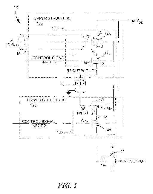
[0013] FIG. 1 is a schematic diagram of two-stage pair CMOS amplifier circuit
according
to the disclosure;
[0014] FIG. 2 shows the arrangement of FIGS. 2A and 2B which taken together is
a
diagrammatical, cross sectional sketch of the two-stage pair CMOS amplifier
circuit of
FIG. 1 according to the disclosure; and
[0015] FIGS. 3A-3H are diagrammatical, cross sectional sketches of a portion
of the two-
stage pair CMOS amplifier circuit of FIGS. 1 and 2 at various stages in the
fabrication
thereof at various stages in the manufacturing process thereof according to
the disclosure;
FIG. 3D' being an exploded view of a portion of the structure shown in FIG.
3D; FIG.
3D' being atop view of such portion of FIG. 3D; FIGS. 3G' being an exploded
view of a
portion of the structure shown in FIG. 3G; FIG. 3G" being a top view of FIG.
3G' and
FIG. 3G" being a bottom view of FIG. 3G'.
[0016] Like reference symbols in the various drawings indicate like elements.
4
CA 03031756 2019-01-23
WO 2018/075099
PCT/US2017/037462
DETAILED DESCRIPTION
[0017] Referring now to FIG. 1, a schematic diagram of two-stage pair CMOS
amplifier
circuit 10 is shown to include a first stage CMOS circuit 10a having an output
coupled to a
second stage CMOS circuit 10b, as shown. Each one of the CMOS circuits 10a,
10b is
formed on a corresponding one of a pair stacked, directly bonded structures
12a, 12b,
respectively, as shown; an upper structure (layer 1) 12a and a lower structure
(layer 2) 12b.
The first stage CMOS circuit 10a include: an nMOS FET 14a having a gate (G)
fed by an
RF input signal through a coaxial transmission line 16, sometimes also
referred to as coax,
to 16; a drain (D) connected to a Vdd voltage supply and a source (S)
connected to the drain
(D) of an pMOS FET 14b, as shown. The gate (G) of the pMOS FET 14b is fed by a
control signal input 1, as indicated. The source of the nMOS FET 14a provides
the output
for the first stage CMOS circuit 10a and is connected through a coaxial
transmission line
18, sometimes also referred to as coax, 18. The coaxial transmission line 18
is connected
to the input of the second stage CMOS circuit 10b. More particularly, here the
source of
nMOS FET of circuit 10a is coupled to the gate (G) of a nMOS FET 14c of
circuit 10b
through the coaxial connector 18, as shown. The drain (D) of the nMOS FET 14c
of circuit
10b is connected to Vdd, as shown, and the source (S) is connected to the
drain (D) of the
nMOS FET 14d of circuit 10b, as shown. The Gate (G) of nMOSFET 14d is
connected to
a control signal input 2, as shown, and the source (S) of the nMOS FET 14d of
circuit 10b
provides the RF output of the two stage amplifier circuit 10, such output
being coupled
through a coaxial transmission line 20, sometimes also referred to as coax,
20, as shown. It
is noted that the bodies of the n-channel transistors of the first and second
circuits 10a and
10b are connected to ground and the bodies of the p-channel transistors are
tied to Vdd, as
shown. Alternatively, the transistor bodies can be tied to the source
connection as
commonly done on SOI analog circuits. It should also be noted that a coaxial
transmission
lines 16, 18 and 20 each an inner electrical conductor 16c, 18c and 20c,
respectfully, and a
grounded outer electrically conductive shield structure 16o, 18o and 20o,
respectively,
disposed around the inner electrical conductors 16c ,18c, and 20c,
respectively, as
indicated. Here, in this example, as will be described, outer electrically
conductive shield
structure has a plurality of spaced electrical conductors separated one from
another by
less than one-quarter wavelength of the operating wavelength of the coaxial
transmission
line and thus provides an electrically continuous conductor for the outer
conductor shield
5
CA 03031756 2019-01-23
WO 2018/075099
PCT/US2017/037462
structure. It should be understood, however, that the outer electrically
conductive shield
structure may be a continuous electrical conductor.
[0018] Referring now to FIGS. 2, 2A and 2B, a diagrammatical, cross sectional
sketch of
the two-stage pair CMOS amplifier circuit 10 is shown. It is first noted that
one portion of
the coaxial transmission line 18, portion 18a is formed in the bottom portion
of layer 12a
and another portion 18b is formed in the upper portion of layer 12b. It is
also noted that
connections to the outer electrically conductive shield structures of the
coaxial
transmission lines 16, 18 and 20 are interconnected by vertical conductive
vias, to be
described, as well as by an out-of-plane ground bus 22 and are connected to
ground, as
indicated.
[0019] Referring now to FIGS. 3A-3H, a portion of an integrated circuit having
formed
therein one of the pair of CMOS circuits 10, here circuits 10a, is shown in
FIG. 3A. The
circuit 10a is formed using a conventional SOI front end of line (FEOL) handle
30; here
for example a silicon wafer. The FEOL structure 11 includes a BOX layer 32,
here silicon
dioxide, is formed on the upper surface of the handle 30. A layer 34 of
silicon is formed
on the BOX layer 32; the silicon layer 34 suitably doped to form therein the
nMOS
transistor 14a and the pMOS transistor 14b using conventional processing. A
gate oxide
layer 38 is formed on portions of the silicon layer 34, as shown, using any
conventional
technique. Gate (G) electrodes 40 are formed over gate oxide layer 28 of the
nMOS and
pMOS transistors 12a, 12b, respectively as shown, using conventional
photolithographic-
etching processing.
[0020] Next, referring to FIG. 3B, the CMOS transistors 14a, 14b are
electrically insulated
from each other and from other portions and electrical elements by deep trench
isolation
(DTI) region 36, here Plasma Enhanced Chemical Vapor Deposition (PECVD)
Tetraethylorthosilicate (TEOS), using conventional processing, as shown; the
deep trench
isolation region 36 extend from the top of the silicon layer 34 down to the
BOX layer 32.
It is noted that the deep trench isolation material 36 has a lower
permittivity than the
permittivity of the silicon 34. Here, the relative permittivity of the TEOS is
3.9 and the
relative permittivity of the silicon layer 34 is 11.9. Thus, having the
coaxial transmission
line 18a (FIG. 2) pass through a lower permittivity DTI 36 rather than passing
through the
silicon layer 34 there will be less signal transmission loss when passing
through the DTI
6
CA 03031756 2019-01-23
WO 2018/075099
PCT/US2017/037462
layer 36 than the silicon layer 34 because the DTI 36 will provide a
dielectric between
inner conductor and the outer conductor shield structure. Further, the use of
a coaxial
transmission line that passes through the DTI material 36 enables use of very
thin silicon
layer 34 in order to maximize functional density of the integrated circuit
formed in the
silicon layer and minimizes losses through the vias by placing the coaxial
transmission
lines 18, 20 in an oxide ((DTI) material 36) having very low conductivity and
loss tangent
compared with silicon. Use of SOT simplifies construction of the structure
which
simplifies integration into integrated 3D RF Devices. A passivation layer,
dielectric layer
44, here for example, silicon nitride, is formed over the DTI region 36, as
shown in FIGS.
to 3B.
[0021] Next, referring to FIG. 3C, a portion 18a' of the coaxial transmission
line 18 is
formed. First, a plurality of electrically conductive vias 18'o is formed in
predetermined
pattern here in a circular array of conductive vias with a central conductive
via 18'c using
photolithographic-etching techniques; here Reactive Ion Etching. Then the via
openings
are filled with tungsten using CVD to form the inner, or center, electrical
conductor 18'c
and the outer electrically conductive shield structure 18'o; the outer
electrically conductive
shield structure 18'o being here formed as a circular array of rod-like
electrical conductors
18" as shown in FIG. 3C' which shows atop view of the section shown in FIG.
3C.
[0022] Next, referring to FIG. 3D, a first electric interconnect dielectric
(ILD) structure
48, here silicon dioxide, is formed to provide: electrical vias 41o, 41c
having contact pads
41'o, 41'c, connected to the electrical conductors 18'o, 18c', respectively as
shown, of the
portion 18a' of the coaxial transmission line 18; electrical vias 43 to the
source and drain
regions of the CMOS transistors 14a, 14b; a ground via 42 for connection to
ground and
corresponding vias in layer 2 12b, to be described; a Vdd conducive via 46 for
FETs 14a,
and 14c, described above in FIG. 1; conductive vias 45, having contact pads
45', to the
gates (G) of FETS 14a, 14b; an electrical vias 46 for connection to the gate G
of FET 14c,
to be described; and an electrical interconnect 47 connecting the source of
FET 14 b to the
.. conductive via 41 that is connected to the center conductor 18'c of the
coaxial
transmission line 18; and an electrical connector 59 for connecting Vdd to the
drain of
FET 14a. Also formed is an out-of-plane conductor 51 for connection to the
ground bus
22 (FIG. 2).
7
CA 03031756 2019-01-23
WO 2018/075099
PCT/US2017/037462
[0023] Next a second electric interconnect dielectric (ILD) structure 50, here
silicon
dioxide, is formed to provide: a coax ground pad 62 for the coaxial
transmission line 16
which is connected to a circular array of vertical conductive vias 63 for the
coaxial
transmission line 16; the center conductor 65 for the coaxial transmission
line 16; an
electric connector 60 for connecting the center conductor 18c of the coaxial
transmission
line 18 to the source of FET 14b though vias 74, as shown; via 70 connected to
via 42; via
72 connected to via 46 and vias 43 and interconnect 43 for connecting the
source and
drains of FETs 14a and 14b as shown. It is noted that contact pad 64o is a
generally
square or rectangular shaped pad having a central aperture for the contact pad
65 (FIG.
.. 3D').
[0024] Next, in FIG. 3E, a bonding oxide 76 is formed over the upper surface
of the
structure 70 (which includes the FEOL structure 11, the first ILD structure 48
and the
second ILD structure 50, as shown in FIG. 3D) is bonded to a new handle 73
here for
example using bonding oxide layer 76 after which the first handle 30 is
removed as shown
(FIG. 3F) exposing the bottom of structure 70, as shown.
[0025] Next, with the first handle 30 removed, FIG. 3G shows metal pads 84a,
84b, 84o,
84c and 84d are formed on portions of the exposed BOX layer 32 under the
exposed ends
of the electrically conductive vias 42, 72, 18`o, 18'c, and 44, as shown, to
produce
contacts for vias 42, 72, 18`o, 18'c, and 44 where contact 84o and 84c provide
then
contacts to the outer conductor and center conductor, respectively, of coaxial
transmission
line 18, as indicated. Here, the metal pads for the upper portion of the
coaxial connector
18 are indicated as 84o for the outer conductor and 84c for the center
conductor. FIG. 3G'
shows a diagrammatical cross-sectional view of a portion of the structure from
the top of
layer 50 to the bottom of BOX 32; the top view being shown in FIG. 3G" and the
bottom
view being shown in FIG. 3G". It is noted that the contact pad 41o' is a pad
having a
central aperture 53 for the contact pad 41c and. likewise, contact pad 84o is
a pad having a
central aperture 85 for the contact pad 84c.
[0026] Next, the lower structure 12b (FIGS 2, 2A and 2B) is shown in FIG. 3H
is formed
in like manner. The two structures 12a, 12b are aligned (with, for example
contact pads
84a, 84b, 84c, 84o and 84d of structure 12a are aligned with contact pads
84'a, 84'b,
84'o, and 84'd, respectively; as shown in FIGS. 2, 2A and 2B and then
structures 12a and
8
CA 03031756 2019-01-23
WO 2018/075099
PCT/US2017/037462
12b and bonded together to produce the structure shown in FIGS. 2, 2A and 2B.
This bond
can be formed using a variety of methods including adhesive, anodic, thermo-
compressive, or oxide bonding with electrical connection between metal pads
84a to 84'a
and 84b to 84'b. It is noted that contact pad 84'o is a pad 84o having a
central aperture for
the contact pad 84'c.
[0027] It should now be appreciated, a semiconductor structure according to
the disclosure
includes: a bottom oxide insulating layer; a silicon layer disposed on the
bottom oxide
insulating layer; a deep trench isolation (DTI) material passes vertically
through the
silicon layer to the bottom oxide insulating layer, the deep trench isolation
material having
a lower permittivity than the permittivity of the silicon layer; and a coaxial
transmission
line having an inner electrical conductor and an outer electrically conductive
shield
structure disposed around the inner electrical conductor passing vertically
through the
deep trench isolation material to electrically connect electrical conductors
disposed over
the bottom oxide insulating layer to electrical conductors disposed under the
contacts
bottom oxide insulating layer.
[0028] It should now also be appreciated, a semiconductor structure according
to the
disclosure includes: a bottom oxide insulating layer; a silicon layer disposed
on an upper
surface of the bottom oxide insulating layer; wherein the silicon layer a deep
trench
isolation material passing vertically through the silicon layer to the bottom
oxide
insulating layer; a dielectric structure disposed over the silicon layer; a
plurality of
electrical contacts disposed on the dielectric structure, a first portion of
the electrical
contacts being electronically connected electrically conductive vias passing
vertically
through the dielectric structure, and a second portion of the electrical
contacts being
electrically being connected to electrical contacts disposed on a bottom
surface of the
bottom oxide insulating layer by a plurality of spaced electrically conductive
vias passing
vertically through the dielectric structure, the deep trench isolation
material, and the
bottom oxide layer; and wherein the plurality of spaced electrically
conductive vias
connected to the second portion of the electrical contacts are arranged to
provide a coaxial
connector between the second portion of the electrical contacts and the
electrical contacts
disposed on a bottom surface of the bottom oxide insulating layer.
9
CA 03031756 2019-01-23
WO 2018/075099
PCT/US2017/037462
[0029] It should now also be appreciated, a semiconductor, silicon-on-oxide
(SOT)
structure according to the disclosure includes: a bottom oxide (BOX)
insulating layer; a
silicon layer disposed on the bottom oxide (BOX) insulating layer; a deep
trench isolation
(DTI) material passing vertically through the silicon layer to the bottom
oxide insulating
layer, the deep trench isolation material having a lower permittivity than the
permittivity
of the silicon; wherein the silicon layer has formed therein a pair of
complementary metal
oxide semiconductor (CMOS) transistors, the transistor being electrically
isolated one
from the other by the deep trench isolation (DTI) material; and a coaxial
transmission line
having an inner electrical conductor and an outer electrically conductive
shield structure
disposed around the inner electrical conductor passing vertically through the
deep trench
isolation material to electrically connect electrical conductors disposed over
the bottom
oxide insulating layer to electrical conductors disposed under the contacts
bottom oxide
insulating layer. The semiconductor SOT structure may include one or more of
the
following features independently or in combination with another feature to
include:
.. wherein the inner conductor and outer the outer conductor shield structure
are chemically
vapor deposited (CVD) tungsten or wherein the outer conductor shield structure
comprises
a plurality of spaced electrical conductors separated one from another by less
than one-
quarter wavelength of the operating wavelength of the coaxial transmission
line and thus
provides an electrically continuous conductor for the outer conductor shield
structure.
[0030] A number of embodiments of the disclosure have been described.
Nevertheless, it
will be understood that various modifications may be made without departing
from the
spirit and scope of the disclosure. For example, other metals may be used in
place of
tungsten, such as, for example, copper and tantalum. Further the conductive
vias passing
through the DTI material 36 may be hollow tube rather than solid rods.
Accordingly, other
embodiments are within the scope of the following claims.