Note: Descriptions are shown in the official language in which they were submitted.
85071069
- 1 -
'DEVICE AND METHOD TO STABILIZE A SUPPLY VOLTAGE
CROSS REFERENCE TO RELATED APPLICATIONS
[0001] The present application claims priority to U.S. Patent Application No.
15/272,110 filed on September 21, 2016, later published as U.S. Patent
Publication
No. 20180083533.
FIELD
[0002] The present disclosure is generally related to devices and methods to
stabilize
a supply voltage.
DESCRIPTION OF RELATED ART
[0003] Advances in technology have resulted in smaller and more powerful
computing devices. For example, a variety of portable personal computing
devices,
including wireless telephones, such as mobile and smart phones, tablets and
laptop
computers are small, lightweight, and easily carried by users. These devices
can
communicate voice and data packets over wireless networks. Further, many such
devices incorporate additional functionality, such as a digital still camera,
a digital
video camera, a digital recorder, and an audio file player. Also, such devices
can
process executable instructions, including software applications, such as a
web
browser application, that can be used to access the Internet. As such, these
devices
can include significant computing and networking capabilities.
[0004] To reduce voltage fluctuations, such devices include processor cores
that
utilize voltage regulators. A voltage regulator may be a simple feed-forward
design
or may include negative feedback control loops. Depending on the design, the
voltage regulator may be used to regulate one or more alternating current (AC)
or
direct current (DC) voltages. Voltage regulators, such as buck regulators, may
exhibit
unacceptable voltage "droop" due to sharp steps in load current. For example,
when a
processor core "powers up," a large load current may cause a supply voltage to
drop
until the voltage regulator can provide sufficient current to stabilize the
voltage.
Large voltage droop may cause the regulated supply voltage to fall below
minimum
required levels for circuit operation.
CA 3033955 2020-04-08
85071069
- 2 -
SUMMARY
[0005] According to one implementation of the present disclosure, an apparatus
to stabilize a
supply voltage includes a first current source, a second current source, and a
control circuit.
The first current source is responsive to a detection signal and has an output
coupled to a
voltage regulator circuit via an output node. The second current source is
also coupled to the
output node. The control circuit includes an input responsive to the detection
signal and an
output coupled to the second current source. The control circuit is configured
to enable the
second current source based on a delayed version of the detection signal.
[0006] According to another implementation of the present disclosure, a method
includes
receiving a detection signal at a control circuit. The detection signal
indicates that an output
voltage of a voltage regulator circuit is below a threshold voltage. The
method also includes
enabling a first current source that is responsive to the detection signal and
enabling a second
current source responsive to a delayed version of the detection signal.
[0007] According to another implementation of the present disclosure, an
apparatus includes
means for providing a first current to an output node. The means for providing
the first current
is responsive to a detection signal and is coupled, via an output node, to a
means for
regulating a voltage at the output node. The apparatus also include means for
providing a
second current to the output node. The apparatus further includes means for
enabling the
means for providing the second current based on a delayed version of the
detection signal.
[0008] According to another implementation of the present disclosure, a non-
transitory
computer-readable medium includes instructions that, when executed by a
processor, cause
the processor to perform operations including enabling a first current source
responsive to a
detection signal. The detection signal indicates that an output voltage of a
voltage regulator
circuit is below a threshold voltage. The operations also include enabling a
second current
source responsive to a delayed version of the detection signal.
[0008a] According to another implementation of the present disclosure, there
is provided an
apparatus comprising: a first current source responsive to a detection signal
and having an
output coupled to an output node of a voltage regulator circuit; a second
current source
CA 3033955 2020-04-08
85071069
- 2a -
coupled to the output node of the voltage regulator circuit; and a control
circuit having an
input responsive to the detection signal and an output coupled to the second
current source,
the control circuit configured to enable the second current source based on a
delayed version
of the detection signal, and wherein the first and second current sources are
configured to
adjust a first current and a second current based on a headroom voltage of the
voltage
regulator circuit such that the first and second currents increase responsive
to a decrease in the
headroom voltage of the voltage regulator circuit.
[00081)] According to another implementation of the present disclosure, there
is provided a
method comprising: receiving a detection signal at a control circuit, the
detection signal
indicating that an output voltage of a voltage regulator circuit is below a
threshold voltage;
enabling a first current source responsive to the detection signal; and
enabling a second
current source responsive to a delayed version of the detection signal, and
wherein the first
and second current sources are configured to adjust a first current and a
second current based
on a headroom voltage of the voltage regulator circuit such that the first and
second currents
increase responsive to a decrease in the headroom voltage of the voltage
regulator circuit.
10008c1 According to another implementation of the present disclosure, there
is provided an
apparatus comprising: means for providing a first current to an output node,
the means for
providing the first current responsive to a detection signal and coupled, via
an output node, to
a means for regulating a voltage at the output node; means for providing a
second current to
the output node; and means for enabling the means for providing the second
current based on
a delayed version of the detection signal, and wherein the first and second
current sources are
configured to adjust a first current and a second current based on a headroom
voltage of the
voltage regulator circuit such that the first and second currents increase
responsive to a
decrease in the headroom voltage of the voltage regulator circuit.
CA 3033955 2020-04-08
CA 03033955 2019-02-14
WO 2018/057112
PCT/US2017/044085
- 3 -
BRIEF DESCRIPTION OF THE DRAWINGS
[0009] FIG. 1 is a diagram of a system that is operable to reduce output
voltage
droop.
[0010] FIG. 2 is a circuit diagram of a device to stabilize a supply voltage
that may be
included in the system of FIG. 1.
[0011] FIG. 3 is a diagram of another illustrative example of a device to
stabilize a
supply voltage.
[0012] FIG. 4 is a diagram of an illustrative example of a current source of a
device to
stabilize a supply voltage.
[0013] FIG. 5 is a method for providing current to an output node of a voltage
regulator circuit.
[0014] FIG. 6 is a block diagram of a device that may include components that
are
operable to reduce output voltage droop.
DETAILED DESCRIPTION
[0015] Particular implementations of the present disclosure are described
below with
reference to the drawings. In the description, common features are designated
by
common reference numbers throughout the drawings.
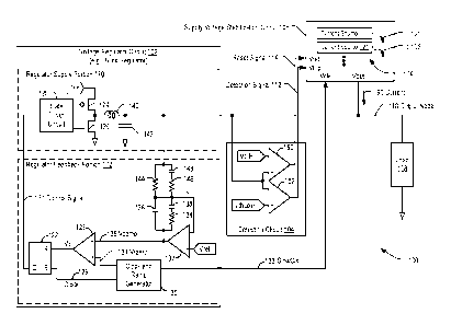
[0016] Referring to FIG. 1, a system 100 that is operable to reduce output
voltage
droop is shown. The system 100 includes a voltage regulator circuit 102, a
detection
circuit 104, a supply voltage stabilization circuit 106, and a load 108. The
voltage
regulator circuit 102 may be configured to regulate a voltage at an output
node 110.
The supply voltage stabilization circuit 106 may be configured to quickly ramp
up a
current 190 to the output node 110 in response to a sudden drop of the voltage
at the
output node 110. For example, when a load current through the load 108
increases
faster than the transient response of the voltage regulator circuit 102 can
accommodate the increased load current, the voltage at the output node 110
drops. In
response to the voltage drop, the supply voltage stabilization circuit 106 may
increase
CA 03033955 2019-02-14
WO 2018/057112
PCT[US2017/044085
- 4 -
the current 190 until the voltage at the output node 110 is stabilized and may
then
ramp down the current 190 as the voltage regulator circuit 102 adapts to the
increased
load current. The supply voltage stabilization circuit 106 is also referred to
herein as
an asynchronous transient response accelerator (ATRA) 106.
[0017] The voltage regulator circuit 102 may include a regulator supply
portion 170
that is coupled to the output node 110 and that is responsive to a control
signal 137
from a regulator feedback portion 172. In some implementations, the voltage
regulator circuit 102 may include or correspond to a buck regulator.
[0018] The regulator supply portion 170 includes a gate driver circuit 120
that is
coupled to a gate of a pull-up transistor 124 and a gate of a pull-down
transistor 126.
A first terminal of an inductor 140 is coupled to the drains of the
transistors 124, 126,
and a second terminal of the inductor 140 is coupled to the output node 110. A
first
terminal of a capacitor 142 is coupled to the output node 110, and a second
terminal
of the capacitor 142 is coupled to ground.
[0019] The gate driver circuit 120 is configured to selectively activate and
deactivate
each of the transistors 124, 126 responsive to the control signal 137. For
example, the
gate driver circuit 120 may be configured to couple the inductor 140 to a
supply
voltage (Vin) while the control signal 137 has a first voltage level (e.g., a
logical high
voltage) by activating the pull-up transistor 124 and deactivating the pull-
down
transistor 126, and to couple the inductor 140 to ground while the control
signal 137
has a second voltage level (e.g., a logical low voltage) by deactivating the
pull-up
transistor 124 and activating the pull-down transistor 126.
[0020] The regulator feedback portion 172 is coupled to the output node 110
and
configured to generate the control signal 137 as a pulse-width modulation
(PWM)
signal having a duty cycle based on the voltage at the output node 110. The
regulator
feedback portion 172 includes an error amplifier 132 for the voltage generator
circuit
102 that is configured to generate a voltage (Vcomp) 135 based on a difference
between a first voltage (Vi) and a reference voltage (Vref). A resistor 134
and
capacitors 136, 138, in conjunction with resistors 144, 146 and a capacitor
148, are
CA 03033955 2019-02-14
WO 2018/057112
PCT[US2017/044085
- 5 -
compensation components configured to implement a Type III compensation
network
for the error amplifier 132.
[0021] The voltage regulator circuit 102 also includes a comparator circuit
128, a
clock and ramp generator 130, and a pulse-width modulation (PWM) latch 122. A
first input terminal of the comparator circuit 128 is coupled to receive a
ramp voltage
(Vramp) 131 generated by the clock and ramp generator 130, and a second input
terminal of the comparator circuit 128 is coupled to receive Vcomp 135 from
the error
amplifier 132. Vramp 131 may have a voltage level that increases from a low
voltage
level and resets (to a low voltage level) after reaching a high voltage level.
Thus,
Vramp 131 may steadily increase, reset, and repeat in a continuous manner.
[0022] The comparator circuit 128 may generate a pulse width modulated signal
(V2)
by outputting a low voltage while the ramping voltage Vramp 131 is less than
Vcomp
135 and transitioning to a high voltage when Vramp 131 exceeds Vcomp 135. The
PWM latch 122 is responsive to the output (V2) of the comparator circuit 128
and a
clock signal 129 from the clock and ramp generator 130 and may include a set-
reset
(S-R) flip-flop configured to output the control signal 137. As an
illustrative example
of operation, the clock signal 129 may first set the PWM latch 122, which then
turns
on the pull-up transistor 124. The Vramp signal 131 may start increasing from
its
lowest value simultaneous (e.g., at least partially overlapping in time) to
the PWM
latch 122 being set. In response to the voltage of Vramp 131 rising above
Vcomp
135, the output V2 of the comparator circuit 128 transitions to a logical high
voltage.
The transition of the output V2 resets the PWM latch 122, which turns off the
pull-up
transistor 124 and turns on the pull-down transistor 126. The error amplifier
132
slowly adjusts Vcomp 135 (slowly relative to how fast the Vramp signal 131
slews) to
produce a PWM duty cycle that results in the voltage at the output 110 being
approximately equal to (or equal to) the reference voltage Vref.
[0023] The detection circuit 104 may also be referred to as a "droop
comparator".
The detection circuit 104 includes a comparator circuit 150 and a comparator
circuit
152. The output node 110 is coupled to a first input terminal of the
comparator circuit
CA 03033955 2019-02-14
WO 2018/057112
PCT/US2017/044085
-6-
150 and to a second input terminal of the comparator circuit 152. A second
input
terminal of the comparator circuit 150 is coupled to receive a threshold
voltage
(VthHi) (e.g., a "high" threshold voltage), and a first input terminal of the
comparator
circuit 150 is coupled to receive another threshold voltage (VthLow) (e.g., a
"low"
threshold voltage). The comparator circuit 152 is configured to generate a
detection
signal 112 (e.g., output a logical high voltage) in response to the voltage at
the output
node 110 being less than VthLow. The comparator circuit 152 may be configured
to
generate a reset signal 114 (e.g., output a logical high voltage) in response
to the
voltage at the output node 110 being greater than VthHi.
[0024] The ATRA 106 may be coupled to receive the detection signal 112 and the
reset signal 114 from the detection circuit 104 and to receive a clock signal
(SlowC1k)
133 from the clock and ramp generator 130. The ATRA 106 includes multiple
current sources 109 including a first current source 111 and a second current
source
121. In an illustrative implementation, the current sources 109 (e.g., the
first current
source 111 and the second current source 121) include p-type metal oxide
semiconductor (PMOS) transistors.
[0025] The ATRA 106 may be configured to sequentially activate the current
sources
109 in response to the detection signal 112. For example, the first current
source 111
is configured to generate a first current Ii 191 in response to a detection
signal, such
as the detection signal 112 indicating that the voltage at the output node 110
is less
than VthLow. The second current source 121 is configured to generate a second
current 12 192 in response to a delayed version of the detection signal. For
example,
the delayed version of the detection signal may be generated by a delay
element, such
as one or more buffers, that is responsive to the detection signal, as
described in
further detail with reference to FIG. 2. The multiple current sources 109 may
include
one or more additional current sources (not shown) that are each configured to
generate a respective current in response to one or more other delayed
versions of the
detection signal. The combined current (if any) from the multiple current
sources 109
is provided as the current 190 to the output node 110. Example implementations
of
the ATRA 106 are described in further detail with reference to FIGs. 2-4.
CA 03033955 2019-02-14
WO 2018/057112
PCT/US2017/044085
-7-
100261 The ATRA 106 may be configured to deactivate the multiple current
sources
109 based on a clock signal, such as the clock signal 133 received from the
clock and
ramp generator 130. For example, the ATRA 106 may be configured to continue
sequentially activating additional current sources, increasing the current
190, while
the detection signal 112 indicates that the voltage at the output node 110 is
less than
VthLow. In response to the detection signal 112 indicating that the voltage at
the
output node 110 has risen above VthLow, the ATRA 106 may be configured to
cease
activating additional current sources and may begin sequentially deactivating
the
current sources that are activated, decreasing the current 190 in a series of
steps that
may correspond to cycles of the clock signal 133.
[0027] During operation, the voltage at the output node 110 may be held at a
substantially constant voltage level by the voltage regulator circuit 102
during a
steady-state operation. The signals 112, 114 of the detection circuit 104 may
indicate
that the voltage at the output node 110 is not below VthLow and is not above
VthHi
(e.g., the detection signal 112 and the reset signal 114 are both logical low
voltages).
The current sources 109 of the ATRA 106 are deactivated and substantially no
current
flows from the output terminal (Vout) of the ATRA 106 to the output node 110.
[0028] A sudden increase in the load current that is provided to the load 108
may
disrupt the steady-state operation. For example, the load 108 may include one
or
more processor cores that transition from a low-power mode to an active mode,
such
as multiple cores that transition to the active mode at substantially the same
time. The
sudden increase in load current drains charge from the capacitor 142 of the
voltage
regulator circuit 102 and lowers the voltage at the output node 110 more
quickly than
the regulator feedback portion 172 can adjust the control signal 137 to
provide
additional current to the output node 110. When the voltage at the output node
110
falls below VthLow, the detection circuit 104 generates the detection signal
112
indicating the voltage drop (e.g., transitions the detection signal 112 from a
logical
low voltage to a logical high voltage).
[0029] The ATRA 106 may respond to the detection signal 112 indicating the
voltage
drop by sequentially activating current sources of the multiple current
sources 109.
CA 03033955 2019-02-14
WO 2018/057112
PCT[US2017/044085
- 8 -
For example, the ATRA 106 may activate the current source 111 to provide the
current II 191 as the current 190 to the output node 110. After a short delay,
if the
detection signal 112 continues to indicate the voltage drop, the ATRA 106 may
activate the second current source 121 to provide the combined current 1i 191
+12
192 as the current 190 to the output node 110. The ATRA 106 may continue to
activate additional current sources to increase the current 190 to the output
node while
the detection signal 112 indicates the voltage drop. As a result, the output
current 190
may increment or "ramp up" in a series of steps of increasing current as more
of the
current sources 109 are activated. The output current 190 may contribute to
the load
current provided to the load 108, may contribute to recharging the capacitor
142, or a
combination thereof
[0030] When the detection circuit 104 detects that the voltage at the output
node 110
is not lower than VthLow, the detection circuit 104 adjusts the detection
signal 112
(e.g., by transitioning the detection signal 112 from a logical high voltage
to a logical
low voltage). The ATRA 106 may respond to the detection signal 112 indicating
that
the voltage at the output node 110 is not lower than VthLow by halting the
sequential
activation of current sources. Current sources that have been activated remain
activated, while inactive current sources remain inactive. As a result, the
current 190
may be substantially unchanged immediately after the transition of the
detection
signal 112. The ATRA 106 may begin deactivating the current sources at a
slower
rate than the ATRA 106 activated the current sources. The rate of deactivating
the
current sources may be based on an estimated or predicted speed of the voltage
regulator circuit 102 to adjust for the changes in current resulting from
deactivation of
the current sources.
[0031] Under some conditions the voltage at the output node 110 may exceed
VthHi.
For example, the load 108 may include a processor core that transitions from a
low
power mode to an active mode and then quickly transitions back to the low
power
mode. In response to the increased load current resulting from the processor
transition to the active mode, the ATRA 106 quickly ramps up the current 190.
Upon
the processor transitioning back to the low-power mode, the current 190
provided by
CA 03033955 2019-02-14
WO 2018/057112
PCT[US2017/044085
- 9 -
the ATRA 106 is no longer consumed by the load 108 and instead may charge the
capacitor 142, driving the voltage at the output node 110 above VthHi. In
response to
the reset signal 114 indicating that the voltage at the output node 110
exceeds VthHi,
the ATRA 106 may deactivate all of the current sources 109 substantially
simultaneously (rather than sequentially based on the clock signal 133) to
terminate
the current 190.
[0032] The system 100 of FIG. 1 may thus utilize the ATRA 106 to provide
current to
the output node 110 in response to a sudden voltage drop at the output node
110. The
ATRA 106 may respond more quickly to the voltage drop than the voltage
regulator
circuit 102 and provides current 190 to the output node 110, reducing the
amount of
current 190 as the voltage regulator circuit 102 adjusts to accommodate the
increased
current of the load 108 that caused the voltage drop. For example, the ATRA
106
may provide appropriate "on-die" current supply to prevent unacceptable droop
to
sharp "steps" in load current without creating undesired noise to the output
voltage of
the voltage regulator circuit 102 and while efficiently moving the load
current to the
voltage regulator circuit 102. Thus, the ATRA 106 may prevent digital circuits
(e.g.,
a processor core) from "crashing" or falling below minimum required levels for
improved circuit operation. Further, by providing a quick response to voltage
drops,
the ATRA 106 may enable the system 100 to be designed using a smaller, on-die
capacitor 142 to reduce an overall cost and size of the system 100 as compared
to
systems that use a large, off-chip capacitor to accommodate sharp steps in
load
current.
[0033] To illustrate, a relation between the maximum load current step, the
output
capacitance of the voltage regulator 102, and the delay times to activate the
current
sources 109 (e.g., the delay of the comparator circuit 152 and of delay
buffers in the
ATRA 106) may be used during design of the system 100, such as when
determining
a size (e.g., capacitance) of the load capacitor 142. For example, one
estimate for
determining a size of the load capacitor 142 may be expressed as Cload >=
Iload *
Tdelay * N / (VthLow ¨ Vmin0p), where Iload is the largest load current step,
Tdelay
is the delay of the comparator circuit 152 and the delay buffers of the ATRA
106, N is
the number of current sources or stages in the ATRA 106 (described in further
detail
CA 03033955 2019-02-14
WO 2018/057112
PCT/US2017/044085
- 10 -
with reference to FIGs. 2-3), and VminOp is the minimum (e.g., lowest)
allowable
voltage level for the output voltage Vout of the voltage regulator circuit
102.
[0034] Although the voltage regulator circuit 102 is described as including a
buck
regulator, in other implementations the voltage regulator circuit 102 may
include any
other type of voltage regulator. Although the ATRA 106 is depicted as
including two
current sources 109, the ATRA 106 may be implemented using three, four, ten,
or any
other number of current sources 109. Although the clock signal 133 is depicted
as
generated by the clock and ramp generator 130, in other implementations the
clock
signal 133 may be generated by another component (such as a ring oscillator
circuit)
within or external to the ATRA 106. In some implementations, the clock signal
133
may be omitted, such as in an implementation where activated current sources
are
deactivated based on another signal. For example, activated current sources
may be
deactivated based on deactivation of the detection signal 112 (e.g., when the
voltage
at the output node 110 rises above VthLow), based on activation of the reset
signal
114, or based on one or more other signals (not shown). To illustrate, all
activated
current sources may be deactivated responsive to a high-to-low voltage
transition of
the detection signal 112. As another example, activated current sources may be
sequentially deactivated based on high-to-low voltage transitions of one or
more
delayed versions of the detection signal 112. Although the detection circuit
104 is
depicted as generating the reset signal 114 and the ATRA 106 is depicted as
responsive to the reset signal 114, in other implementations the reset signal
114 may
be omitted.
[0035] Referring to FIG. 2, a circuit diagram of a particular implementation
of the
ATRA 106 is shown. The ATRA 106 includes the multiple current sources 109 and
a
plurality of control circuits. For example, the ATRA 106 includes the current
source
111, the current source 121, a current source 231, a current source 241, and a
current
source 251. Although five current sources are shown, in other implementations,
the
ATRA 106 may include additional (or fewer) current sources. A control circuit
220 is
coupled to the current source 121, a control circuit 230 is coupled to the
current
source 231, a control circuit 240 is coupled to the current source 241, and a
control
circuit 250 is coupled to the current source 251. Although four control
circuits are
CA 03033955 2019-02-14
WO 2018/057112
PCT[US2017/044085
-11 -
shown, in other implementations, the ATRA 106 may include additional (or
fewer)
control circuits.
[0036] According to some implementations, each current source 111, 121, 231,
241,
251 may include a PMOS transistor. For example, each current source 111, 121,
231,
241, 251 may include a current mirroring type of current source that includes
a PMOS
transistor. Alternatively as illustrated in FIG. 2, each current source 111,
121, 231,
241, 251 may include a PMOS transistor that is operated substantially as a
voltage
controlled resistor. At a given gate-to-source voltage (Vgs) and drain-to-
source
voltage (Vds), a PMOS field effect transistor (FET) can be sized to have a
specific
resistance. Therefore, a PMOS FET can be configured/sized to produce a
specific
amount of drain current. However, if the Vds, or Vheadroom (e.g., Vdd ¨ Vout),
changes, then the drain current also changes. FIG. 4 provides an example of a
circuit
configured to provide substantially constant drain current if Vds or Vheadroom
changes.
[0037] A source of the current source 111 is coupled to a supply voltage
(Vdd), and a
drain of the current source 111 is coupled to the output node 110. The current
source
111 is responsive to the detection signal 112 via an inverter 216 coupled to a
gate of
the current source 111. The inverter 216 may be configured to invert the
detection
signal 112 and provide the inverted signal to the gate of the current source
111. To
illustrate, if the detection signal 112 has a logical high voltage level, the
inverter 216
may provide a signal having a logical low voltage level to the gate of the
current
source 111. In response to receiving the signal having the logical low voltage
level,
the current source 111 may operate as a pull-up transistor that couples the
output node
110 to the supply voltage (Vdd) to generate the first current 11191. As
explained
above, the detection signal 112 may have a logical high voltage level if the
voltage of
the output node 110 is below the threshold voltage (VthLow). Thus, the current
source 111 may operate to provide the first current Ii 191 to the output node
110 if
the voltage of the output node 110 is below the threshold voltage (VthLow).
CA 03033955 2019-02-14
WO 2018/057112
PCT/US2017/044085
- 12 -
[0038] The control circuit 220 includes a delay element 217, a logical NOR
gate 222,
a flip-flop 224, a logical AND gate 226, and a multiplexer (MUX) 228. The
delay
element 217 may be configured to delay the detection signal 112 and to
generate a
first delayed version of the detection signal 202. For example, the delay
element 217
may include one or more serially coupled buffers, inverters, or a combination
thereof.
[0039] The MUX 228 is coupled to receive the first delayed version of the
detection
signal 202 at a first input and the detection signal 112 at a second input. A
control
input of the MUX 228 is coupled to an output (Q) of the flip-flop 224. The MUX
228
is configured to output the first delayed version of the detection signal 202
or the
detection signal 112 based on a value of the control input.
[0040] The AND gate 226 has a first input coupled to the output of the MUX 228
and
has a second input coupled to receive the detection signal 112. An output of
the AND
gate 226 is coupled to an input of the NOR gate 222. The output of the AND
gate 226
is also coupled to a set (S) input of the flip-flop 224.
[0041] The NOR gate 222 has a first input coupled to the AND gate 226 and has
a
second input coupled to the output (Q) of the flip-flop 224. An output of the
NOR
gate 222 is coupled to a control terminal (e.g., a gate) of the current source
121.
[0042] The flip-flop 224 has the set (S) input coupled to the AND gate 226, a
clock
(C) input coupled to receive the clock signal 133, a data (D) input coupled to
an
output of the control circuit 230, and an active-low reset (RB) input coupled
to
receive an inverted version of the reset signal 114 (a "reset bar" signal) via
an inverter
218. The output (Q) of the flip-flop 224 is coupled to the control input of
the MUX
228 and to the NOR gate 222.
[0043] The control circuit 220 is configured to enable (e.g., activate) the
current
source 121 to generate the second current 12 192 based on the first delayed
version of
the detection signal 202. For example, when the output Q of the flip-flop 224,
the
detection signal 112, and the reset signal 114 have a logical low value (LO)
(such that
the active-low reset (RB) input receives a logical high value (HI)), and the
detection
signal 112 transitions from LO to HI, the first delayed version of the
detection signal
CA 03033955 2019-02-14
WO 2018/057112
PCT[US2017/044085
- 13 -
202 transitions from LO to HI after the delay of the delay element 217. The
MUX
228 outputs the first delayed version of the detection signal 202 to provide a
HI signal
to the AND gate 226. Because both inputs to the AND gate 226 are HI, the
output of
the AND gate 226 transitions to HI. The NOR gate 222 responds to the HI output
from the AND gate 226 to activate the current source 121 (via a LO signal at
the gate
of the current source 121). In addition, the HI output from the AND gate 226
received at the S input of the flip-flop 224 sets and holds the output Q at
HI. The
MUX 228 also outputs the first delayed version of the detection signal 202 to
the
control circuit 230.
[0044] The control circuit 230 includes a delay element 227 coupled to receive
the
first delayed version of the detection signal 202 from the control circuit 230
and
configured to generate a second delayed version of the detection signal 204.
The
control circuit 230 also includes a MUX 238, an AND gate 236, a NOR gate 232,
and
a flip-flop 234 that are configured to activate the current source 231 to
provide a
current (13) to the output node 110 responsive to the second delayed version
of the
detection signal 204 in a similar manner as the MUX 228, the AND gate 226, the
NOR gate 222, and the flip-flop 224, respectively, of the control circuit 220
are
configured to activate the current source 121 responsive to the first delayed
version of
the detection signal 202.
[0045] The other control circuits 240, 250 may include similar components and
may
operate in a substantially similar manner as the control circuits 220, 230.
For
example, the control circuit 240 may be configured to enable the current
source 241
based on a third delayed version of the detection signal 206 to provide a
current (14) to
the output node 110. In a similar manner, the control circuit 250 may be
configured
to enable the current source 251 to provide a current (IN ii) to the output
node 110
based on an Nth delayed version of the detection signal (not shown).
[0046] Thus, if the voltage at the output node 110 falls below the voltage
threshold
(VthLow), the detection signal 112 may have a logical high voltage level and
may
cause the current sources 111, 121, 231, 241, 251 to activate in rapid
succession based
on delay times associated with the delay elements 217, 227, etc. In
particular, the
CA 03033955 2019-02-14
WO 2018/057112
PCT[US2017/044085
- 14 -
current source 111 may be configured to provide the current Ii 191 to the
output node
110 in response to the detection signal 112. The current source 121 and the
control
circuit 220 are included in a first incremental current stage 292 that is
configured to
provide the current 12 192 to the output node 110 in response to the first
delayed
version of the detection signal 202. The current source 231 and the control
circuit 230
are included in a second incremental current stage 294 that is configured to
provide
the current 13 to the output node 110 in response to the second delayed
version of the
detection signal 204. The current source 241 and the control circuit 240 are
included
in a third incremental current stage 296 that is configured to provide the
current 14 to
the output node 110 in response to the third delayed version of the detection
signal
206. The current source 251 and the control circuit 250 are included in an Nth
incremental current stage 298 that is configured to provide the current TN+1
to the
output node 110 in response to an Nth delayed version of the detection signal.
[0047] Although four incremental current stages 292-298 are depicted, in other
implementations any number "N" of incremental current stages may be included
in
the ATRA 106, where N may be any integer value greater than zero. As a non-
limiting example, if N is equal to nine, there may be nine incremental current
stages at
the ATRA 106. As illustrated in FIG. 2, each incremental current stage
includes a
respective current source and a respective control circuit that is configured
to provide
an incremental current to the output node 110 in response to a respective
delayed
version of the detection signal 112. As the detection signal 112 propagates
through
the plurality of control circuits (e.g., from the MUX 228 to the delay element
227,
from the MUX 238 to a delay element 237, etc.), the detection signal 112
causes the
corresponding current sources to activate and the corresponding flip-flops to
set (and
store) a logical high voltage level output. By doing so, the current sources
may
provide current to the output node 110. Although in some implementations each
of
the delay elements of the incremental current stages 292-298 applies
substantially
equal delay and each of the current sources 109 generates substantially the
same
amount of current, in other implementations the delay elements may not apply
substantially equal delay, one or more of the current sources 109 may generate
a
CA 03033955 2019-02-14
WO 2018/057112
PCT[US2017/044085
- 15 -
different amount of current (e.g., later-activated current sources may provide
larger
amounts of current than earlier-activated current sources), or a combination
thereof
[0048] If the detection signal 112 switches to a logical low voltage level
(e.g., the
voltage at the output node 110 is no longer less than the voltage threshold
(VthLow)).
the AND gates of the incremental current stages 292-298, responsive to the
detection
signal termination, output logical low values, and the successive activation
of the
current sources 111, 121, 231, 241, 251 stops. As a result, a relatively
stable amount
of current from the activated current sources is provided to the load 108. For
example, the logical high voltage level of the detection signal 112 may cause
incrementing current stages to sequentially activate until the detection
signal 112
switches to a logical low voltage level (e.g., detection signal termination).
After the
detection signal termination, activated current stages may remain activated
(until
deactivated by another mechanism, such as in response to the clock signal 133
or in
response to the reset signal 114, as explained below), and inactive current
stages
remain inactive.
[0049] After the detection signal termination, the activated current stages
may be
sequentially deactivated in responsive to the clock signal 133. In this case,
the clock
signal 133 corresponds to a deactivation clock that sequentially deactivates
current
stages. To illustrate, as each current stage is activated, the output (Q) of
the flip-flop
for that current stage transitions from LO to HI and is provided to the input
(D) of the
flip-flop of the preceding current stage. Non-activated current stages
continue to
output LO to their preceding current stages.
[0050] As an example, if the detection signal 112 transitions to LO after the
incremental current stages 292 and 294 are activated but before the
incremental
current stage 296 is activated, the data (D) input of the flip-flop 234
receives a LO
signal from the inactive current stage 296 and the set (S) input of the flip-
flop 234
receives a LO signal from the AND gate 236. At the next pulse of the clock
signal
133, the output (Q) of the flip-flop 234 transitions from HI to LO,
deactivating the
current source 231 and sending the LO signal to the data (D) input of the flip-
flop 234
of the preceding current stage 292. In response to the next pulse of the clock
signal
CA 03033955 2019-02-14
WO 2018/057112
PCT[US2017/044085
- 16 -
133, the output (Q) of the flip-flop 224 transitions from HI to LO,
deactivating the
current source 121.
[0051] For example, if the current sources 111, 121, 231, 241 are activated,
after the
detection signal termination, the current source 241 may be deactivated. The
current
source 231 may be deactivated after the current source 241 is deactivated, the
current
source 121 may be deactivated after the current source 231 is deactivated, and
the
current source 111 may be deactivated after the current source 121 is
deactivated.
Thus, based on the implementation shown with respect to FIG. 2, the current
sources
241, 231, 121, 111 are turned off from right to left based on a determined
clock period
(e.g., at different time intervals). The clock period may be determined such
that the
voltage regulator circuit 102 has time to absorb the load current increment
supplied by
the deactivated current sources without incurring unacceptable output voltage
droop
(e.g., voltage droop that causes the regulated supply voltage to fall below a
minimum
required level for circuit operation). According to one implementation, the
ATRA
106 may be "retriggerable" such that the current sources may sequentially
activate
(from left to right) if the voltage at the load (e.g., the voltage at the
output node 110)
falls below the threshold voltage (VthLow) again.
[0052] In the implementation of FIG. 2, if the detection signal 112 switches
to a
logical low voltage level prior to all of the flip-flops 224, 234 of the
control circuits
220, 230, 240, 250 being set, the direct Virip input to the logical AND gates
226, 236
that drives the set inputs to the flip-flops 224, 234, as well as the logical
NOR gates
222, 232 that drive the current sources 121, 231, 241, 251, stop any further
setting of
the flip-flops 224, 234 of the control circuits 220, 230, 240, 250. Once a
particular
flip-flop has been set, an output of the particular flip-flop switches the
other input of
the logical AND gate to the detection signal 112 through a multiplexer rather
than
selecting a path through the delay gates. By doing so, the detection signal
112
switches to the logical high voltage level (due to the voltage at the output
node 110
dropping below the threshold voltage (VthLow)) before each flip-flop has been
cleared. Thus, the setting takes place at the next in line un-set flip-flop
without
having to propagate the detection signal 112 through delay gates of set flip-
flops.
CA 03033955 2019-02-14
WO 2018/057112
PCT/US2017/044085
- 17 -
[0053] According to one implementation, the setting of the flip-flops 224, 234
occurs
relatively fast (e.g., "rapidly"). For example, the delay time of the delay
elements
217, 227, 237 are similar to the delay time of the comparator circuit 152 of
FIG. 1.
To illustrate, the delay time of each of the delay elements 217, 227, 237 and
the delay
time of the comparator circuit 152 may be smaller (e.g., e.g., by one or more
orders of
magnitude) than a period of the clock signal 133. The delay time of the delay
elements 217, 227, 237 and the magnitudes of the currents It, 12, 13 etc., may
be set so
that a rate of increase of current provided to the output node 110
substantially matches
an increased load current from the output node 110 under a "worst-case" load
current
scenario (e.g., due to simultaneous activation of multiple processor cores) to
hold the
voltage at the output node 110 at or above a determined voltage level. The
flip-flops
224, 234 of the control circuits 220, 230, 240, 250 may be cleared by clocking
the
control circuit 250 to the control circuit 220 (e.g., clocking from right to
left). The
clock period may be determined such that the voltage regulator circuit 102 has
time to
absorb the current that shifts from deactivating a current source.
[0054] Thus, the comparator circuit 152 generates the detection signal 112
(having a
logical high voltage level), and the current sources 111, 121, 231, 241, 251
(e.g., a
PMOS transistor array) activate in response to the detection signal 112 to
supply extra
current to the load 108. As long as the detection signal 112 has the logical
high
voltage level, the detection signal 112 (including delayed versions thereof)
may
propagate through the plurality of control circuits 220, 230, 240, 250
gradually
activating the current sources 111, 121, 231, 241, 251 and providing
additional
current to the load 108. When enough current is being provided by the PMOS
transistor array to elevate the voltage at the output node 110 above the
threshold
voltage (VthLow), activation of the current sources may stop. After activation
of new
current sources has stopped, the clock signal 133 may gradually clear the flip-
flops
that are "holding on" the activated current sources, thereby providing smaller
increments of current for the voltage regulator circuit 102 to absorb.
[0055] Accordingly, the ATRA 106 of FIG. 2 enables the voltage regulator
circuit
102 to use smaller values for the load capacitance while maintaining
acceptable levels
CA 03033955 2019-02-14
WO 2018/057112
PCT[US2017/044085
- 18 -
of voltage droop at the output node 110. The current sources (e.g., the PMOS
devices) may be used as current shunts that can be scaled linearly or
nonlinearly. In
one example, the PMOS devices that are activated at later stages may be
designed to
be larger in size, and therefore, may provide greater current.
[0056] Referring to FIG. 3, a circuit diagram of another particular
implementation of
the ATRA 106 is shown. One or more features of the ATRA 106 of FIG. 3 may be
as
described with reference to FIG. 1, FIG. 2, or both. For example, in FIG. 3,
the
ATRA 106 includes the control circuits 220, 230. As another example, in FIG.
3, the
ATRA 106 includes the current sources 109, such as the current sources 111,
121,
231, 241, 251.
[0057] In the example of FIG. 3, the ATRA 106 is coupled to receive a second
detection signal 312 (Vtrip2). The second detection signal 312 may be
generated by the
detection circuit 104 of FIG. 1. For example, the detection circuit 104 may be
configured to generate the second detection signal 312 in response to the
voltage at
the output node 110 being below a second threshold voltage (VthLow2) that is
less
than the threshold voltage (VthLow).
[0058] FIG. 3 also illustrates that the ATRA 106 may include one or more NOR
gates
having a three input terminal configuration. For example, the ATRA 106 may
include
a control circuit 340 including a NOR gate 342 having a three input terminal
configuration. As additional examples, the ATRA 106 may include a control
circuit
350 including a NOR gate 352 having a three input terminal configuration and
may
also include a control circuit 360 including a NOR gate 362 having a three
input
terminal configuration. In the example of FIG. 3, the NOR gate 362 includes an
input
coupled to receive the second detection signal 312. One or more additional
components of the control circuits 340, 350 may correspond to one or more
components of the control circuits 220, 230, 240, 250 of FIG. 2.
[0059] The ATRA 106 may also include a control circuit 370 and a control
circuit
380. The control circuit 370 includes a flip-flop 374, an AND gate 376, a
delay
element 377, and a MUX 378. The delay element 377 may be configured to delay
the
CA 03033955 2019-02-14
WO 2018/057112
PCT[US2017/044085
- 19 -
second detection signal 312 and generate a first delayed version of the second
detection signal 302. For example, the delay element 377 may include one or
more
serially coupled buffers (e.g., source follower circuits), inverters, or a
combination
thereof.
[0060] The MUX 378 is coupled to receive the first delayed version of the
second
detection signal 302 at a first input and the second detection signal 312 at a
second
input. A control input of the MUX 378 is coupled to an output (Q) of the flip-
flop
374. The MUX 378 is configured to output the first delayed version of the
second
detection signal 302 or the second detection signal 312 based on a value of
the control
input.
[0061] The AND gate 376 has a first input coupled to the output of the MUX 378
and
has a second input coupled to receive the second detection signal 312. An
output of
the AND gate 376 is coupled to a set (S) input of the flip-flop 374.
[0062] The flip-flop 374 has the set (S) input coupled to the AND gate 376, a
clock
(C) input coupled to receive the clock signal 133, a data (D) input coupled to
an
output of the control circuit 380, and a low-activated reset (R) input coupled
to
receive the reset bar signal (e.g., the inverted version of the reset signal
114 generated
by the inverter 218). A first output (Q) of the flip-flop 374 is coupled to an
input
terminal of the NOR gate 352. A second output (QB) of the flip-flop 374 is
coupled
to an AND gate 318.
[0063] The AND gate 318 includes a first input terminal coupled to receive the
clock
signal 133 and a second input terminal coupled to the flip-flop 374. The AND
gate
318 includes an output terminal coupled to the control circuits 220, 230, 340,
350,
360.
10064] During operation, the second detection signal 312 may enable (e.g.,
activate) a
current source 361. For example, the detection circuit 104 may be configured
to
generate the second detection signal 312 in response to the voltage at the
output node
110 being below a second threshold voltage (VthLow2) that is less than the
threshold
voltage (VthLow). The second detection signal 312 may have a logical high
voltage
CA 03033955 2019-02-14
WO 2018/057112
PCT[US2017/044085
- 20 -
level if the voltage at the output node 110 is less than the second threshold
voltage
(VthLow2). The logical high voltage causes the NOR gate 362 to output a
logical low
voltage to enable the current source 361. The current source 361 may provide a
current to the output node 110.
[0065] The control circuit 370 is configured to enable (e.g., activate) the
current
source 251 to generate a current based on the first delayed version of the
second
detection signal 302. For example, after the second detection signal 312
transitions
from a logical low voltage to a logical high voltage, the delay element 377
may
generate the first delayed version of the second detection signal 302 after
activation of
the current source 361. The first delayed version of the second detection
signal 302
causes the MUX 378 to output a logical high voltage, causing the AND gate 376
and
the first output (Q) of the flip-flop 374 to output logical high voltages. The
logical
high voltage output by the first output (Q) of the flip-flop 374 causes the
NOR gate
352 to output a logical low voltage, enabling (e.g., activating) the current
source 251
to provide a current to the output node 110.
[0066] The control circuit 380 may include similar components and may operate
in a
substantially similar manner as the control circuit 370. For example, the
control
circuit 380 may be configured to enable the current source 241 based on a
third
delayed version of the detection signal 304 to provide a current to the output
node
110.
[0067] Accordingly, the ATRA 106 of FIG. 3 may enable a "meet in the middle"
technique to sequentially activate the current sources 109 to provide current
to the
output node 110. For example, in FIG. 3, the current sources 109 may
sequentially
activate from left to right based on the detection signal 112 (e.g., as
described with
reference to FIG. 2) and may also sequentially activate from right to left
based on the
second detection signal 312. To further illustrate, in FIG. 3, the current
sources 121,
251 may be activated after activation of the current sources 111, 361, and the
current
sources 231, 241 may be activated after activation of the current sources 121,
251. As
a result, the current sources 109 may be activated in a rapid manner, such as
in
CA 03033955 2019-02-14
WO 2018/057112
PCT/US2017/044085
- 21 -
response to the voltage at the output node 110 being below a second threshold
voltage
(VthLow2) that is less than the threshold voltage (VthLow).
[0068] Referring to FIG. 4, a device 400 is shown. In some implementations,
the
device 400 is integrated within the system 100 of FIG. 1. For example, the
device
400 includes a circuit 450 that may be implemented as one or more of the
current
sources 109. In this case, a particular current source of the current sources
109 may
include multiple transistors.
[0069] The device 400 may include one or more resistors, such as resistors
402, 404,
406, and 408. In FIG. 4, the resistor 402 is coupled to receive the voltage at
the
output node 110 to generate a first signal, and the resistor 404 is coupled to
receive
the supply voltage (Vdd) to generate a second signal.
[0070] The device 400 further includes a differential amplifier 412. The
differential
amplifier 412 includes a first input terminal (e.g., an inverting input
terminal) coupled
to receive the first signal from the resistor 402 and further includes a
second input
terminal (e.g., a non-inverting input terminal) coupled to receive the second
signal
from the resistor 404. The differential amplifier 412 is configured to
generate a
headroom voltage Vheadroom based on a difference between the first signal and
the
second signal. The headroom voltage Vheadroom may indicate an amount of
headroom associated with the voltage at the output node 110 and the supply
voltage
(Vdd).
[0071] The device 400 further includes multiple comparator circuits 413, such
as
comparator circuits 414, 416, 418. The multiple comparator circuits 413 are
coupled
to the differential amplifier 412 and are coupled to receive the headroom
voltage
Vheadroom. For example, a first input terminal (e.g., an inverting input
terminal) of
each of the multiple comparator circuits 413 may be coupled to receive the
headroom
voltage Vheadroom.
[0072] Each of the multiple comparator circuits 413 may further include a
second
input terminal (e.g., a non-inverting input terminal) that is coupled to
receive a
corresponding reference voltage. For example, the second input terminal of the
CA 03033955 2019-02-14
WO 2018/057112
PCT[US2017/044085
- 22 -
comparator circuit 414 may be coupled to receive a reference voltage Vth6. As
additional examples, the second input terminal of the comparator circuit 416
may be
coupled to receive a reference voltage Vth5, and the second input terminal of
the
comparator circuit 418 may be coupled to receive a reference voltage Vth0. The
reference voltages Vth0-Vth6 may correspond to a range of voltages, such as if
Vth0
> Vthl > Vth6. The multiple comparator circuits 413 are configured to generate
enable signals<6:0>, such as an enable signal<O>, an enable signal<5>, and an
enable
signal<6>.
[0073] The circuit 450 includes multiple not-and (NAND) gates 455. Each of the
multiple NAND gates 455 includes a first input terminal configured to receive
a
corresponding signal of the enable signals<6:0>. For example, the multiple
NAND
gates 455 may include a NAND gate 456 having a first input terminal configured
to
receive the enable signal<6> from the comparator circuit 414. Each of the
multiple
NAND gates 455 includes a second input terminal coupled to an inverter 458.
Each
second input terminal is configured to receive an inverted version of a gate
voltage
Vgate (e.g., an activation signal) generated by the inverter 458.
[0074] The circuit 450 further includes multiple transistors 451. Source
terminals of
the multiple transistors 451 may be coupled to receive a voltage Vsource, and
drain
terminals of the multiple transistors 451 may be configured to generate a
voltage
Vdrain. Drain terminals of the multiple transistors 451 may be coupled to the
output
node 110.
[0075] The multiple transistors 451 may include a transistor 452 having a gate
terminal coupled to receive the gate voltage Vgate. Other transistors of the
multiple
transistors 451 may include gate terminals coupled to output terminals of the
NAND
gates 455. For example, the multiple transistors 451 may include a transistor
454
having a gate terminal coupled to an output terminal of the NAND gate 456.
[0076] During operation, the comparator circuits 413 may output the enable
signals<6:0>. Each value of the enable signals<6:0> may correspond to a
logical high
voltage in response to the corresponding reference voltage exceeding the
headroom
CA 03033955 2019-02-14
WO 2018/057112
PCT[US2017/044085
- 23 -
voltage Vheadroom. For example, the comparator circuit 414 may be configured
to
output a logical high voltage in response to the reference voltage Vth0
exceeding the
headroom voltage Vheadroom. If a difference between the supply voltage Vdd and
the voltage at the output node 110 is relatively small, headroom may be
relatively
low, and more of the comparator circuits 413 may generate logical high
voltages (as
compared to a higher headroom condition where the difference between the
voltage
Vdd and the voltage at the output node 110 is greater and where fewer or none
of the
comparator circuits 413 generates a logical high voltage).
[0077] The device 400 may be configured to adjust currents of the current
sources
109 based on the headroom voltage Vheadroom. To illustrate, one or more of the
current sources 109, such as the first current source 111 and the second
current source
121, may include the circuit 450. In this example, the first current II 191 of
the first
current source ill and the second current 12 192 of the second current source
121 are
adjustable based on the headroom voltage Vheadroom.
[0078] The implementation described with reference to FIG. 4 may compensate
for a
low headroom condition associated with the supply voltage Vdd and the voltage
at the
output node 110. For example, in cases where a difference between the supply
voltage Vdd and the voltage at the output node 110 is relatively low, current
generated by one or more of the current sources 109 may be reduced. To
compensate
for the reduced current, the device 400 may activate transistors of the
multiple
transistors 451 (e.g., to increase a magnitude of current provided to the
output node
110). As headroom increases, the device 400 may deactivate transistors of the
multiple transistors 451 (e.g., to decrease a magnitude of current provided to
the
output node 110). As a result, an amount of current provided to the output
node 110
may remain substantially constant for a range of headroom conditions.
[0079] Referring to FIG. 5, a method for providing current to an output node
of a
voltage regulator circuit is shown. The method 500 may be performed by the
system
100 of FIG. 1. In particular, the method 500 may be performed using the ATRA
106
described with respect to FIGS. 1-3.
CA 03033955 2019-02-14
WO 2018/057112
PCT/US2017/044085
- 24 -
[0080] The method 500 includes receiving a detection signal at a control
circuit, at
502. The detection signal indicates that an output voltage of a voltage
regulator is
below a threshold voltage. For example, referring to FIG. 1, the detection
circuit 104
may generate the detection signal 112 if the voltage of the output node 110
(of the
voltage regulator circuit 102) is below the threshold voltage VthLow. As
described
with respect to FIG. 2, the detection signal 112 may be provided to the ATRA
106.
The ATRA 106 may include multiple control circuits 220, 230, 240, 250 that are
coupled to receive either the detection signal 112 or the delayed versions of
the
detection signals 202, 204, 206.
[0081] A first current source that is responsive to the detection signal may
be enabled,
at 504. For example, referring to FIG. 2, the current source 111 may be
enabled based
on the detection signal 112. To illustrate, if the detection signal 112 has a
logical high
voltage level, the inverter 216 provides a signal having a logical low voltage
level to
the gate of the current source 111. In response to receiving the signal having
the
logical low voltage level, the current source 111 operates as a pull-up
transistor and
increases the voltage at the output node 110 based on the supply voltage
(Vdd). For
example, the current source 111 provides the current 1i 191 to the output node
110 to
increase the voltage at the output node 110. Thus, according to the method
500,
enabling the first current source provides a first current to an output node
coupled to
the voltage regulator circuit.
[0082] A second current source that is responsive to a delayed version of the
detection signal may be enabled, at 506. For example, referring to FIG. 2, the
delay
element 217 may delay the detection signal 112 and generate the first delayed
version
of the detection signal 202. Control circuitry (e.g., the MUX 238, the AND
gate 236,
the flip-flop 234, and the NOR gate 222) provides a logical low voltage signal
to the
gate of the current source 121 in response to the first delayed version of the
detection
signal 202. As a result, the current source 121 operates as a pull-up
transistor and
increases the voltage at the output node 110 based on the supply voltage
(Vdd). For
example, the current source 121 provides the current 12 192 to the output node
110 to
increase the voltage at the output node 110. Thus, according to the method
500,
enabling the second current source provides a second current to the output
node.
CA 03033955 2019-02-14
WO 2018/057112
PCT/US2017/044085
- 25 -
[0083] According to the method 500, the second current source may be included
in a
first incremental current stage that is configured to provide the second
current to the
output node. For example, referring to FIG. 2, the current source 121 may be
included in the first incremental current stage 292. The first incremental
current stage
292 may enable the current 12 192 to be provided to the output node 110. The
method
500 may also include sequentially activating current sources of multiple
incremental
current stages until a detection signal termination. For example, referring to
FIG. 2,
the current source 231 of the second incremental current source 294 may be
activated
after the current source 121 is activated, then the current source 241 of the
third
incremental current source 296 may be activated, and then the current source
251 of
the fourth incremental current source 298 may be activated. Thus, the current
sources
121, 231, 241, 251 may be sequentially activated. Sequential activation of the
current
sources 121, 231, 241, 251 may stop if detection signal termination occurs.
For
example, if the detection signal 112 switches from a logical high voltage
level to a
logical low voltage level, sequential activation of the current sources 121,
231, 241,
251 may stop.
[0084] According to one implementation of the method 500, activated current
sources
may remain activated and inactive current sources may remain inactive after
the
detection signal termination. For example, referring to FIG. 2, if the current
sources
121, 231 are activated and the current sources 241, 251 are inactive when the
detection signal 112 switches from a logical high voltage level to a logical
low
voltage level, the current sources 121, 231 may remain active and the current
sources
241, 251 may remain inactive. The method 500 may also include sequentially
deactivating the activated current sources in response to termination of the
detection
signal. For example, in the above scenario where the detection signal 112
switches
from the logical high voltage level to the logical low voltage level, the
current source
231 may deactivated followed by the current source 121.
[0085] According to one implementation, the method 500 also includes
deactivating
the activated current sources in response to a reset signal indicating that
the output
node is greater than a second voltage threshold. For example, referring to
FIG. 1, the
detection circuit 104 may generate the reset signal 114 if the voltage of the
output
CA 03033955 2019-02-14
WO 2018/057112
PCT[US2017/044085
- 26 -
node 110 is greater than the threshold voltage VthHi. To illustrate, the reset
signal
114 may have a logical high voltage level and may be provided to the ATRA 106.
Referring to FIG. 2, the reset signal 114 may be inverted by the inverter 218
to
generate a signal having a logical low voltage level. The signal (with the
logical low
voltage level) may be provided to a low-activated reset terminal of each flip-
flop 224,
234 to reset the flip-flops 224, 234 and deactivate the corresponding current
sources
121, 231.
[0086] According to one implementation of the method 500, another instance of
the
detection signal may be received after some but not all of the activated
current sources
are deactivated in response to the detection signal termination. For example,
referring
to FIG. 2, the current sources 121, 231, 241 may be activated and the current
source
251 may be inactive when the detection signal 112 switches from a logical high
voltage level to a logical low voltage level. While the detection signal 112
has the
logical low voltage level, the current source 241 may deactivate responsive to
the
clock signal 113. While the current sources 121, 231 remain activated, the
detection
signal 112 may switch back to a logical high voltage level. According to the
method
500, the deactivated current sources may be sequentially activated in response
to
receiving the other instance of the detection signal. For example, in the
above
scenario, the current sources 241, 251 (e.g., the inactive current sources)
may be
sequentially activated in response to the detection signal 112 switching back
to the
logical high voltage level.
[0087] Referring to FIG. 6, a device 600 that includes components that are
operable
to perform techniques described with respect to FIGS. 1-5 is shown. The device
600
includes a processor 610, such as a digital signal processor or central
processing unit,
coupled to a memory 632. The processor 610 is in a power domain 612 that is
coupled to the output node 110 of the voltage regulator circuit 102 of FIG. 1.
The
ATRA 106 is coupled to the output node 110. Although the processor 610 is
shown
in the power domain 612, in other implementations one or more other components
such as a display controller 626, a CODEC 634, a memory 632, a wireless
interface
640, or a transceiver 641 may be in the power domain 612 instead of (or in
addition
to) the processor 610.
CA 03033955 2019-02-14
WO 2018/057112
PCT/US2017/044085
- 27 -
[0088] The processor 610 may be configured to execute software, such as a
program
of one or more instructions 668, stored in the memory 632. The memory 632 may
be
a non-transitory computer-readable medium that includes instructions 668 for
reducing glitches at the power domain 612. The instructions 668, when executed
by
the processor 610, may cause the processor to enable a first current source
(e.g., the
current source 111 of FIG. 2) that is responsive to a detection signal, such
as when the
ATRA 106 is implemented within the processor 610. The detection signal may
indicate that an output voltage of a voltage regulator circuit, such as the
voltage
regulator circuit 102 of FIG. 1, is below a threshold voltage. The
instructions 668
may also cause the processor 610 to enable a second current source (e.g., the
current
source 121 of FIG. 2) that is responsive to a delayed version of the detection
signal.
In some implementations, the processor 610 may be configured to operate in
accordance with the method 500 of FIG. 5. For example, the instructions 668
may be
executable to cause the processor 610 to perform operations described with
respect to
FIG. 5.
100891 A wireless interface 640 may be coupled to the processor 610 and to an
antenna 642. For example, the wireless interface 640 may be coupled to the
antenna
642 via a transceiver 641. A coder/decoder (CODEC) 634 can also be coupled to
the
processor 610. A speaker 636 and a microphone 638 can be coupled to the CODEC
634. A display controller 626 can be coupled to the processor 610 and to a
display
device 628. In a particular implementation, the processor 610, the display
controller
626, the memory 632, the CODEC 634, and the wireless interface 640 are
included in
a system-in-package or system-on-chip device 622. In a particular
implementation,
an input device 630 and a power supply 644 are coupled to the system-on-chip
device
622. Moreover, in a particular implementation, as illustrated in FIG. 6, the
display
device 628, the input device 630, the speaker 636, the microphone 638, the
antenna
642, and the power supply 644 are external to the system-on-chip device 622.
However, each of the display device 628, the input device 630, the speaker
636, the
microphone 638, the antenna 642, and the power supply 644 can be coupled to
one or
more components of the system-on-chip device 622, such as one or more
interfaces or
controllers.
CA 03033955 2019-02-14
WO 2018/057112
PCT/US2017/044085
- 28 -
[0090] One or more of the disclosed techniques may be implemented in a system
or
an apparatus, such as the device 600, that may include a communications
device, a
fixed location data unit, a mobile location data unit, a mobile phone, a
cellular phone,
a satellite phone, a computer, a tablet, a portable computer, a display
device, a media
player, or a desktop computer. Alternatively or additionally, the device 600
may
include a set top box, an entertainment unit, a navigation device, a personal
digital
assistant (PDA), a monitor, a computer monitor, a television, a tuner, a
radio, a
satellite radio, a music player, a digital music player, a portable music
player, a video
player, a digital video player, a digital video disc (DVD) player, a portable
digital
video player, a satellite, a vehicle, a component integrated within a vehicle,
any other
device that includes a processor or that stores or retrieves data or computer
instructions, or a combination thereof As another illustrative, non-limiting
example,
the system or the apparatus may include remote units, such as hand-held
personal
communication systems (PCS) units, portable data units such as global
positioning
system (GPS) enabled devices, meter reading equipment, or any other device
that
includes a processor or that stores or retrieves data or computer
instructions, or any
combination thereof
[0091] Although one or more of FIGS. 1-6 may illustrate systems, apparatuses,
or
methods according to the teachings of the disclosure, the disclosure is not
limited to
these illustrated systems, apparatuses, or methods. One or more functions or
components of any of FIGS. 1-6 as illustrated or described herein may be
combined
with one or more other portions of another of FIGS. 1-6. Accordingly, no
single
implementation described herein should be construed as limiting and
implementations
of the disclosure may be suitably combined without departing form the
teachings of
the disclosure.
[0092] In conjunction with the described techniques, an apparatus include
means for
providing a first current to an output node. The means for providing the first
current
may be responsive to a detection signal and is coupled, via an output node, to
a means
for regulating a voltage at the output node. For example, the means for
providing the
first current to the output node may include the ATRA 106 of FIGS. 1-3, the
current
source Ill of FIGS. 2-3, the device 400 of FIG. 4, the processor 610
programmed to
CA 03033955 2019-02-14
WO 2018/057112
PCT[US2017/044085
- 29 -
execute the instructions 668 of FIG. 6, one or more other devices, circuits,
modules,
or any combination thereof The means for regulating the voltage at the output
node
may include the voltage regulator circuit 102 of FIG. 1, the processor 610
programmed to execute the instructions 668 of FIG. 6, one or more other
devices,
circuits, modules, or any combination thereof
[0093] The apparatus may also include means for providing a second current to
the
output node. For example, the means for providing the second current to the
output
node may include the ATRA 106 of FIGS. 1-3, the current source 121 of FIGS. 2-
3,
the device 400 of FIG. 4, the processor 610 programmed to execute the
instructions
668 of FIG. 6, one or more other devices, circuits, modules, or any
combination
thereof
[0094] The apparatus may also include means for enabling the means for
providing
the second current based on a delayed version of the detection signal. For
example,
the means for enabling the means for providing the second current may include
the
ATRA 106 of FIGS. 1-3, the control circuit 220 of FIGS. 2-3, the processor 610
programmed to execute the instructions 668 of FIG. 6, one or more other
devices,
circuits, modules, or any combination thereof
[0095] Those of skill would further appreciate that the various illustrative
logical
blocks, configurations, modules, circuits, and algorithm steps described in
connection
with the implementations disclosed herein may be implemented as electronic
hardware, computer software executed by a processor, or combinations of both.
Various illustrative components, blocks, configurations, modules, circuits,
and steps
have been described above generally in terms of their functionality. Whether
such
functionality is implemented as hardware or processor executable instructions
depends upon the particular application and design constraints imposed on the
overall
system. Skilled artisans may implement the described functionality in varying
ways
for each particular application, but such implementation decisions should not
be
interpreted as causing a departure from the scope of the present disclosure.
[0096] The steps of a method or algorithm described in connection with the
disclosure
CA 03033955 2019-02-14
WO 2018/057112
PCT/US2017/044085
- 30 -
herein may be implemented directly in hardware, in a software module executed
by a
processor, or in a combination of the two. A software module may reside in
random
access memory (RAM), flash memory, read-only memory (ROM), programmable
read-only memory (PROM), erasable programmable read-only memory (EPROM),
electrically erasable programmable read-only memory (EEPROM), registers, hard
disk, a removable disk, a compact disc read-only memory (CD-ROM), or any other
form of non-transient storage medium known in the art. An exemplary storage
medium is coupled to the processor such that the processor can read
information from,
and write information to, the storage medium. In the alternative, the storage
medium
may be integral to the processor. The processor and the storage medium may
reside
in an application-specific integrated circuit (ASIC). The ASIC may reside in a
computing device or a user terminal. In the alternative, the processor and the
storage
medium may reside as discrete components in a computing device or user
terminal.
[0097] The previous description is provided to enable a person skilled in the
art to
make or use the disclosed implementations. Various modifications to these
implementations will be readily apparent to those skilled in the art, and the
principles
defined herein may be applied to other implementations without departing from
the
scope of the disclosure. Thus, the present disclosure is not intended to be
limited to
the implementations shown herein but is to be accorded the widest scope
possible
consistent with the principles and novel features as defined by the following
claims.