Note: Descriptions are shown in the official language in which they were submitted.
SUPERCONDUCTOR DEVICE INTERCONNECT
RELATED APPLICATION
[0001] This application claims priority from U.S. Patent Application
Serial
No. 15/244827, filed 23 August 2016, and published under No. 2018/0062061.
TECHNICAL FIELD
[0002] The present invention relates generally to superconductors, and
more
particularly to a superconductor device interconnect.
BACKGROUND
[0003] Superconducting circuits are one of the leading technologies
proposed for
quantum computing and cryptography applications that are expected to provide
significant enhancements to national security applications where communication
signal
integrity or computing power are needed. They are operated at temperatures
<100
kelvin. Efforts on fabrication of superconducting devices have mostly been
confined to
university or government research labs, with little published on the mass
producing of
superconducting devices. Therefore, many of the methods used to fabricate
superconducting devices in these laboratories utilize processes or equipment
incapable
of rapid, consistent fabrication. Furthermore, the need for low temperature
processing
currently presents one of the more significant barriers to mass production of
superconducting devices.
[0004] One of the common devices employed in superconducting circuits is
a
Josephson junction (JJ), which can be embedded in a dielectric interconnect
structure.
Typically, Josephson junctions (JJs) interconnect structures are formed
employing low
temperature materials (e.g., formed at less than or equal to 180 C) since the
utilization
of higher temperature materials can result in damage to the structure of the
JJ, and thus
cause deterioration of the normal operation of the JJ. The utilization of low
temperature
materials in the superconducting device interconnects results in more losses
than the
1
Date Recue/Date Received 2020-09-17
CA 03034812 2019-02-22
WO 2018/089061 PCT/1JS2017/045355
utilization of high temperature materials. Furthermore, the use of legacy
processing
techniques to form a JJ result in large topography problems and therefore
problems with
yield and reliability of the JJ. Both of these reasons lead to a minimum size
of JJ of the
order of lum diameter which limits the density and functionality of an
integrated chip.
[0005] An attempt has been made to employ low loss high temperature
dielectrics (e.g., formed at temperatures greater than 180 C) in forming
circuits with JJs.
One example method uses a non-planarized deposition of sputtered quartz to
form the
high temperature dielectric. However, this process is not scalable to the
desired 0.25um technologies, and the lack of planarization limits these
devices to 4
levels of interconnect.
SUMMARY
[0006] In one example, a method is providing of forming a superconductor
device
interconnect structure. The method comprises forming a first high temperature
dielectric layer overlying a substrate, forming a base electrode in the first
high
temperature dielectric layer with the base electrode having a top surface
aligned with
the top surface of the first high temperature dielectric layer, and depositing
a second
high temperature dielectric layer over the first high temperature dielectric
layer and the
base electrode. The method further comprises forming a first contact from a
top surface
of the second high temperature dielectric layer to a first end of the base
electrode,
forming a Josephson junction (JJ) overlying and in contact with a top surface
of the first
contact, and forming a second contact from a top surface of the second
dielectric layer
to a second end of the base electrode.
[0007] In another example, a method of forming a superconductor device
interconnect structure is provided. The method comprises forming a first high
temperature dielectric layer overlying a substrate, forming a base electrode
in the first
high temperature dielectric layer with the base electrode having a top surface
aligned
with the top surface of the first high temperature dielectric layer,
depositing a second
2
CA 03034812 2019-02-22
WO 2018/089061 PCT/US2017/045355
high temperature dielectric layer over the JJ, and the first high temperature
dielectric
layer, and forming a first contact from a top surface of the second dielectric
layer to a
first end of the base electrode. The method further comprises polishing the
top surface
of the first contact, depositing a first aluminum layer over the first contact
and the
second dielectric layer, oxidizing the first aluminum layer to form an
aluminum oxide
layer on the top surface of the first aluminum layer, and forming a second
aluminum
layer over the aluminum oxide layer. The method further comprises etching the
second
aluminum layer to encapsulate the aluminum oxide layer with the second
aluminum
layer to form a JJ and remove the remaining portions of the second aluminum
layer, and
forming a second contact from a top surface of the second high temperature
dielectric
layer to a second end of the base electrode, a first conductive line overlying
the first
contact and a second conductive line overlying the second contact, wherein the
first and
second conductive lines overly a top surface of the second dielectric layer.
[0008] In yet another example, a superconductor device interconnect
structure is
provided. The structure comprises a first high temperature dielectric layer
overlying a
substrate, a base electrode disposed in the first high temperature dielectric
layer with
the base electrode having a top surface aligned with the top surface of the
first high
temperature dielectric layer, a second high temperature dielectric layer
disposed over
the first high temperature dielectric layer and the base electrode, and a
first contact that
extends from a top surface of the second high temperature dielectric layer to
a first end
of the base electrode. The structure further comprises a JJ overlying the
first contact, a
second contact that extends from a top surface of the second high temperature
dielectric layer to a second end of the base electrode, a first conductive
line overlying
the first contact, and a second conductive line overlying the second contact.
BRIEF DESCRIPTION OF THE DRAWINGS
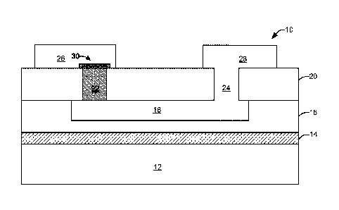
[0009] FIG. 1 illustrates cross-sectional view of a superconducting device
interconnect structure.
3
CA 03034812 2019-02-22
WO 2018/089061 PCT/US2017/045355
[0010] FIG. 2 illustrates a schematic cross-sectional view of an example
of a
superconductor structure in its early stages of fabrication.
[0011] FIG. 3 illustrates a schematic cross-sectional view of the
structure of
FIG. 2 after a photoresist material layer has been deposited and patterned,
and while
undergoing an etch process.
[0012] FIG. 4 illustrates a schematic cross-sectional view of the
structure of
FIG. 3 after the etch process and after the photoresist material layer has
been stripped.
[0013] FIG. 5 illustrates a schematic cross-sectional view of the
structure of
FIG. 4 after a contact material fill.
[0014] FIG. 6 illustrates a schematic cross-sectional view of the
structure of
FIG. 5 after undergoing a chemical mechanical polish.
[0015] FIG. 7 illustrates a schematic cross-sectional view of the
structure of
FIG. 6 after deposition of a second high temperature dielectric, a photoresist
material
layer deposition and patterning, and while undergoing an etch process to form
a first
via.
[0016] FIG. 8 illustrates a schematic cross-sectional view of the
structure of
FIG. 7 after the etch process and after the photoresist material layer has
been stripped.
[0017] FIG. 9 illustrates a schematic cross-sectional view of the
structure of
FIG. 8 after a contact material fill to form a first contact and after a
chemical mechanical
polish.
[0018] FIG. 10 illustrates a schematic cross-sectional view of the
structure of
FIG. 9 after undergoing an oxidation to form an layer on a top surface of the
first contact
and after undergoing a deoposition process to form a cap layer.
[0019] FIG. 11 illustrates a schematic cross-sectional view of the
structure of
FIG. 10 after a photoresist material layer has been deposited and patterned,
and while
undergoing an etch process.
4
CA 03034812 2019-02-22
WO 2018/089061 PCT/US2017/045355
[0020] FIG. 12 illustrates a schematic cross-sectional view of the
structure of
FIG. 11 after the etch process and after the photoresist material layer has
been
stripped.
[0021] FIG. 13 illustrates a schematic cross-sectional view of the
structure of
FIG. 12 after deposition of a low temperature dielectric, a photoresist
material layer
deposition and patterning, and while undergoing an etch process to form a
second via.
[0022] FIG. 14 illustrates a schematic cross-sectional view of the
structure of
FIG. 13 after the etch process and after the photoresist material layer has
been
stripped.
[0023] FIG. 15 illustrates a schematic cross-sectional view of the
structure of
FIG. 14 after a photoresist material layer has been deposited and patterned,
and while
undergoing an etch process to form trenches.
[0024] FIG. 16 illustrates a schematic cross-sectional view of the
structure of
FIG. 15 after the etch process and after the photoresist material layer has
been
stripped.
[0025] FIG. 17 illustrates a schematic cross-sectional view of the
structure of
FIG. 16 after a contact material fill.
[0026] FIG. 18 illustrates a schematic cross-sectional view of the
structure of
FIG. 17 after undergoing a chemical mechanical polish, and while undergoing an
etch
process to remove the low temperature dielectric layer.
[0027] FIG. 19 illustrates a schematic cross-sectional view of the
structure of
FIG. 18 after undergoing an etch process to remove the low temperature
dielectric
layer.
DETAILED DESCRIPTION
[0028] The present invention is directed to a high temperature low loss
dielectric
superconductor device (e.g., Josephson junction (JJ)) interconnect structure
and a
method for forming the same. In one example, an aluminum (AL) based
CA 03034812 2019-02-22
WO 2018/089061 PCT/US2017/045355
superconducting JJ (e.g., Al/aluminum-oxide(A10x)/AI) is incorporated into a
dual
damascene process for scaling into a high density multilevel interconnect
submicron
technology. The interconnect metal used for this integration can be, for
example,
niobium (Nb). The active JJ is required to be surrounded by high temperature
dielectrics to obtain performance targets at RF frequencies. The method
incorporates a
scalable JJ process into a planarized superconducting interconnect scheme with
a high
temperature dielectric.
[0029] A high temperature dielectric is formed of a dielectric material
that is
formed at temperatures greater than 180 C. Temperatures at greater than 180 C
can
cause damage to the structure of the JJ, while a low temperature dielectric is
formed at
temperatures that are less than 180 C which do not typically cause damage to
the
structure of the JJ. High temperature dielectrics provide superconducting
devices that
have less signal loss than devices embedded in low temperature dielectrics and
allow
for devices within the dielectric to operate with improved performance
relative to devices
embedded in low temperature dielectric.
[0030] The invention also resolves the problem of making high density JJs
of 0.5um and below into a multilevel process flow to enable high levels of
interconnects.
This present formation of JJs utilizes a scaled process technology, and
specifically
utilizes the chemical mechanical polish (CMP) of Al followed by oxidation of
the
aluminum to form the thin tunnel barrier. There is no documented evidence of a
JJ
formed on a polished surface to date when fabricating high density functional
Al/A10x/AI
JJ devices (0.35um and larger) and circuits with niobium based interconnect of
0.25um
dimensions. The aluminum based JJ has significantly different performance
characteristics compared to the common niobium based JJs.
[0031] FIG. 1 illustrates cross-sectional view of a superconducting device
JJ
interconnect structure 10. The superconducting device structure 10 includes an
active
layer 14 overlying a substrate 12. The substrate 12 can be formed of silicon,
glass or
other substrate material. The active layer 14 can be a ground layer or a
device layer. A
6
CA 03034812 2019-02-22
WO 2018/089061 PCT/US2017/045355
first high temperature dielectric layer 16 overlies the active layer 14, and a
second high
temperature dielectric layer 20 overlies the first high temperature dielectric
layer 16.
Both the first and the second high temperature dielectric layers are formed of
a
dielectric material that can be employed in high temperatures (e.g., greater
than or
equal to 180 degrees Celsius) typically utilized in the formation of
semiconductors.
[0032] A base electrode 18 is embedded in the first high temperature
dielectric
layer 16. A JJ 30 is overlays the second high temperature dielectric layer 20.
The
JJ 30 is formed from an aluminum layer with an oxidized top surface and capped
with
an aluminum layer that encapsulates the oxidized top surface. A first
conductive
contact 22 formed from, for example aluminum, extends from the JJ 26 to a
first end of
the base electrode 18 through the second high temperature dielectric layer 20.
Importantly, the first conductive contact 22 defines the width of the JJ 30.
In this
manner, the JJ can be made with a width as small as the ability of the
technology used
to make the first conductive contact 22, which is much smaller for the high
temperature
dielectric material as opposed to a low temperature dielectric material.
[0033] A second conductive contact 24 formed from, for example, niobium,
extends from the top surface of the second high temperature dielectric layer
20 to a
second end of the base electrode 18. A first side of the JJ 30 is connected to
a first
conductive line 26, which is considered the top electrode of the JJ 30. A
second
conductive line 28 is considered the counter electrode and is coupled to the
base
electrode 18 by the second conductive contact 24. The base electrode 18 is
coupled to
the second side of the JJ 30 and the counter electrode. The conductive lines
26 and 28
are formed of a superconducting material, such as niobium.
[0034] Turning now to FIGS. 2-10, fabrication is discussed in connection
with
formation of interconnects in the superconducting device of FIG. 1. It is to
be
appreciated that the present example is discussed with respect to a process
flow that
starts with the formation of either a single or dual damascene layer of
superconducting
metal in an insulating dielectric. If the JJ is formed first then it would be
a single
7
CA 03034812 2019-02-22
WO 2018/089061 PCT/US2017/045355
damascene as depicted below or dual damascene if inserted within a multi-level
interconnect. The present example will be illustrated with respect to a single
damascene trench etched into a dielectric thin film to form a bottom electrode
followed
by a dual damascene process to form a top electrode.
[0035] FIG. 2 illustrates a superconductor structure 50 in its early
stages of
fabrication. The superconductor structure 50 includes an active layer 54, such
as a
ground layer or device layer, that overlays an underlying substrate 52. The
underlying
substrate 52 can be, for example, a silicon or glass wafer that provides
mechanical
support for the active layer 54 and subsequent overlying layers. A first high
temperature dielectric layer 56 is formed over the active layer 54. Any
suitable
technique for forming the first high temperature dielectric layer 56 may be
employed
such as Low Pressure Chemical Vapor Deposition (LPCVD), Plasma Enhanced
Chemical Vapor Deposition (PECVD), High Density Chemical Plasma Vapor
Deposition
(HDPCVD), sputtering or spin on techniques to a thickness suitable for
providing an
interconnect layer. Alternatively, the first high temperature dielectric layer
56 can be
formed directly on the substrate 50.
[0036] Next, as illustrated in FIG. 3, a photoresist material layer 58 is
applied to
cover the structure and is then patterned and developed to expose a trench
opening 60
in the photoresist material layer 58 in accordance with a trench pattern. The
photoresist
material layer 58 can have a thickness that varies in correspondence with the
wavelength of radiation used to pattern the photoresist material layer 58. The
photoresist material layer 58 may be formed over the first high temperature
dielectric
layer 56 via spin-coating or spin casting deposition techniques, selectively
irradiated
(e.g., via deep ultraviolet (DUV) irradiation) and developed to form the
trench
opening 60.
[0037] FIG. 3 also illustrates performing of an etch 110 (e.g.,
anisotropic reactive
ion etching (RIE)) on the first high temperature dielectric layer 56 to form
an extended
trench openings 62 (FIG. 4) in the first high temperature dielectric layer 56
based on the
8
CA 03034812 2019-02-22
WO 2018/089061 PCT/US2017/045355
trench pattern in the photoresist material layer 58. The etch step 110 can be
a dry etch
and employ an etchant which selectively etches the underlying first high
temperature
dielectric layer 56 at a faster rate than the underlying active layer 54 and
the overlying
photoresist material layer 58. For example, the first high temperature
dielectric layer 56
may be anisotropically etched with a plasma gas(es), herein carbon
tetrafloride (CF4)
containing fluorine ions, in a commercially available etcher, such as a
parallel plate RIE
apparatus or, alternatively, an electron cyclotron resonance (ECR) plasma
reactor to
replicate the mask pattern of the photoresist material layer 58 to thereby
create the
extended trench opening 62. The photoresist material layer 58 is thereafter
stripped
(e.g., ashing in an 02 plasma) so as to result in the structure shown in FIG.
4.
[0038] Next, the structure undergoes a contact material fill to deposit a
superconducting material 64, such as niobium or tantalum (Ta) or some other
superconducting material, into the trench 62 to form the resultant structure
of FIG. 5.
The contact material fill can be deposited employing a standard contact
material
deposition. Following deposition of the contact material fill, the
superconducting
material 64 is polished via chemical mechanical polishing (CMP) down to the
surface
level of the first high temperature dielectric layer 56 to form the base
electrode 66 and
provide the resultant structure of FIG. 6.
[0039] Next, as represented in FIG. 7, a second high temperature
dielectric
layer 68 is formed over the structure of FIG. 6. The second high temperature
dielectric
layer 68 can be formed in the same manner and techniques as the first high
temperature dielectric layer 56. As shown in FIG. 7, a photoresist material
layer 70 is
applied to cover the structure and is then patterned (e.g., DUV imaged) and
developed
to expose an open region 72 in the photoresist material layer 70 in accordance
with a
via pattern. FIG. 7 also illustrates performing of an etch 120 on the second
high
temperature dielectric layer 68 to form an extended via opening 74 (FIG. 8) in
the
second high temperature dielectric layer 68 based on the via pattern in the
photoresist
material layer 70. The first extended open region 72 or via extends to the
base
9
CA 03034812 2019-02-22
WO 2018/089061 PCT/US2017/045355
electrode 66. The photoresist material layer 70 is thereafter stripped (e.g.,
ashing in an
02 plasma) so as to result in the structure shown in FIG. 8.
[0040] Next, a sputter pre-clean is performed to remove any oxidation on
the
contact material of the base electrode of FIG. 8. Furthermore, the structure
of FIG. 8
undergoes a sputter deposition of, for example, aluminum to fill the first
extended open
region 72 or via that extends to the base electrode 66 to form a conductive
contact 76.
The top surface of the first conductive contact 76 is then polished using CMP
to form a
smooth surface for forming of the JJ on top of the first conductive contact 76
to provide
the resultant structure of FIG. 9. The roughness of the polished surface is
very
important to ensure good JJ characteristics. Additionally, the width of the JJ
is defined
based on the width of the first extended open region 72 or via, and ultimately
the width
of the conductive contact 76.
[0041] Next, the top surface of the first conductive contact 76 is
oxidized to form
an oxidized top surface 79 and capped with an aluminum layer 80 to form a JJ
84
(FIG. 12). The thin oxidized aluminum 79 forms the tunnel barrier and the
aluminum
layers 78 and 80 on both sides sets the gap voltage of the JJ 84. As
illustrated in
FIG. 11, a photoresist material layer 82 is applied to cover a portion of the
structure that
defines the JJ and is then patterned and developed to remove the cap layer 80
everywhere except where the JJ is going to be formed. The photoresist material
layer 82 overlaps the thin oxidized aluminum at both ends.
[0042] FIG. 11 illustrates performing of an etch 130 (e.g., anisotropic
reactive ion
etching (RIE)) on the cap layer 80 to form the JJ 84 (FIG. 12) to define the
final JJ size.
The remaining cap layer after the etch 130 encapsulates the thin oxidized
aluminum 79.
The etch step 130 can be a dry etch that employs an etchant which selectively
etches
the trilayer stack layer 81 at a faster rate than the first conductive contact
76, the
second high temperature dielectric layer 68 and the overlying photoresist
material
layer 82. A chlorine based plasma etch is utilized as the etchant since it
will etch
superconducting materials, such as niobium, tantalum and aluminum. The
aluminum
CA 03034812 2019-02-22
WO 2018/089061 PCT/US2017/045355
oxide 79 is so thin that etching does not stop due to the presence of argon in
the
etching chemistry. The plasma etch is desired to not over-etch significantly
into the
underlying base electrode 66, which is benefited by the good planarity of the
underlying
structure to thereby create the JJ 84. The photoresist material layer 82 is
thereafter
stripped (e.g., ashing in an 02 plasma) so as to result in the structure shown
in FIG. 12.
[0043] Next, as represented in FIG. 13, a low temperature based dielectric
layer 86 (e.g., Tetraethyl Orthosilicate (TEOS)) is formed over the structure
of FIG. 12 to
encapsulate the JJ 84, and enable a plasma etch selectivity of a subsequent
etch to the
underlying second high temperature dielectric layer 68. The low temperature
based
dielectric is now used to protect the JJ 84 from subsequent processing due to
temperatures and etching processes. A photoresist material layer 88 is applied
to cover
the structure and is then patterned (e.g., DUV imaged) and developed to expose
an
open regions 90 in the photoresist material layer 88 in accordance with a via
pattern.
FIG. 13 also illustrates performing of an etch 140 on the low temperature
based
dielectric layer 86 to form extended via opening 92 (FIG. 14) in the low
temperature
based dielectric layer 86 and the second high temperature dielectric layer 68
based on
the via pattern in the photoresist material layer 88. The extended via opening
92
extends to a second end of the base electrode 66. The photoresist material
layer 88 is
thereafter stripped (e.g., ashing in an 02 plasma) to provide the resultant
structure of
FIG. 14.
[0044] Next, as represented in FIG. 15, a photoresist material layer 94 is
applied
to cover the structure and is then patterned and developed to expose open
trench
regions 96 in the photoresist material layer 94 in accordance with a trench
pattern.
FIG. 15 also illustrates performing of an etch 150 (e.g., anisotropic reactive
ion etching
(RIE)) on the low temperature based dielectric layer 86 to form extended
openings 96
(FIG. 16) in the low temperature based dielectric layer 86 based on the trench
pattern in
the photoresist material layer 94. The etch 150 is a selective etch that is
selective to
stop on the second high temperature dielectric layer 68. The photoresist
material
11
CA 03034812 2019-02-22
WO 2018/089061 PCT/US2017/045355
layer 94 is thereafter stripped (e.g., ashing in an 02 plasma) so as to result
in the
structure shown in FIG. 16.
[0045] Next, the structure undergoes a contact material fill to deposit
superconducting material 100, such as niobium, into the via 92 and trenches 98
to form
contact 100 and conductive lines 102 employing a standard contact material
deposition
to provide the resultant structure in FIG. 17. Following deposition of the
contact
material fill, the contact material is polished via chemical mechanical
polishing (CMP)
down to the surface level of the TEOS based dielectric layer 86 to provide the
resultant
structure in FIG. 18. Finally an oxide plasma etch 160 is performed on the
structure of
FIG. 18 to remove the low temperature based dielectric layer 86 to ensure no
high loss
dielectric is near the JJ 84.
[0046] A resultant final structure shown in FIG. 19 is provided that
includes
contacts that extend to the base electrode 66 and the JJ 84 coupled to
respective
conductive lines 102 to provide a structure similar to the structure
illustrated in FIG. 1.
The conductive lines 102 form a counter electrode coupled to the base
electrode 66
which is coupled to a first end of the JJ 84 with a top electrode coupled to a
second end
of the JJ 84.
[0047] What have been described above are examples of the invention. It
is, of
course, not possible to describe every conceivable combination of components
or
methodologies for purposes of describing the invention, but one of ordinary
skill in the
art will recognize that many further combinations and permutations of the
invention are
possible. Accordingly, the invention is intended to embrace all such
alterations,
modifications, and variations that fall within the scope of this application,
including the
appended claims.
12