Note: Descriptions are shown in the official language in which they were submitted.
CA 03036827 2019-03-13
WO 2018/053198
PCT/US2017/051658
STRUCTURES, SYSTEM AND METHOD FOR CONVERTING ELECTROMAGNETIC
RADIATION TO ELECTRICAL ENERGY USING METAMATERIALS, RECTENNAS
AND COMPENSATION STRUCTURES
[0001] The present application claims the benefit of U.S. Provisional App.
No.
62/394,679, filed September 14, 2016, which is hereby incorporated by
reference
herein in its entirety.
BACKGROUND
Field of the Invention
[0002] Embodiments of the present invention relate generally to structures
and
methods for harvesting energy from electromagnetic radiation. More
specifically,
embodiments relate to systems for harvesting energy from, for example, the
infrared
and near infrared (such as heat) and visible spectrums and capturing terahertz
energy.
Background of the Invention
[0003] There is a great need for inexpensive renewable energy in the world.
Ironically, there is an abundance of energy available in the form of sunlight
and heat.
Using such energy to support modern living, however, requires that energy be
converted into electrical form. In fact, most electrical energy used today
comes from
a conversion process involving heat. For example, nuclear, coal, diesel, and
natural
gas powered electrical generation plants all convert naturally stored forms of
energy
into electricity. Unfortunately, the conversion processes used in these plants
are
inefficient, and often produce more heat as waste than is converted into
electricity.
[0004] In addition to higher efficiency, harvesting sources of heat into
usable
electrical power is especially desirable at low cost. Conventional turbine-
based
solutions for generating electricity from heat are expensive. However, such
systems
have been employed for years, and are now mature. As a result, new
technological
1
CA 03036827 2019-03-13
WO 2018/053198
PCT/US2017/051658
solutions to convert heat to electrical power must provide sufficient
improvement to
overcome the status quo of turbine-based systems. Despite the maturity of
turbine-
based systems, high cost and greater demand for electricity make new
technologies
that convert heat to electricity more efficiently and at lower cost
increasingly
attractive. Among the new technologies being studied are thermo photovoltaic
(TPV), thermoelectric (TE) and at lower temperatures organic rankine cycle
(ORC).
[0005] TPV technology faces a number of hurdles in converting heat to
electricity.
Chief among them is that photovoltaic techniques convert short wave radiation
to
electricity, not the comparatively long waves of the IR and near-IR spectra
associated
with heat. New micron gap methods to bring this long wave energy to the
operating
regions of a PV cell still require conversion technology better suited to the
influx of
long wave radiation and thus are suitable only at the highest temperature
sources.
[0006] In general, the PV cell band gap favors only energetic photons since
lower
energy photons do not have the energy to cross the gap. As a result, these
lower
energy photons are absorbed by the PV cell, and cause heat in the cell itself
[0007] Thermoelectric (TE) solutions, to date, have only been able to
convert heat to
electrical power at low efficiency. As a result, conventional TE solutions
have not
provided substantial efficiencies in energy conversion. Even so, TE has found
application in automotive waste heat recovery, which further evidences the
need for
alternative heat-to-electric conversion technologies.
[0008] Organic Rankine Cycle (ORC) and related technologies harvest waste
heat by
chaining turbines together with each successive system in the chain using a
lower
boiling point liquid. ORC system have a number of drawbacks. They are bulky,
have
large numbers of moving parts, contain chemicals that are undesirable on
customer
sites and are limited to the properties of the liquids in the system.
Ultimately, they
2
CA 03036827 2019-03-13
WO 2018/053198
PCT/US2017/051658
suffer from limits of conversion time, space, and the diminishing returns of
additional
systems in a working space.
[0009] These and other problems with conventional techniques for harvesting
electrical energy from heat require a solution with greater efficiency and
lower costs.
BRIEF SUMMARY OF THE INVENTION
[0010] In an embodiment, a system for harvesting electrical energy from
electromagnetic (EM) radiation emitted by a hot source comprises a nanoantenna
electromagnetic collector (NEC) film of collector/converter devices (called
rectennas)
that collect heat radiation emanating from a heat source, and converts that
heat
radiation to electrical energy.
According to embodiments include rectennas
comprising an antenna tuned to resonate in the presence of frequencies
associated
with heat, and a diode to rectify the single produced by the antenna in the
presence of
heat. The rectennas can be combined in various embodiments with one or more
of:
(1) a three dimensional (3D) metamaterial to frequency shift and compress,
concentrate and make coherent the electromagnetic field; (2) THz compensation
circuitry using transmission line structures to address antenna and diode
impedance
matching as well as created diode capacitance; and (3) metal-insulator-metal
(MIM)
or metal-insulator-insulator-metal (MIIM) diodes using Cobalt and its oxides
with
other metals such as Titanium and its oxides. The
electricity generated by the
rectennas in the NEC film can combined and supplied to a load for commercial
purposes.
[0011] In an embodiment, a 3D metamaterial is designed to concentrate an EM
field
created by heat on the surface of the metamaterial. NEC devices (rectennas)
are
positioned in the near field directly over patterned holes (or poles) in the
metamaterial
overcoat of the hot body. In an embodiment, a hot gas is encased in metal as
in a flue
3
CA 03036827 2019-03-13
WO 2018/053198
PCT/US2017/051658
for instance. The metal casing then is the hot side material. A NEC film is
then
attached, metamaterial side first. Preferably, the metamaterial does not
contact the
rectenna. This leaves an air gap or vacuum to separate the metamaterial for
reduction
of heat conduction. A reflective layer is constructed and added at an offset
distance.
The offset distance can be calculated by simulation of the optical properties
exhibited
by the materials and structures at a desired frequency of NEC operation.
[0012] In an embodiment of the invention, the NEC device is a rectenna
using metal-
insulator-insulator-metal (MIIM) diodes constructed with Co-CoOx and TiOx-Ti
although other single or double insulator diodes with equal or better
performance may
be used.
[0013] In an embodiment of the invention, impedance matching between the
antenna
elements of the NEC and the diode may be performed using a single- or multi-
node
tank circuit that trades current for voltage. Trading current for voltage
supplies a
boosted voltage to the diode. The tank circuits also matches the impedance of
the
rectenna antenna to a higher impedance MIM/MIIM diode. In embodiments, a
compensation circuit may also be used to reduce the effects of diode
capacitance. In
an embodiment, the compensation circuit uses the capacitance of the MIM/MIIM
device itself as part of the compensation structure. Given the very high
frequency of
these devices, the tank circuit and compensation structures are constructed
using
transmission line elements that act as either capacitors or inductors. The
transmission
line elements are designed using simulations of 3D EM waves in materials and
structures.
[0014] The basic rectenna circuit is relatively well understood. A rectenna
circuit
comprises an antenna that, depending on the strength of the source, produces a
small
voltage (-1mV or less) at a high frequency (> 1THz) across a MIM or MIIM
diode.
4
CA 03036827 2019-03-13
WO 2018/053198
PCT/US2017/051658
Because naturally occurring sources of THz are very low power, antennas will
supply
far lower output voltages in those cases. In the THz range, existing
semiconductor
diodes cannot replenish charge carriers fast enough to keep up, that is, track
the wave
of voltage or current. When these oscillate too fast, the device fails to
"keep up" and
fails to perform its operation. . Metal-insulator-Metal diodes perform well
within the
THz range since, unlike the materials used in semiconductor diodes, the metals
that
comprise them are not charge carrier limited.
[0015] Using conventional rectennas, efficient conversion of natural THz
sources is
low for several reasons. The nonlinearity of the rectenna's diode's current-
voltage
characteristic curve occurs at a significantly higher voltage (-100mV) than
the
voltage output of the rectenna's antenna (-1mV or less). While the voltage
location
of the knee of the diode nonlinearity can be reduced, such reduction is
limited by
properties of the materials of the diode's elements and the ease of
manufacture of the
diode's elements. For instance, a MIM/MIIM diode operates by tunneling of
electrons from one metal to another through the barrier of the insulator(s)
separating
them. The height of this barrier has a relationship to the resistance and
effectiveness
of tunneling of the diode. The height of a barrier is the difference of the
electron
affinity of the insulator(s) and the work function of the adjacent metal.
Additional
insulators can create asymmetry. Selection of metals with differing work
functions
may also add to asymmetry. Low barriers and high asymmetry are desirable since
they allow low voltage tunneling.
[0016] A metric often used in diode design is responsivity. Responsivity is
the ratio
of the second derivative of the diode's current/voltage curve over the first
derivative,
and is measured in Amps/Watt. High responsivity is desirable and given the low
CA 03036827 2019-03-13
WO 2018/053198
PCT/US2017/051658
voltage environment of rectennas in energy harvesting, a diode's responsivity
value
around zero (0) volts bias of the diode is a key metric.
[0017] Embodiments of the present invention implement a metal-insulator-
insulator-
metal (MIIM) diode with high zero bias responsivity and low resistance
suitable for
converting heat into electricity. MIIM diodes are most suited to convert heat
to
electricity over other kinds of diodes due to their high frequency (THz)
capability.
Previously disclosed MIIM diodes may have high zero bias responsivity but with
high
resistance. Low resistance in the diode enables low RC time constants, which
then
enables higher efficiency in converting heat to electricity. Suitable MIIM
devices and
fabrication methods are described in further detail herein.
[0018] Another important aspect of embodiments of the present invention is
thermal
management. It is important to supply a heat differential to just the
collector/converter devices, and not allow the heat source to become generally
cooled.
To optimize heat transfer from the heat source to the collector/converter
device, an
embodiment of the present invention includes an optimization layer that allows
cooling of the converter elements of the collector/converter devices while
insulating
the other areas of the surface.
[0019] In an embodiment, the optimization layer is an overcoat of two
materials - one
that is highly insulating and another that is highly conducting of heat.
Insulating
materials or vacuum are placed so as to block heat flow to regions of the NEC
film
that do not contain collector/converter devices. Heat conducting materials are
placed
so as to allow heat flow to the collector/converter devices.
[0020] Embodiments include an additional improvement to the rectenna
circuit,
termed "compensation circuitry." Compensation circuits comprise passive
circuit
elements, such as capacitors and inductors. These elements are combined to
provide a
6
CA 03036827 2019-03-13
WO 2018/053198
PCT/US2017/051658
voltage boost and impedance match between the antenna and the diode. The
general
design is sometimes referred to as a tank circuit. Several embodiments of such
compensation circuits are disclosed. For instance, single- and multi-tank
compensation circuits are disclosed. An embodiment of a compensation circuit
that
uses the rectenna diode as the capacitor for the circuit is also disclosed.
[0021] An advantage of compensation circuits as disclosed herein is the
tradeoff of
antenna current for voltage. This is particularly useful because supplying a
higher
voltage to the diode places it in a better operating point along its current-
voltage
characteristic. Moreover, this tradeoff matches the low impedance of the
antenna
(about 100 ohms) to the higher impedance diode.
[0022] Another advantage of compensation circuits as disclosed herein is in
smoothing out the shape of the voltage and current in the circuit.
Compensation
circuits as disclosed herein make the voltage and current curves conform to a
more
sinusoidal shape for more efficient power harvesting.
[0023] A second embodiment of a compensation circuit addresses the inherent
capacitance of the diode. This compensation circuit is comprised of an
inductor and a
capacitor in parallel with the diode. Placing inductance in parallel with a
capacitance
cancels the imaginary component of the capacitance. As such, when properly
designed this compensation circuit can solve the long RC time constant problem
that
has been associated with MIM and MIIM diodes.
[0024] At THz frequencies, conventional inductors (coils) cannot be used.
As such,
in embodiments, capacitors and inductors are created in the compensation
circuits
through "transmission lines" designed to appropriate dimensions. Transmission
lines
have unique properties of being able to exhibit either capacitance or
inductance
depending on their length relative to the length of the waves in the line.
7
CA 03036827 2019-03-13
WO 2018/053198
PCT/US2017/051658
[0025] An important design criteria for many components of embodiments is
the
uniformly small bandwidth of the energy and electronic circuits. Conversion of
black
body radiation to electricity is generally viewed as a wide bandwidth problem
because
the Boltzman curve extends from single digit THz into the hundreds of THz.
Reducing this bandwidth according to embodiments begins with the use of a
metamaterial to form a plasmon resonance. This plasmon resonance is designed
in
combination with the rectenna antenna's slightly greater bandwidth to maximize
energy transfer into the rectenna. The antenna then supplies a relatively
narrow band
signal to the compensation circuit elements. This is important since the
compensation
circuits only work well in resonant bands. These bands are designed to match
the
incoming band from the rectenna's antenna. In this way elements of the system
work
together for efficient harvesting.
[0026] In an embodiment, the resonant elements of the collector/converter
devices
comprise electrically conductive material coupled with a transfer structure
(diode) to
convert electrical energy stimulated in the resonant element to direct
current.
Exemplary such resonant elements are described in more detail in U.S. Patent
Nos.
7,792,644, filed November 13, 2007, entitled, "Methods, computer readable
media,
and graphical user interfaces for analysis of frequency selective surfaces"
and
6,534,784, filed May 21, 2001, entitled, "Metal-oxide electron tunneling
device for
solar energy conversion", and U.S. Patent App. Nos. 11/939,342, filed November
13,
2007, entitled, "Structures, Systems and Methods for Harvesting Energy from
Electromagnetic Radiation" (U.S. Patent Pub. No. 2010/0284086), and 11/471223,
filed June 20, 2006, entitled, "Systems and methods for roll-to-roll
patterning" (U.S.
Patent App. Pub. No. 2006/0283539) each of which is incorporated by reference
herein in its entirety.
8
CA 03036827 2019-03-13
WO 2018/053198
PCT/US2017/051658
[0027] Additional features and embodiments of the present invention will be
evident
in view of the following drawings and detailed description of the invention.
BRIEF DESCRIPTION OF THE DRAWINGS
[0028] Fig. 1 is a schematic diagram of a system for harvesting energy from
a heat
source and supplying the generated electricity to a load.
[0029] FIG. 2 is an orthographic projection of a metamaterial and coupled
rectenna
with associated compensation circuitry according to an embodiment of the
present
invention.
[0030] FIG. 3 is a cross-section view of an exemplary metamaterial
structure
illustrating a 3D confinement of plasmonic energy and resulting concentration
of e-
field at a region where the antenna is positioned according to an embodiment
of the
present invention.
[0031] FIG. 4 is a cross section of metamaterial coupled rectenna showing
an
exemplary antenna, metamaterial substrate, and that illustrates an engineered
placement of rectenna between a lower metamaterial and a reflector structure
according to an embodiment of the present invention.
[0032] FIG. 5 is a schematic illustration of a compensation structure
arranged at the
feed point of an antenna element for the purpose of performing impedance
matching
between antenna and diode.
[0033] FIG. 6 is a cutaway drawing that illustrates an embodiment of using
microstrip
transmission lines with engineered geometry and permittivity of surrounding
materials to achieve THz transportation of energy and tuning of impedance.
[0034] FIG. 7 is a schematic diagram of an equivalent Rectenna circuit
illustrating
that the nonlinear reactance of the antenna and nonlinear reactance of the
diode can be
compensated for with an impedance matching network and a resistive load.
9
CA 03036827 2019-03-13
WO 2018/053198
PCT/US2017/051658
[0035] FIG. 8 illustrates a top-view of an antenna structure and antenna
geometric
parameters that can be tailored for maximum plasmonic energy transfer to the
antenna
feed point and to the attached transmission line structure according to an
embodiment
of the present invention.
[0036] FIG. 9 illustrates a further embodiment to tailor the compensation
circuitry
through tapping the antenna off-center and nonsymmetrical between arms of the
bowtie resulting in variance in the fringing fields and alteration of
impedance.
[0037] FIGs. 10A, 10B, and 10C illustrate several transmission line circuit
elements
to compensate for the high parasitic capacitance of THz diodes using elements
of
transmission line according to embodiments.
[0038] FIG. 10D further illustrates compensation of diode capacitance when
the diode
is directly embedded in the feed point of the antenna.
[0039] FIG. 11 is a technical illustration of single pole compensation
structures
perpendicular to the feed point of an antenna, with the differential
transmission line
elements in a balanced mode of operation.
[0040] FIG. 12 is a technical illustration of single pole compensation
structures
perpendicular to the feed point of an antenna, with the differential
transmission line
elements in an unbalanced mode of operation.
[0041] FIG. 12A is a chart containing stub lengths and distances for a
compensation
circuit as well as measured responses according to an embodiment of the
present
invention designed for 1THz.
[0042] FIG. 13A illustrates in cross section an exemplary MIIM structure
for diode
according to an embodiment.
[0043] FIG. 13B is a graph illustrating a responsivity vs. voltage curve of
a MIIM
diode fabricated according to an embodiment of the present invention.
CA 03036827 2019-03-13
WO 2018/053198
PCT/US2017/051658
[0044] FIG. 14 is a cutaway drawing illustrating one embodiment of
connecting a
metal-insulator-insulator-diode between a differential transmission line in a
method
that reduces parasitic reactance of the diode.
[0045] FIG. 15 is illustrates integration of a THz rectifying diode to a
differential
transmission line having a broad-band transmission line compensation structure
using
multiple stubs to achieve a multi-pole resonant response and that also serves
to boost
the voltage to the diode according to an embodiment of the present invention.
[0046] FIG. 16 illustrates a broad-band transmission line compensation
structure that
implements multi-stage stepped impedance elements to act as an impedance
transformer between the antenna and diode according to another embodiment of
the
present invention.
[0047] FIG. 17 illustrates a broad-band transmission line compensation
structure that
implements ladder topology stepped impedance transforms to replicate lumped
element L-C behavior according to another embodiment of the present invention.
[0048] FIG. 18 illustrates a fractal bowtie antenna that provides means to
engineer the
electron/plasmonic wave conduction path and the relative refractive index of
the
antenna according to an embodiment.
[0049] FIG. 19 is an orthographic projection illustrating use of a tapered
transmission
line to guide and focus surface waves to a nanofocus in the region of the
diode.
[0050] FIG. 20 illustrates a cross sectional diagram of a metamaterial with
a
metamaterial coupled rectenna that comprises a rectifying antenna (rectenna)
with a
near field metal reflector over a hole in a metamaterial according to an
embodiment.
[0051] FIG. 21 illustrates a cross sectional diagram of a metamaterial with
a
metamaterial coupled rectenna that comprises a rectifying antenna (rectenna)
with a
far field DBR reflector over a hole in a metamaterial according to an
embodiment.
11
CA 03036827 2019-03-13
WO 2018/053198
PCT/US2017/051658
[0052] FIG. 22A illustrates the electric field magnitude (V/m) of SP modes
generated
using far-field excitation of a metamaterial (patterned Copper (Cu)) surface
with no
reflector.
[0053] FIG. 22B illustrates the electric field magnitude (V/m) of SP modes
generated
using far-field excitation of a metamaterial (patterned Cu) surface that are
significantly confined in the vertical direction using a reflector.
[0054] FIG. 23 illustrates a cross section of 3D metamaterial with a
metamaterial
coupled rectenna.
[0055] FIG. 24A illustrates a rectenna during fabrication to show vias
etched or
ablated through the substrate.
[0056] FIG. 24B illustrates a rectenna during fabrication after metal
deposition of the
eventual backside contacts by filling the vias with a conductive material.
[0057] FIG. 24C illustrates a rectenna during fabrication illustrating
after formation
of distinct interconnects on the backside of the substrate.
[0058] FIG. 24D illustrates a rectenna 208 with a reflector 402 that also
serves as a
local interconnect, combined with global interconnects on the backside of the
substrate (side view).
[0059] FIG. 24E illustrates a top down view of a group of 8 rectifying
antennas that
are locally connected in series by two reflector/local interconnects between
the
substrate and rectifying antenna, each reflector interconnect connecting
either the p-
side or n-side of the diodes.
[0060] FIG. 25 is a schematic diagram of an equivalent circuit that
illustrates a basic
conventional rectenna circuit.
12
CA 03036827 2019-03-13
WO 2018/053198
PCT/US2017/051658
[0061] FIG. 26 is a schematic diagram of an equivalent circuit that
illustrates a basic
two-pole resonant structure implemented with discrete components, in
accordance
with an embodiment of the present invention.
[0062] FIG. 27 is a schematic diagram of an equivalent circuit that
illustrates a higher
order four-pole resonant structure implemented with discrete components
according
to an embodiment of the present invention.
[0063] FIG. 28 is an exemplary voltage vs. current characteristic curve of
a typical
diode used in a rectenna circuit according to an embodiment of the present
invention.
[0064] FIG. 29 is a schematic diagram of an equivalent circuit that
illustrates a two-
pole compensation structure for diode capacitance implemented with discrete
components, in accordance with an embodiment of the present invention.
[0065] FIG. 30 is a schematic diagram of an equivalent circuit that
illustrates a four-
pole compensation structure for diode capacitance implemented with discrete
components, in accordance with an embodiment of the present invention.
[0066] FIG. 31 is a schematic diagram of an equivalent circuit that
illustrates a four-
pole compensation structure for diode capacitance implemented with discrete
components, in accordance with another embodiment of the present invention.
[0067] FIG. 32 is a schematic diagram of an equivalent circuit that
illustrates a
modified four-pole resonant structure implemented with discrete components, in
accordance with an embodiment of the present invention.
[0068] FIG. 33 is a schematic diagram of an equivalent circuit that
illustrates an input
impedance boost structure and diode capacitance compensation circuit
implemented
using transmission line components, in accordance with embodiments of the
present
invention.
13
CA 03036827 2019-03-13
WO 2018/053198
PCT/US2017/051658
[0069] FIG. 34 shows simulated voltage and currents corresponding to a
conventional
rectenna circuit that is without compensation circuitry described herein.
[0070] FIG. 35 shows simulated voltage and currents corresponding with the
addition
of compensation circuitry according to an embodiment of the present invention.
[0071] FIG. 36 illustrates a frequency response curve corresponding to a
compensation circuit according to an embodiment of the present invention.
DETAILED DESCRIPTION
[0072] The following description is presented to enable one of ordinary
skill in the art
to make and use the invention and is provided in the context of a patent
application
and its requirements. Various modifications to the described embodiments will
be
readily apparent to those skilled in the art and the generic principles herein
may be
applied to other embodiments. Thus, the present invention is not intended to
be
limited to the embodiments shown but is to be accorded the widest scope
consistent
with the principles and features described herein.
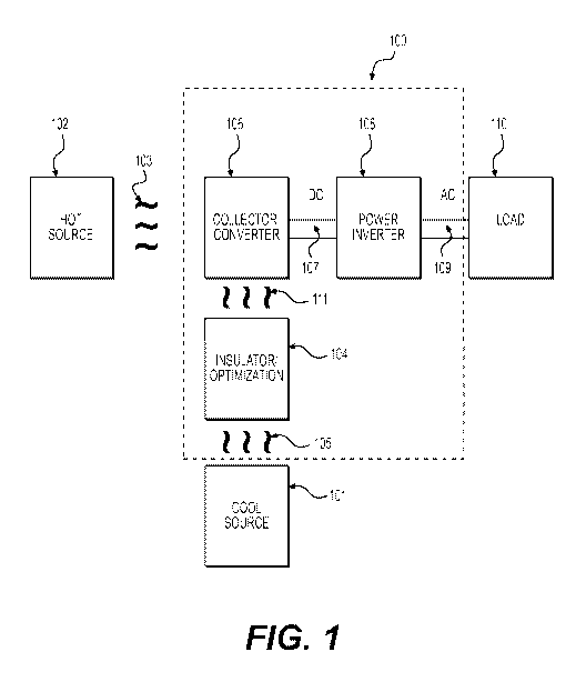
[0073] Fig. 1 is a schematic diagram of a system 100 for harvesting energy
from a
heat source 102 and supplying the generated electricity to a load 110. A
collector/converter device 106 collects heat 103 provided by heat source 102
and
converts that heat to direct current (DC). In embodiments, the DC is converted
to
alternating current (AC) by coupling collector/inverter 106 to a power
inverter 108
over a bus 107. The generated AC can then be supplied to load 110 over a bus
109.
Conversion to AC is optional as some applications may require direct DC.
[0074] In an embodiment, an insulator/optimization layer 104 is interposed
between
cool source 101 and collector/converter device 106. Insulator/optimization
layer 104
optimizes heat transfer 111 from heat source 102 to collector/converter 106 to
make
converting heat generated by heat source 102 to electricity by
collector/converter
14
CA 03036827 2019-03-13
WO 2018/053198
PCT/US2017/051658
device 106 more efficient. In an embodiment, insulator/optimization layer 104
operates by selectively allowing thermal access 105 to a cool source 101 where
needed at converter elements of collector/converter 106 and thermally
insulating
elsewhere.
[0075] In an embodiment, collector/converter 106 comprises a plurality of
collector/converter devices, for example, nanoantenna electromagnetic
collector
(NEC) devices, also called rectennas. Each NEC device comprises a resonant
structure that is tuned to heat frequencies or to the surface plasmon resonant
frequencies of a paired metamaterial, and generates an electric current in the
presence
of electromagnetic energy from heat sources. In an embodiment, a transfer
structure
converts electrical energy stimulated in the resonant elements of the NEC's
resonant
structure to DC. In an embodiment, the transfer structure is a metal insulator
metal
(MIM) or a metal-insulator-insulator-metal (MIIM) diode. In an embodiment,
collector/converter 106 comprises a film that contains a high density of NEC
devices
that cover the surface of the film. A film so constructed is referred to as a
NEC film.
[0076] Additional details concerning NEC devices and metamaterials as
described
herein can be found in U.S. Patent Application Nos. 14/745,299, filed June 19,
2015
(US 2015-0335962), 14/187,175, filed February 21, 2014 (US 20140126441),
14/108,138, filed December 16, 2013 (US 20140172374), and 13/708,481, filed
December 7, 2012 (US 20130146117), each of which is hereby incorporated herein
by
reference in its entirety.
3D Metamaterial Coupled Rectenna
System Level Description
[0077] FIG. 2 is an orthographic projection of a metamaterial 200 and
coupled
rectenna 206 with associated compensation circuitry 205 according to an
embodiment
CA 03036827 2019-03-13
WO 2018/053198
PCT/US2017/051658
of the present invention. Together metamaterial and coupled rectenna 206 are
referred to herein as a metamaterial coupled rectenna 208. As illustrated in
FIG. 2,
metamaterial coupled antenna 208 comprises a rectenna 206 positioned above a
metamaterial 200. Preferably metamaterial 200 is a 3D metamaterial
characterized by
a pattern of features on its surface 210. For example, in embodiments, the
features
can be holes or poles. As illustrated in FIG. 2, for example, 3D metamaterial
200 is
designed with sub-wavelength holes/features 201. Holes 201 induce and channel
plasmonic waves on the surface of metamaterial 200 as well as concentrate
electromagnetic e-fields at a specific bandwidth and frequencies of operation.
A
rectenna 206 includes an antenna element 202. In an embodiment, rectenna is
positioned above hole 201.
[0078] Metamaterial and coupled rectenna 206 also includes transmission
line 205
that comprises transmission line leads 205a and 205b. Transmission line 205
couples
a voltage signal generated by antenna element 202 to a diode 210. Diode 210
operates to rectify the voltage signal to generate a DC current. Together
antenna
element 202 and diode 210 comprise rectenna 206.
[0079] FIG. 3 is a cross-section view of an exemplary metamaterial
structure
illustrating a 3D confinement of plasmonic energy and resulting concentration
of e-
field 302 at a region where antenna element 202 is positioned. The
concentration of
energy is a function of the geometry of the metamaterial features and relative
positioning of antenna element 202 and upper reflector 402 (described below).
Upper
reflector 402 has a gap above the rectenna in this embodiment but other
embodiments
may use a contiguous layer or near contiguous reflector layer. Rectenna
element 206
may also be positioned at differing positions between reflector layer 402 and
the
metamaterial As illustrated in FIG. 3, in operation, antenna element 202 is
positioned
16
CA 03036827 2019-03-13
WO 2018/053198
PCT/US2017/051658
in an e-field 302 at the point of maximum intensity during operation of an
embodiment. In an embodiment, antenna element 202 is designed with a
complementary bandwidth and operating frequency for optimal coupling of energy
from the metamaterial. For example, antenna element 202 is designed to match
the
small bandwidth of the surface plasmons and tuned to the surface plasmon
resonant
frequency.
[0080] FIG. 4 is a cross section of metamaterial coupled rectenna 208 in
FIG. 2 taken
at A-A' showing an exemplary antenna, metamaterial substrate, and that
illustrates an
engineered placement of rectenna 206 between lower metamaterial 200 and
reflector
structure 402 according to an embodiment of the present invention. FIG. 4
illustrates
rectenna 206 (including antenna element 202) suspended above metamaterial hole
201
and below a top metamaterial reflector 402. During fabrication of an
embodiment,
positioning of the antenna element in the Z direction is controlled by
deposition of
standoff layer(s) 404. Standoff layer(s) 404 act as an electrical and thermal
insulator
while providing low loss optical transmission that allows radiation through
standoff
layer(s) 404. A non-exhaustive list of materials having these properties
include
5i02, 5U8, aerogels. In an embodiment, standoff layer(s) 404 are a vacuum with
the
exception of standoff material above the rectenna 206 in order to hold it in
proper
location.
[0081] Referring back to FIG 2, a transmission line 205 extends from a feed
point 203
of antenna element 202. In an embodiment, transmission line 205 comprises
transmission line leads 205a and 205b. Transmission line leads 205a and 205b
act as
a wave guide to connect to a rectifier diode 210. The combination of an
antenna
element 202 with a diode 210 is termed a rectenna, such as rectenna 206. In an
embodiment, transmission line elements 205a and 205b are designed to perform
17
CA 03036827 2019-03-13
WO 2018/053198
PCT/US2017/051658
impedance matching of antenna element 202 with diode 210. Rectified DC is
taken
off the rectenna 206 antenna element 202 by leads 222a and 222b and passed to
a bus
structure (not shown). In an embodiment, the bus structure also interconnects
multiple rectenna elements together.
[0082] In an embodiment, antenna element 202 is designed to absorb
plasmonic
radiation at terahertz (THz) frequencies radiated from metamaterial 200 in the
presence of heat. In operation, antenna element 202 generates evanescent
surface
waves that propagate to the antenna feed point 203 and are channeled through
impedance matching transmission circuit 205 to diode 210. In embodiment, diode
210 is a metal-insulator-metal (MIM) diode. In embodiment, diode 210 is a
metal-
insulator-insulator-metal (MIIM) diode. Such a MIIM diode for use in
embodiments
is described in more detail with respect to Figs 13A and 28. In an embodiment,
impedance matching transmission line 205 comprises transmission line leads
205a
and 205b.
[0083] In an embodiment, 3D metamaterial 200 employs a metal-insulator-
metal
structure for field confinement and wave guidance of a generated surface
plasmons.
The structure has metallic boundaries that introduce reflections to
constructively
interfere, channel, and localize the generated surface plasmon. Referring back
to FIG.
4, metamaterial coupled rectenna 208 has a multi-layer structure. In
operation, a heat
source is applied to an underside of 404 (layer #1) via of metamaterial
coupled
rectenna 208. In an embodiment, metamaterial periodic hole features 201 are
designed in the surface of the metamaterial 200 with a geometry to tune
metamaterial
200 for plasmonic resonance at the frequency of THz energy harvesting. For
instance, at 5THz the spacing between holes could be in the range of 45um.
Hole
could be near 15um but dimensions may vary considerably depending on
materials,
18
CA 03036827 2019-03-13
WO 2018/053198
PCT/US2017/051658
effects of rectenna 206, reflector 402 distance from the metamaterial, etc.
The depth
of the hole 201 is optimized to push more light out and localize it onto
antenna
element 202 of rectenna 206. Antenna element 502 therefore acts as a photon
collector.
[0084] To fabricate metamaterial 200, a periodic pattern of holes 201 are
drilled into a
material 200 (generally a metal). The spacing or periodicity of the hole is
designed to
sustain a surface plasmonic wave and to couple energy to each antennal element
202.
In alternate embodiments, the hole pattern is aperiodic and/or holes are of
varying
sizes. In an embodiment, arrays of rectennas 206 are implemented. Referring
back to
FIG. 2, a single unit cell of a metamaterial rectenna 208 is illustrated. In
an
embodiment, this unit cell is replicated to create large area arrays of energy
harvesting
structures.
[0085] Metamaterial coupled rectenna 208 further comprises an upper
metamaterial
reflector structure 402. In an embodiment, substrate 406 and metamaterial
reflector
structure 402 are separated with inert spacer material such as standoff
layer(s) 404.
The inert spacer material provides support and positioning of rectenna 206.
Variations on this design are shown in Fig. 4 whereby the positioning of the
rectenna
and surrounding material are optimized to provide cooling of the rectenna and
insulation around the rectenna to maximize efficiency of the system.
Additional
details concerning thermal management for embodiments is described in U.S.
Patent
App. No. 14/187,175, filed February 21, 2014, entitled, "Structures, System,
and
Method for Converting Electromagnetic Radiation to Electrical Energy," U.S.
Pat.
Pub. No. 2016/0126441, which is hereby incorporated herein by reference in its
entirety.
19
CA 03036827 2019-03-13
WO 2018/053198
PCT/US2017/051658
System Level Integration of multi-stage compensation
Impedance match and Vboost
[0086] In an embodiment, antenna element 202 of rectenna 206 is a bowtie
antenna
with an antenna feed point 203. Attached to antenna feed point 203 is a
coplanar
differential transmission line 205. Differential transmission line 205 is
comprised of
differential transmission line leads 205a and 205b. Differential transmission
line
leads 205a and 205b act as a dual microstrip transmission line structure to
integrate
diode 210 into rectenna 206 for the purpose of rectification of THz signals
received
by the antenna element 202. Diode 210 can be a MIM diode, MIIM diode, or any
other diode that can rectify signals in the THz frequency range. As described
in
further detail below, transmission line 205 is designed to implement an
impedance
transform between antenna element 202 and diode 210 to achieve maximum power
transfer. Transmission line 205 also transforms antenna current into a diode
voltage
boost to ensure the diode is biased into a nonlinear operating mode.
[0087] In an embodiment, the impedance matching circuit provided by
transmission
line 205 operates to match the complex impedance of antenna element 202 to the
complex impedance of diode 210, for example a high resistance MIM or MIIM
diode.
An exemplary such high resistance MIIM diode 210 is illustrated in FIGs. 15A
and
15B. The impedance matching network is based on lumped passive elements (e.g.,
inductors and capacitors) as shown, for example, in the equivalent circuit
schematic
diagrams illustrated in FIGs. 26-27 and 29-33 as explained in more detail
below. In
an embodiment, rather than use discrete component capacitor and inductors, the
impedance matching network in is implemented using high frequency distributed
elements (e.g., transmission lines and stubs) that act as discrete capacitor
and inductor
elements at high, e.g. THz, frequencies.
CA 03036827 2019-03-13
WO 2018/053198
PCT/US2017/051658
[0088] FIG. 5 is a schematic illustration of a compensation structure 500
arranged at
feed point 203 of antenna element 202 for the purpose of performing impedance
matching and voltage boost between antenna and diode. As shown in FIG. 5,
according to an embodiment, compensation structure 500 comprises transmission
line
205 that comprises structures comprised of differential, co-planar
transmission line
elements or leads 205a and 205b, and stubs 501a-d. Compensation structure 500
also
boosts the voltage to the diode and introduces inductive reactance to cancel
out diode
capacitance. In an embodiment, and at a representative frequency of 1THz, the
compensation structure illustrate in FIG. 5 is a quarter wavelength
transformer 500
implemented via transmission line 205 according to an embodiment. Quarter
wavelength transformer 500 includes open stubs 501a, 501b, 502a, and 502b. In
an
embodiment, stubs 501a, 501b, 502a, and 502b are interconnected to perform
quarter-
wave transformers for impedance matching of antenna to diode. Stubs 501a and
501b
are positioned at a distance 512 from feed point 203. In an embodiment,
distance 512
is 4p.m. Stubs 502a and 502b are positioned at a distance 514 from feed point
203. In
an embodiment, distance 514 is 9p.m. Diode 210 is placed at a distance 516
from feed
point 203. In an embodiment, distance 516 is 12p,m.
[0089] As described in more detail below, at high, such as THz frequencies,
open
stubs 501a, 501b, 502a, and 502b implement L-C network behavior that performs
impedance matching between antenna element 202 and diode 210, as well as
provides
a voltage boost to raise the signal to be converted by diode 210 closer to, if
not in the
optimal operating range of diode 210. The impedance transformer is a function
of the
spacing between stubs 501a and 501b and between stubs 502a and 502b, as well
as
their respective lengths. Diode 210 also introduces parasitic capacitance from
the
metal-insulator-metal interface. In an embodiment, diode 210 is placed a
distance
21
CA 03036827 2019-03-13
WO 2018/053198
PCT/US2017/051658
518 to compensate for this parasitic capacitance by transmission line segments
504a
and 504b. In an embodiment, distance 518 is 4 p.m from the end of a
transmission
line 205.
[0090] The output of antenna element 202 is input to a differential
impedance
matching network, such a quarter wavelength transformer 500, through feed
point
503. The differential impedance matching network comprises a transmission line
205. In one embodiment transmission line 205 is implemented using differential
micro strips 205a and 205b.
[0091] FIG. 6 is a cutaway drawing that illustrates an embodiment of using
microstrip
transmission lines with engineered geometry and permittivity of surrounding
materials to achieve THz transportation of energy and tuning of impedance.
FIG. 6
also illustrates that the phase of the EM radiation can be tailored using an
embodiment. As illustrated in FIG. 6, in an embodiment, microstrip
transmission
lines 205a and 205b comprise a conductive strip of width "Wl" and "W2" and
thickness "t". Widths W1 and W2 are preferably the same, but need not be.
Transmission line leads 205a and 205b are separated by a dielectric layer
(a.k.a. the
"substrate") of thickness "H" from a wider ground plane 602. Microstrip
transmission
lines 205a and 205b channel specific wavelengths of electric field lines. In
theory,
half of the EM field lines are contained within the substrate below and the
other half
within the material above. Thus, the effective permittivity (Jeff) is taken to
be the
average of the two. In operation, the transport of energy can be tuned by
selecting
specific materials with different permittivity. Other variable dimensions that
can be
adjusted are: signal (S), gap widths (w), substrate height (h) and substrate
permittivity
(Er). Decreasing "S" width increases characteristic impedance. Combinations of
all
22
CA 03036827 2019-03-13
WO 2018/053198
PCT/US2017/051658
parameters control antenna radiation coupling efficiency (accepted power),
real and
imagery impedance, and resonance.
[0092] The baseline design selects transmission lines with a specific
electrical length
(or phase length). In an embodiment, this length is in terms of the phase
shift
introduced by transmission over that conductor at some frequency. The number
of
wavelengths, or phase, involved in a wave's transit over a segment of
transmission
line is tailored via repetitive simulations whose results are plotted and
compared to
show best results. The electrical length of a transmission line is primarily
dependent
on two factors: 1) the velocity factor of the line and 2) the frequency of
operation.
[0093] Tuning Velocity of Propagation. The propagation delay is the length
of time it
takes for a signal to travel down a conductor to its destination. In a
transmission line,
a signal travels at a rate controlled by the effective capacitance and
inductance per
unit of length of the transmission line. Stubs and shorts alter the reactance.
The
velocity of propagation, that is, the speed at which a wavefront of an
electromagnetic
signal passes through the medium relative to the speed of light, is tuned by
tailoring
the metal conductivity of transmission line leads 205a and 205b and the
permittivity
of the standoff layer insulator 404 as shown in FIG. 4. Materials are selected
to
optimize simulation results.
Transmission Line Stubs
[0094] A primary building block of compensation circuits according to
embodiments
are stubs 501a-b and 502a-b connected to a transmission line leads 505a and
505b. A
stub is a length of transmission line that is connected at one end only. It is
terminated
in a short (or open) circuit. The length of the stub is chosen to produce the
desired
impedance. The input impedance of the stub is purely reactive, either
capacitive or
inductive. Stubs work by means of standing waves along their length. Their
reactive
23
CA 03036827 2019-03-13
WO 2018/053198
PCT/US2017/051658
properties are determined by their physical length in relation to the
wavelength of the
standing EM wave along their length. Thus, stubs may function as capacitors or
inductors. Full wave finite element analysis of the metamaterial coupled
rectenna
structure 208 is performed using parametric optimization of geometry of
compensation structure and complex impedance of antenna and diode reactance.
The
circuit is physically tuned for maximum power transfer from antenna element
202 to
diode 210, and for optimum impedance matching.
Rectenna Circuit
[0095] FIG. 7 is a schematic diagram of an equivalent rectenna circuit
illustrating that
the nonlinear reactance of the antenna and nonlinear reactance of the diode
can be
compensated for with an impedance matching network and a resistive load. As
illustrated by the equivalent circuit in FIG. 7, rectenna 206 (represented by
voltage
source and source resistance combination 702) and impedance matching network
205
(represented by differential impedance matching network interface 704) are
loaded by
two elements in parallel, namely (1) a load resistor 706 connected across the
differential impedance matching network interface 704; and (2) a rectifying
element
diode 708 (such as diode 210) connected in a parallel configuration as shown
in FIG.
7. The compensation circuitry is further tuned to include reactance of
external load
components 710, 706. In the circuit illustrated in FIG. 7, capacitor 712 is an
inherent
capacitance in a rectenna circuit between the antenna and diode. Capacitor 714
is the
capacitance of the diode 708 in this equivalent circuit.
Antenna Compensation
[0096] In an exemplary embodiment, antenna element 202 of rectenna 206 is
configured to have a center frequency of operation of 30 THz. Such an antenna
corresponds to a wavelength of approximately 10 pm. At THz frequencies the
24
CA 03036827 2019-03-13
WO 2018/053198
PCT/US2017/051658
propagation of electrons in antenna element 202 is primarily by surface plane
waves.
Material properties and the geometry of the conductive antenna is critical to
reduce
losses. Numerous antenna topologies are suitable for use in embodiments of the
present invention. A preferred embodiment uses a bowtie antenna, whose size is
approximately 3 nm, which exhibits optimal absorption of energy in this
frequency
band. In an embodiment, 3um refers to the length end-to-end of the bow tie
structure.
A bow tie has an outer edge length and an angle. These are specifics and
matter more
to the bandwidth of the antenna. The end-to-end length places the antenna in
the
radiation spectrum. The antenna material needs to be highly conductive in the
THz
region. Au and Ag are good materials for this purpose.
[0097] FIG. 8 illustrates a top-view of an antenna element 202 structure
and antenna
geometric parameters that can be tailored for maximum plasmonic energy
transfer to
the antenna feed point 203 and to the attached transmission line structure
according to
an embodiment of the present invention. In the embodiment illustrated in FIG.
8
antenna element 202 is a bowtie type antenna. A bowtie type antenna element
202
provides a tunable bandwidth and impedance as a function of flair and angles
of the
antenna. Plasmonic current waves propagate through the antenna structure. The
preferred mode of propagation is line of sight. To optimize channeling of the
EM
waves into the transmission line structure the antenna is modified with a
tapered feed
203. This reduces abrupt boundary changes that cause reflected waves.
[0098] Reduction of reflections from antenna element 202 to the
differential
impedance match structure, such as transmission line 205, is achieved by
choosing L2,
L3, W2, to control the bowtie flair angle and the tapering of the transmission
line as
shown in Figure 8. As L3 decreases the bowtie flare angle increases, causing
the
resonance frequency to shift higher and the bandwidth to increase.
CA 03036827 2019-03-13
WO 2018/053198
PCT/US2017/051658
[0099] The parameters W2, Li and L2 control the level of the return loss at
the main
resonance frequency. Effects of the adjustment of these parameters are
discovered
through iterative simulations that vary each parameter in order to maximize
efficiency.
[0100] FIG. 9 illustrates tailoring of the compensation circuitry by
tapping antenna
element 202 off-center and nonsymmetrical between arms of the bowtie
components
202a and 202b of a bowtie-type antenna element 202 according to an embodiment.
This results in variance in the fringing fields and alteration of impedance.
Using an
asymmetrical feedline in this manner provides another control mechanism for
tuning
impedance match circuitry. Iterative simulation provides optimal placement.
Diode Cd compensation
[0101] MIM and MIIM structures, by their physical geometry, introduce high
parasitic capacitance. This parasitic capacitance is parallel to the nonlinear
rectification, and may thus short-circuit the rectification if it exhibits
enough
impedance. The high terahertz frequency causes parasitic capacitance to act as
a low
impedance load and/or short. Embodiments of the present invention include
novel
methods to null out such parasitic diode capacitance.
[0102] FIGs. 10A, 10B, and 10C illustrate several transmission line circuit
elements
to compensate for the high parasitic capacitance of THz diodes using elements
of
transmission line 205 according to embodiments. As shown in FIG. 10A,
impedance
match structure 1000 includes a transmission line 505 as described above.
Impedance
match structure 1000 is configured and shaped using distributed design
techniques
such that a first distributed reactance is generated by transmission line 205
that at least
partially cancels out a second distributed reactance inherent in the MIIM
structure.
26
CA 03036827 2019-03-13
WO 2018/053198
PCT/US2017/051658
The distributed capacitance and inductance of the MIIM structure resonate thus
canceling themselves out leaving only the resistive portion.
[0103] In the embodiments shown in FIGs. 10A and 10B, diode 210 is
configured as
a MIIM diode. An impedance matching structure, transmission line 205,
comprises
transmission leads 205a and 205b. Primary compensation of the diode
capacitance is
achieved through stubs 1004a and 1004b that extend beyond the diode interface.
This single stage compensation provides high Q factor selectively thereby
nulling the
diode capacitance. In an embodiment, two stage compensation is achieved by
using a
use of transverse half-slits 1003a and 1003b across the diode compensation
stub.
FIG. 10C illustrates such an exemplary transverse half-slit 1003 that can be
used for
transverse half-slits 1003a or 1003b. Transverse half-slits 1003a and 1003b
further
induce an inductive element, with associated inductive reactance. As such,
they assist
in cancellation of the diode's capacitive reactance over a wider range of
diode
capacitance. In an embodiment, only one of transverse half-slits 1003a or
1003b is
used. In an embodiment, transverse half-slits 1003a and 1003b have differing
geometries. In an embodiment, transverse half-slits are on the order of 1p,m x
for a 1 THz device.
[0104] The inherent capacitance of the diode 106 MIIM sandwich can also be
reduced
by implementation of a inductive stub spiral or flair 1002 in close proximity
to the
bottom metal plate which make up the MIM/MIIM structure as shown in FIG. 10B.
Even greater bandwidth of reactance cancellation can be achieved through the
use of
radial or butterfly cloverleaf stubs 1002.
[0105] FIG. 10D further illustrates compensation of diode 210 capacitance
when
diode 210 is directly embedded in the feed point of antenna element 202.
Antenna
27
CA 03036827 2019-03-13
WO 2018/053198
PCT/US2017/051658
element 202 is modified with inductive stubs 1006a and 1006b in a region near
feed
point 203 to cancel diode 210 capacitance.
Bowtie antenna with single stage compensation
[0106] FIG. 11 illustrates an exemplary bowtie antenna element 202 coupled
to a
transmission line 1105 configured as a single-pole compensation structure
perpendicular to feed point 203 that provides balanced compensation to diode
210
using open-circuit stubs 1101a and 1101b perpendicular to main transmission
line
1105. Open circuit stubs 1101a and 1101b behave as a series L-C resonator also
known as a tank circuit. As such they introduce a lowpass filter response, the
impedance of which is determined primarily by the length of stubs 1101a and
1101b.
In an embodiment, the distributed transmission line structure is tuned to
reflect a
small-signal impedance that is the complex conjugate match of the antenna
impedance. This configuration results in a high quality factor (high Q) with
narrow,
selective bandwidth operation. This is desirable for applications that require
frequency selectivity such as detectors for spectroscopy or for coupling to
restricted
bandwidth energy harvesting devices, such as metamaterial or spectrum tuning
layer
devices.
[0107] FIG. 12 illustrates an exemplary bowtie antenna element 202 is
coupled to a
transmission line 1205 configured as a single-pole compensation structure
perpendicular to feed point 203 that provides unbalanced compensation to diode
210
using open-circuit stubs 1201a and 1201b perpendicular to main transmission
line
1205. Placing adjacent stubs 1201a and 1201b in an asymmetrical configuration
results in an unbalanced transmission line 1205. Use of an unbalanced
transmission
line 1205 may be desirable if the load introduces nonlinear and asymmetrical
reactance, as seen by each transmission line lead 1205a and 1205b of
differential
28
CA 03036827 2019-03-13
WO 2018/053198
PCT/US2017/051658
transmission line 1205. The conduction modes of diode 210 have low forward
resistance and high reverse bias resistance. This high frequency modulation
distorts
the voltage/current phase. Offset placement of compensation stubs can dampen
this
distortion.
[0108] FIG. 12A is a chart containing stub lengths and distances for a
compensation
circuit as illustrated in FIG. 12 as well as measured responses according to
an
embodiment of the present invention designed for 1THz. The base circuit was
configured with 400 nm x 700 nm; transmission line 1205 with transmission line
lead
1205a and 1205b lengths of 14 pm; stub 1201a length of 11.90 pm; stub 1201b
length
of 3 pm; diode 210 position from feed point 203 of 13 p.m; separation between
transmission leads 205a and 205b of 3.2 p.m. A modified configuration used a
stub
1201a length of Transmission line lead 1205a and 1205b lengths of
approximately
15um; width 3.5um; stub length 1201a of 3um; and stub 1201b length of 6um;
separation between transmission leads 1205a and 1205b of 3.2um; with the
position
of diode 210 of 13um from antenna feed point 203. As can be seen from the
chart in
FIG. 12A, the base circuit provided approximately a 3 times voltage boost over
a
rectenna with no boost circuitry, and one of the modified versions delivered
approximately a 5 times voltage boost.
Diode Interface to differential transmission lines
[0109] Preferably diode 210 has a high zero bias responsivity and low
resistance
suitable for converting heat into electricity. MIIM diodes are most suited to
convert
heat to electricity over other kinds of diodes due to their high frequency
(THz)
capability. Previously disclosed MIIM diodes may have high zero bias
responsivity
but with high resistance. Low resistance in the diode enables low RC time
constants,
which then enables higher efficiency in converting heat to electricity. A MIIM
diode
29
CA 03036827 2019-03-13
WO 2018/053198
PCT/US2017/051658
210 according to an embodiment is designed to have high zero-bias responsivity
and
low resistance.
[0110] FIG. 13A illustrates in cross section an exemplary MIIM structure
for diode
210 according to an embodiment. In the embodiment illustrated in FIG. 13A,
diode
210 comprises two metal layers, for example, aluminum that sandwich insulators
titanium oxide (TiO2) and cobalt oxide (Co203) on a Silicon substrate.
Titanium
layers can be used to help with adhesion for various layers. Cobalt (Co) and
niobium
(Nb) are antenna materials. In practice, they are often coated with aluminum
(Al) or
gold (Au) for better conductivity. Silicon Oxide (5i02) is the oxide of choice
to layer
in and separate materials during fabrication. Such a MIIM diode operates to
rectify
the output of the impedance matching circuit.
[0111] In an embodiment, a MIIM diode 210 as illustrated in FIG. 13A is
fabricated
by depositing titanium and cobalt films by evaporation onto a photoresist
pattern on a
substrate, and then lifting off the photoresist and metal. In an alternative
embodiment,
the titanium and cobalt films are deposited on the substrate, and then
patterned and
etched. In an embodiment, the titanium and cobalt films are 50A and 500A
thick,
respectively. The patterned films are then exposed to a 30-Watt oxygen plasma
at a
pressure of 50 mTorr for 20 seconds to form cobalt oxide (C203) on the surface
of the
cobalt. The cobalt oxide film is between 20A and 200A thick. The titanium
oxide
(TiO2) film is deposited by reactive sputtering for 3 minutes, using a
titanium target,
an atmosphere of 3 mTorr of 60% 02 and 40% Ar, and a power of 60 Watts. In an
embodiment, the titanium oxide film is about 40A thick. A titanium film of 50A
thickness is then deposited by evaporation. A niobium (Nb) film of 2000A
thickness
is then deposited by sputtering. Photoresist is then deposited and patterned
by
CA 03036827 2019-03-13
WO 2018/053198
PCT/US2017/051658
standard lithographic techniques and the stack of Co203/Ti02/Ti/Nb is then
etched to
form the MIIM diode 210.
[0112] After etching, a passivating film of SiO2 is deposited by either
evaporation,
sputtering, or chemical vapor deposition (CVD). Some of the 5i02 film is
removed
by chemo mechanical polishing (CMP), exposing the top surface of the Nb film.
Another portion of the Sift film is removed by pattern and etch, exposing a
portion of
the first Co film. A final upper metal is then deposited, patterned, and
etched. This
upper metal may be 50A Ti + 2000A Al, deposited by sputtering. A cross
sectional
schematic of the device is shown in Figure 13A.
[0113] In embodiments, MIIM diode 210 can be fabricated using different
insulators
and metals can be used so long as the resulting MIIM diode can rectify
terahertz
signals. Similarly, diodes with different structures, such as MIM diodes, may
be used
in embodiments. As described above, preferably diodes 210 for use in
embodiments
have high zero bias responsivity and low resistance suitable for converting
heat into
electricity.
[0114] The performance of a MIIM device fabricated as described above is
illustrated
as shown in FIGs. 28 and FIG. 13B. In an embodiment, MIIM diode 210 diode has
a
dimension of 0.3 pm x 0.3um. FIG. 28 is a graph of a current vs. voltage
measurement (curve 2802) of a MIIM diode 210 fabricated according to an
embodiment of the present invention. FIG. 13B is a graph illustrating a
responsivity
vs. voltage curve 1304 of a MIIM diode 210 fabricated according to an
embodiment
of the present invention.
[0115] As illustrated by curve 1304 in FIG. 13B, at zero bias, the
responsivity of this
MIIM diode 106 is 2.16 Amps/Watt. The resistance of this diode was 17,980 ohms
(approximately 18 kS2). In contrast, published reports of conventional MIIM
diodes
31
CA 03036827 2019-03-13
WO 2018/053198
PCT/US2017/051658
with high (> 1 A/Watt) responsivity have coincided with equivalent resistances
in the
MS2 or GS2 range, or with non-zero biasing of the device. High resistances and
operating the device at anything other than zero bias will drastically reduce
the
conversion efficiency of the device. Exemplary published reports of
conventional
MIIM diode devices include A. Singh, R. Ratnadurai, R. Kumar, S. Krishnan, Y.
Emirov, and S. Bhansali, "Fabrication and current-voltage characteristics of
Ni0x/ZnO based MIIM tunnel diode," Applied Surface Science 334, 197-204
(2015),
which is hereby incorporated herein by reference in its entirety, and A.D.
Weerakkody, N. Sedghi, I.Z. Mitrovic, H.V. Zalinge, I.N. Noureddine, S. Hall,
J.S.
Wrench, P.R.Chalker, L.J. Phillips, R.Treharne, K. Durhose, "Enhanced low
voltage
non linearity in resonant tunneling metal-insulator-insulator-metal
nanostructures,"
Microelectronic Engineering 14, which is hereby incorporated herein by
reference in
its entirety.
[0116] FIG. 14 is a cutaway drawing illustrating one embodiment of
connecting a
metal-insulator-insulator-diode 210 between a differential transmission line
205 in a
method that reduces parasitic reactance of diode 210. MIIM diode 15106
rectifies
THz currents which are at the output of impedance matching network 505. As
described with respect to FIG. 13A, MIIM diode 210 comprises a first metal
layer
1402 (such as aluminum), an insulator layer fabricated over the first metal
layer 1404
(such as cobalt oxide), a second insulator fabricated over the first insulator
(such as
titanium oxide) 1406, and a second metal layer 1408 (such as aluminum)
fabricated
over the second insulator layer.
[0117] Insulator layers 1404 and 1406 are selected with appropriate
geometry (e.g.,
layered) and electron affinity for tunneling to occur. As a result of the
tunneling,
MIIM diode 210 functions as a rectifier when excited with the terahertz
frequency
32
CA 03036827 2019-03-13
WO 2018/053198
PCT/US2017/051658
from antenna element 202 over impedance match network 205. A MIM diode may
also be used in embodiments. Where a MIM diode is used as diode 210, it would
be
fabricated without one of the insulating layers.
[0118] The vertical construction of diode 210 reduces parasitic
capacitance. A
transmission line electrical lead interface 1410 is selected to match the
cross-sectional
area of diode 210 to reduce any leakage across diode 210. This results in a
stepped or
tapered transition 1412 in interface lead 1410. In an embodiment, no parallel
conduction exists between the top transmission line lead 205b and the bottom
transmission line lead 205a, except through the diode. The dielectric function
of
materials, frequency of operation and resulting diode responsivity are all
considered
in design of the compensation circuit.
Bowtie Antenna Element with multi-stage compensation
[0119] FIG. 15 is illustrates integration of a THz rectifying diode 210 to
a differential
transmission line 205 having a broad-band transmission line compensation
structure
using multiple stubs to achieve a multi-pole resonant response and that also
serves to
boost the voltage to diode 210 according to an embodiment. As shown in FIG. 15
the
multi-stage compensation topology comprises various combinations of
transmission
line components 501a-b, 502a-b, 1502, 1504, 1506, and 1508. Use of multi-stage
topologies allows implementation of higher order multi-pole resonant
structures such
as are designed using discrete components. This enables wide bandwidth
compensation. The wider the bandwidth, the more energy is rectified by the
tunneling
small-signal rectifier (diode). Embodiments are not limited to using
combinations of
transmission line components, and include other topological embodiments that
would
be apparent to those skilled in the art.
33
CA 03036827 2019-03-13
WO 2018/053198
PCT/US2017/051658
[0120] As shown in FIG. 15, differential leads 205a and 205b act as a dual
microstrip
transmission line 505 structure that integrates MIIM diode 210 with antenna
element
202 to rectify THz signals generated when antenna element 202 is in the
presence of
heat. In an embodiment, transmission line 205 is designed to implement an
impedance transform between antenna 202 and diode 210 to achieve maximum power
transfer. For example, in an embodiment, a plurality of stubs 501a, 501b,
502a, and
502b with associated interconnecting transmission line stages 1502, 1504, and
1506
implement a "ganged" L-C filter response. Several dependent geometric
parameters
are tuned to achieve maximum power transfer and impedance matching. These
parameters include: 1) transmission stage lengths; 2) stub positions; 3) stub
length and
cross section area; and 4) diode position. One way to accomplish this is to
use a
'device level' full wave simulation of the electromagnetic s-scatter
parameters of e-
field and h-field. The resulting geometry is specific to the native antenna
impedance.
Such a compensation circuit provides a conjugate match to native antenna
impedance
to reduce scatter and reflections. The resulting geometry is also specific to
the
characteristic impedance of the nonlinear diode load and the capacitance
reactance
that is introduced by the MIIM structure. Diode distance 1508 is another
parameter
that can be changed. Adjusting distance 1508 changes the inductance in the
diode
compensation circuit.
[0121] Compensation structures can be tailored to a dynamic range of
antenna and
diode configurations. For example, the impedance of various MIIM diodes can
range
from 50 to 10K ohms with a reactance from ¨j30 to ¨j200. This impedance
indicates
a high capacitance that is intrinsic to MIIM diodes. Both the real and imagery
parts of
the impedance are compensated for with using compensation structures as
described
herein.
34
CA 03036827 2019-03-13
WO 2018/053198
PCT/US2017/051658
[0122] FIG. 16 illustrates a broad-band transmission line compensation
structure 1602
that implements multi-stage stepped impedance elements to act as an impedance
transformer between the antenna and diode according to another embodiment of
the
present invention. As shown in FIG. 16, a distributed element filter 1602
provides a
step up in impedance for impedance compensation according to an embodiment.
Impedance distributed element filter 1062 comprises transmission lines stages
1604a,
1604b, 1606a, and 1606b. A differential transmission line 205 is modified with
a
reduced trace geometry stage 1602. As shown in FIG. 16 successive stepped
stages
1604a and 1606a, and 1604b, and 1606b has narrower traces, and therefore,
higher
impedance. This stepped-stage design introduces a discontinuity in the
transmission
characteristics at the steps. The discontinuity can be represented
approximately as a
series inductor. Multiple discontinuities can be coupled together with
impedance
transformers to produce a filter of higher order. Effectively then, impedance
distributed element filter 1602 is an impedance bridge to couple a load/diode
with a
much larger impedance than the source. Maximizing the load impedance serves to
both minimize the current drawn by the load and maximize the voltage signal
across
the diode. This voltage boost allows the diode to bias into the optimum
nonlinear
operating mode. More than two step-down or step-up stages can be included in
embodiments of impedance distributed element filter 1602.
[0123] FIG. 17 illustrates how more complex filter responses can be
implemented
using a ladder topology lumped-element prototype 1702 based on a stepped
impedance filter design. As shown in FIG. 17, in an embodiment, ladder
topology
1702 comprises alternating sections of high-impedance transmission line stages
1704a-b, higher-impedance transmission line stages 1706a-b and low-impedance
transmission line stages 1708a-b. These stages correspond to the series
inductors and
CA 03036827 2019-03-13
WO 2018/053198
PCT/US2017/051658
shunt capacitors. The length of the stages relative to the wavelength of
interest
determines their function. In an embodiment, each element 1704a-b, 1706a-b,
and
1708a-b of each section of the filter is 214 in length. High-impedance
sections of the
line are made narrow to maximize the inductance, the narrower the section the
higher
the impedance. Low-impedance sections of the line are made wider to maximize
the
capacitance, the wider the section the higher the impedance. In embodiments,
additional sections having more, fewer, or the same number of alternating
varying
impedance elements may be added as required for the design characteristics,
and
performance of the filter. These sections of low and high impedance can be
modeled
as series inductors L1-L8 and shunt capacitors Cl- C6 as shown in FIG. 17. In
an
embodiment, Ci equals C6, C3 equals C4, C2 equals C5, Li equals Ls, L2 equals
L7, L3
equals L6, and L4 equals Ls.
Other embodiments for Reactance Tuning
[0124] In an embodiment the antenna element 202 is bowtie-type antenna that
has a
symmetrical structure, with a solid fill of antenna metal. When antenna
element 202
has a bowtie structure, fractals and high permittivity dielectrics can be used
to
increase the refractive index. For example, in an embodiment, the geometry of
the
bowtie antenna can be altered by removing material from the conductive surface
and
creating fractalized structure.
[0125] FIG. 18 illustrates a fractal bowtie antenna that provides means to
engineer the
electron/plasmonic wave conduction path and the relative refractive index of
the
antenna according to an embodiment. This is an embodiment to tune antenna
impedance to counter diode reactance. As shown in FIG. 18 bowtie antenna 1801
has
a fractalized surface. By removing regions of conductor, such as removed
fractal
regions 1801a-d, the electrons must travel further to reach the feed point.
This longer
36
CA 03036827 2019-03-13
WO 2018/053198
PCT/US2017/051658
current path effectively changes impedance and tunes antenna resonance (that
is,
narrows the bandwidth). Reactance is tailored by dielectric attenuation of
near-field
eddy currents. This provides another method to tune antenna impedance to
counter
diode reactance. Removed fractal regions 1801a-d do not have to be the same
size in
an embodiment. And, in an embodiment, they may not be symmetric. It may also
be
advantageous if we desire the antenna to be frequency-selective for detector
applications or matching to high Q filter networks.
Tapered Transmission Line
[0126] Energy propagating down the transmission line can be further
concentrated
and focused using a tapered transmission line. FIG. 19 is an orthographic
projection
illustrating use of a tapered transmission line 1902 to guide and focus
surface waves
to a nanofocus in the region of the diode according to an embodiment. Infrared
energy can be nano-focused to a fraction of the wavelength and overcome
diffraction
limited effects. In operation antenna element 202 captures infrared light and
converts
it into a propagating surface wave that travels along transmission line 205.
By
gradually reducing the width of the transmission line 1902, "tapering," as
shown, for
example, by area 1904, the infrared surface wave is compressed to a tiny spot
at a
taper apex 1906 with a diameter approximately equal to MIIM diode cross
section
area.
3D Metamaterial Fabrication
[0127] In an embodiment, a three-dimensional (3D) metamaterial structure is
designed to concentrate the electromagnetic field of a heat source. One-
dimensional
or two-dimensional metamaterial structures may also be used but 3D structures
provide the greatest concentration of field.
37
CA 03036827 2019-03-13
WO 2018/053198
PCT/US2017/051658
[0128] As described above, embodiments of the present invention couple a
rectenna
206 that comprises an antenna element 202 and a diode 210 with a metamaterial
200
to form a metamaterial coupled rectenna 208. As described above, embodiments
include a reflector, such as metal reflector 402, such that converting heat
into
electricity provides improved performance compared to conventional antennas
and
diodes.
[0129] FIG. 20 illustrates a cross sectional diagram of a metamaterial 200
with a
metamaterial coupled rectenna 208 that comprises a rectifying antenna
(rectenna) 206
with a near field metal reflector 402 over a hole 201 in a metamaterial 200
according
to an embodiment. Metamaterial coupled rectenna structure 208 comprises a
rectenna
206 placed over a hole 201 in the surface of a metamaterial 200 according to
an
embodiment. The rectenna comprises antenna components 202a and 202b, such as
may be included in antenna element 202 described above, and diode 210. During
fabrication, metal comprising antenna element 202 can be deposited in a number
ways
including, for example, sputtering and evaporation. Thickness is at or
approximately
50mm. Etching and masking are typical fabrication methods. In an embodiment,
rectenna 206 includes a MIIM diode as described above with respect to FIGs.
13A-B
and 28.
[0130] In an embodiment, metamaterial coupled rectenna 208 also includes a
reflector
402. Combining reflector 402 with rectenna 206 improves the conversion
efficiency
of the efficiency of the device. That is, more of the incident radiation is
reflected
back into rectenna 206, increasing electricity production. Reflector 402 may
be made
of any suitable material. Such material should be suitable for reflecting
infrared
radiation in the frequency range of 1 to 30 Terahertz. Suitable reflector
materials
include most metal films such as aluminum, silver, gold, copper, and nickel.
The
38
CA 03036827 2019-03-13
WO 2018/053198
PCT/US2017/051658
metal film should be at least 10 A thick, up to 100 microns thick, most
preferably
2000 A thick. The reflector metal may have another metal film on the side
opposite
the side of the radiation, to improve adhesion. This adhesion film may be any
suitable
metal, most preferably titanium or chrome, and the thickness of this adhesion
film
may be from 10 to 2000 A, preferably 50 A. The reflector and/or adhesion
metals
may be deposited by any suitable method, including evaporation, sputtering,
chemical
vapor deposition (CVD), or electrodeposition, preferably by sputtering.
[0131] Besides metal films, a distributed Bragg reflector ("DBR") may also
be
implemented. A DBR comprises paired layers of films, where one layer of the
pair
has an index of refraction n1 and the second layer has index n2. The thickness
of
each layer of the pair is generally chosen as in relation to the wavelength of
the
radiation to be reflected, where n = the index of refraction of the material
at the
wavelength of interest. There are generally several pairs of films, for
example 10
pairs. The reflectivity of the DBR generally increases with increasing number
of pairs
of films.
[0132] An example of a DBR suitable for reflecting 30 THz radiation (2\, =
9.99 pm)
comprises multiple pairs of germanium (Ge) and titanium dioxide (TiO2) films.
The
Ge films are 0.73 pm and the TiO2 films are 1.87 pm thick. Other materials
suitable
for use as THz DBR reflectors include Si, InGaAs, GaAs, GaN, InGaN, AlAs,
AlGaAs, GaP, InGaP, InSb, 5i02, ZnO, porous 5i02, A1203, SiN, porous SiN,
Ta205,
Hf02, MgF, ZrO2, and Nb2O5.
[0133] When the reflector is placed within several microns of the antenna
(values ti
and t2 in FIG. 20), it is called a near field reflector. The values for ti and
t2 may be
from 10 A to 10 microns, most preferably 1 micron.
39
CA 03036827 2019-03-13
WO 2018/053198
PCT/US2017/051658
[0134] In another embodiment, the reflector may be placed more than several
microns
away from the rectenna, for example on the backside of the substrate. FIG. 21
illustrates a cross sectional diagram of a metamaterial 200 with a
metamaterial
coupled rectenna 208 that comprises a rectifying antenna (rectenna) 206 with a
far
field DBR reflector 2102 over a hole 201 in a metamaterial 200 according to an
embodiment. Metamaterial coupled rectenna 208 as illustrated in FIG. 21
comprises a
rectenna placed over a hole 501 in the surface of a metamaterial 500 according
to an
embodiment. Rectenna 206 comprises antenna halves 202a and 202b, such as may
be
included in antenna element 202 described above, and diode 106. Far field DBR
reflector 2102 comprises alternating layers of TiO2 2104 and Ge 2106.
Vertical confinement and enhancement of metamaterial-generated surface
plasmons
[0135] Embodiments of the present invention use metamaterials as described
in US
Patent App. No. 14/745,299, filed June 19, 2015 (the '299 Application), which
is
hereby incorporated by reference herein in its entirety. A metamaterial as
used in
embodiments is an artificial structure that comprises an array of holes
fabricated on a
metal (such as copper) surface. The holes can be periodic or aperiodic and of
the
same or varying size. In an embodiment, the holes are sufficiently small to
prevent
light propagation inside the holes. As a result, the light intensity decays
exponentially
inside the holes. Under certain conditions, such a metamaterial structure
supports
surface resonance in which light is concentrated at the surface. This surface
resonance has the same characteristics as the surface plasmon resonance that
can be
observed at a metal-dielectric interface. Due to this similarity, this surface
resonance
is dubbed a "spoof' plasmon. A key advantage of the metamaterial structure is
that
the frequency of plasmon resonance can be tailored by the geometrical design
of the
hole structure. Configuring the geometry of the surface of a metamaterial in
this
CA 03036827 2019-03-13
WO 2018/053198
PCT/US2017/051658
manner, a metamaterial structure supporting a plasmon resonance in the
terahertz
range was developed. These surface plasmon modes can be excited thermally,
which
results in thermal radiation that far exceeds the blackbody radiation.
[0136] In embodiments, an additional metal 402 is placed on top of the
metamaterial
surface. Additional metal 402 provides significant improvement over the
systems
disclosed in the '299 Application as the additional metal acts as a reflector
to achieve
vertical light confinement and consequently high light intensity near the
metamaterial
surface. While the metamaterial structure disclosed in the '299 application
supports a
surface plasmon mode whose field is confined at the surface of the
metamaterial and
decays exponentially away from the surface, the structure is essentially an
open
structure. However, this structure is essentially an open structure that
relies on the
refractive index of the dielectric material for light along the vertical
direction (the
direction perpendicular to the metamaterial surface). Thus, light confinement
in the
vertical direction (that is, the direction perpendicular to the metamaterial
surface)
depends on the refractive index of the dielectric material. Adding an
additional metal
layer reflector 402 a short distance from the metamaterial surface acts as a
reflector to
push the field back toward the metamaterial surface, creating vertical
confinement.
This not only increases the maximum achievable field concentration, but also
provides control over the vertical field distribution.
[0137] To determine the geometries of the metamaterial structure and offset
distance
of the reflector, specific modeling of the excitation of the native SP mode
can be used.
For example, a plane wave incident from the far-field in the (-z) direction
can be
simulated. While such an optical simulation is computationally efficient, it
is limited.
For example, while it accurately generates the SP mode of interest when there
is no
reflector layer, it cannot be used when the reflector layer is present. This
is because
41
CA 03036827 2019-03-13
WO 2018/053198
PCT/US2017/051658
the incident wave is simply reflected back to the far field before interacting
with the
metamaterial to generate the SP mode.
[0138] As such, a thermal-based model, such as the FDTD Solutions tool
(www.1umerica].comitcad-productsildtc.0 available from Lumerical Solutions,
Inc. of
Vancouver, British Columbia (www.lumerical.com) can be used to reproduce and
extend the results, that is, obtain better, more accurate results. The thermal
model
simulates the metamaterial blackbody as a collection of randomly oriented
dipoles.
Modeling the metamaterial blackbody as a collection of randomly oriented
dipoles
provides a more-accurate representation of the mechanism by which the SP mode
is
generated (i.e., from within the bulk of the hot metamaterial), and allows for
a more
accurate prediction of the resulting electric field values.
[0139] Confinement and further manipulation of the native surface plasmon
(SP)
mode in the vertical dimension (perpendicular to the blackbody surface), by
use of
metal reflector layer 402, has been confirmed by finite element simulations.
Preferably, the reflector layer of metal is offset from the blackbody surface
by a
distance smaller than the vertical extent of the native SP mode. An exemplary
geometry is illustrated in FIG. 4. A reflector layer 402 confines the native
SP mode to
a smaller mode volume that without the reflector layer, which, in turn,
creates a
greater concentration of electric field. Further, by decreasing the depth of
hole 201
initially used to create the metamaterial from deep to shallow, the SP mode
can be
forced out of the hole. The net effect of tuning these parameters (reflector
layer 402
offset and hole 201 depth) is a waveguide-like structure capable of confining
and
enhancing the already very strong electric field of the SP mode.
[0140] The addition of a reflector, whether an additional metal layer
reflector 402 or
DBR reflector 2102 provides a significant improvement due to vertical light
42
CA 03036827 2019-03-13
WO 2018/053198
PCT/US2017/051658
confinement and consequently high light intensity near the metamaterial
surface.
FIGs. 22A and 22B illustrate this phenomenon of embodiments of the present
invention. FIG. 22A illustrates the electric field magnitude (V/m) of SP modes
generated using far-field excitation of a metamaterial (patterned Copper (Cu))
surface
with no reflector. As can be seen in FIG. 22A, confinement in the vertical
direction is
controlled solely by the metamaterial geometry as shown by area 2202. FIG. 22B
illustrates the electric field magnitude (V/m) of SP modes generated using far-
field
excitation of a metamaterial (patterned Cu) surface that are significantly
confined in
the vertical direction using a reflector 2204. Reflector 2204 can be a metal
layer
reflector 402 or a DBR reflector 2102. Further confinement is possible by
making the
hole 201 (SU8) shallower.
[0141] FIG. 23 illustrates a cross section of 3D metamaterial 200 with
metamaterial
coupled rectenna 208. As shown a rectenna 206 is placed above hole 101 in
surface
214 of 3D metamaterial 200, and between metamaterial surface 214 and a
reflector
2304. Reflector 2304 can be a metal layer reflector 402 or a DBR reflector
2102.
[0142] In operation, a hot source 102 heats metamaterial 200.
Representative hole
201 resonates creating a hot spot which is designed to reach a near maximum in
the
region of rectenna 206. Rectenna 206 is positioned in region 2304, which may
be
SiO2 or, in other embodiments, air or vacuum. Embodiments using air or vacuum
would require a support pedestal in the region above rectenna 206. A cool side
source
101 provides for a thermal gradient to cause heat to flow from hot source 102
to cold
source 101.
Rectifying antenna with backside contacts
[0143] FIG. 24A illustrates a rectenna during fabrication to show vias
2402a and
2402b etched or ablated through the substrate. FIG. 24A illustrates how
conductive
43
CA 03036827 2019-03-13
WO 2018/053198
PCT/US2017/051658
interconnects are incorporated on the side of the device opposite the heat
source, that
connect the device to the outside world according to an embodiment. Placing
the
interconnects on the side opposite the heat source increases the conversion
efficiency
of the device. This is because to minimize the resistance of the
interconnects, such
interconnects are preferably thick and/or wide metal films. As metal films
reflect
heat, placing them on the same side of the device as the heat source would
result in a
lower density of harvesting devices, because reflection of heat would preclude
placing
harvesting devices underneath them.
[0144] Fabrication of a single device has been described above. It should
be
understood that many harvesting devices, for example thousands or millions,
can be
fabricated simultaneously on the same substrate. In an embodiment, vias 2402a
and
2402b are etched from the backside of the substrate to each half of antenna
element
202, antenna halves 202a and 202b, one antenna half connecting the n-side of
the
diode 210 (for example antenna half 202a), the other antenna half connecting
to the p-
side of the diode 210 (for example, antenna half 202b) as shown in FIG. 24A.
In an
embodiment, vias 2402a and 2402b do not access antenna halves 202a and 202b
themselves, but rather access other lateral interconnects that connect to
antenna halves
202a and 202b. Vias 2402a and 2402b may be formed by standard lithographic
patterning and etching, or, in an alternative embodiment, may be formed by
laser
ablation. In an embodiment, for 5 THz signals, the vias are at or
approximately 2p,m.
[0145] FIG. 24B illustrates a rectenna during fabrication after metal
deposition of the
eventual backside contacts by filling vias 2402a and 2402b with a conductive
material. As shown in FIG. 24B after vias 2402a and 2402b are formed, in an
embodiment, they are filled with a conductive material, such as a metal. The
metal
may be copper, tungsten, aluminum, titanium, chrome, titanium nitride,
tantalum,
44
CA 03036827 2019-03-13
WO 2018/053198
PCT/US2017/051658
tantalum nitride, or combinations of such metals or other metals. The metal
may be
deposited by any means, including evaporation, sputtering, CVD, or
electrodeposition. In an embodiment, for example, the metal is a sequence of
titanium, tantalum nitride, and copper. In such embodiment, the titanium and
tantalum nitride films are deposited by sputtering, and the copper film is
deposited by
a combination of sputtering and electrodeposition.
[0146] FIG. 24C illustrates a rectenna during fabrication illustrating
after formation
of distinct interconnects on the backside of the substrate. FIG. 24C
illustrates that
after metal deposition to fill vias 2402a and 2402b, in an embodiment,
interconnects
2404a and 2404b on the backside 2405 of substrate 406. Substrate 406 may also
be
called the metamaterial metal if the metamaterial is fabricated separately
from the
substrate and bonded to a substrate. For example, in Figure 23 substrate is
102 and
metamaterial is 200) may be further patterned and etched as shown in etched
area
2406 forming patterned interconnects 2404a and 2404b. In an embodiment,
instead of
patterning and etching, interconnects 2404a and 2404b on the backside 2405 of
the
substrate 406 may be formed by a damascene method.
[0147] In an alternative embodiment, as described above, to improve
performance, a
metal reflector 410 is placed between substrate 406 and rectenna 206. FIG. 24D
illustrates a rectenna 208 with a reflector 402 that also serves as a local
interconnect,
combined with global interconnects on the backside of the substrate (side
view). FIG.
24E illustrates a top down view of a group of 8 rectifying antennas that are
locally
connected in series by two reflector/local interconnects between the substrate
and
rectifying antenna, each reflector interconnect connecting either the p-side
or n-side of
the diodes. As shown in FIGs. 24D-E, metal layer reflector 402 is divided into
two
reflector components, 402a and 402b, used as a local interconnect to connect
one side
CA 03036827 2019-03-13
WO 2018/053198
PCT/US2017/051658
of a plurality of harvesting devices, for example 8 harvesting devices. Vias
2408a and
2408b are then used to connect to respective reflector components 402a and
402b of
reflector 402 to connects 8 devices together as shown in. A gap or disconnect
2410 is
formed in reflector 402 to form the two reflector components 402a and 402b. A
via
interconnect 2408a is formed to connect antenna component 202a of the
plurality of
harvesting devices to reflector component 402a, and a via interconnect 2408b
is
formed to connect antenna component 202b of the plurality of harvesting
devices to
reflector component 402b. Thus, there is via interconnect 2408a between metal
reflector component 402a to each antenna component 202a of each of the 8
devices,
and a via interconnect 2408b between reflector component 402b to each antenna
component 202b of each of the 8 devices. In this manner, reflector components
402a
and 402b acts as a backplane for antenna components 202a and 202b respectively
of
the 8 harvesting devices. In this manner, the number of vias 2402a and 2402b
is
minimized, reducing costs and increasing the structural integrity of the
integrated
devices.
Rectenna Input Voltage Boost and Diode Capacitance Compensation
[0148] The basic rectenna circuit is well understood. It comprises an
antenna that
produces a small voltage (-1mV) at a high frequency (> 1THz). The efficiency
of
conversion is low for several reasons. For example, the diode nonlinearity
occurs at a
significantly higher voltage (-100mV) than the voltage output of the antenna (-
1mV).
While the voltage at which the knee of the diode nonlinearity occurs can be
reduced,
the amount of reduction this reduction is limited by the band gaps of elements
and the
ease of manufacture of the various elements.
[0149] Another reason for the low efficiency of power conversion is the
capacitance
of the diode. At the high frequency of operation (> 1THz) the capacitance of
the
46
CA 03036827 2019-03-13
WO 2018/053198
PCT/US2017/051658
diode effectively shorts out the diode nonlinearity. That is, the conductance
of the
capacitance of diode 106 is greater than the forward impedance of the diode.
This can
be interpreted as a shorting path since the capacitance of the diode conducts
in both
directions.
[0150] A further reason for low power output is that maximum power output
can only
be obtained if the current taken from the antenna is a sinewave that is in
phase with
the THz sinewave voltage of the antenna. In the context of AC mains this is
called
power factor, but it has not been addressed in the prior art. In the context
of solar
panels this is called MPPT (maximum power point tracking). Only maximizing the
efficiency of power converter without addressing this issue does not produce
the
maximum output power. In other words, maximum power has to be extracted from
the antenna as well as maximizing the power conversion efficiency of the power
conversion.
[0151] FIG. 25 is a schematic diagram of an equivalent circuit that
illustrates a basic
conventional rectenna circuit. In FIG. Comp 1, an AC voltage source VINT 2502
represents antenna 202. A capacitor CBLK 2504 decouples AC voltage source 2502
from a diode 2506, which supports current in a single direction. Diode 2506 is
a high-
speed diode that provides the rectification of AC voltage source 2502, such as
diode
210. An inductor LLOAD 2508 is connected to diode 106 and supports a constant
current that feeds a load resistance RLOAD 2510. In implementation, inductor
LLOAD
2508 may not necessarily resemble a conventional low frequency coiled
inductor. For
example, a very small length of conductor can be used as an inductor at the
high
frequency THz associated with embodiments of the present invention. For
instance,
the small conductor length relative to a wavelength of 10um might be 2um to
4um.
47
CA 03036827 2019-03-13
WO 2018/053198
PCT/US2017/051658
Determination of the precise length of a conductor and its function in a
circuit are
determined by results of simulation.
[0152] FIG. 26 is a schematic diagram of an equivalent circuit that
illustrates a basic
two-pole resonant structure 2606 implemented with discrete components, in
accordance with an embodiment of the present invention. In embodiments,
compensation two-pole resonant structure 2606 is implemented using
transmission
line components. An AC voltage source VIN 2502 represents antenna 202.
Capacitor
CBLK 2504 decouples ac voltage source 2502 from a diode 2506 which supports
current in a single direction. Diode 2506 is a high-speed diode which provides
the
rectification of ac voltage source 2502, such as diode 210. An inductor LLOAD
2508 is
connected to diode 106 and supports a constant current that feeds a load
resistance
RLOAD 2510. In implementation, inductor LLOAD 2508 may not necessarily
resemble a
conventional low frequency coiled inductor. For example, a very small length
of
conductor can be used as an inductor at the high frequency THz associated with
embodiments of the present invention. For instance, the small conductor length
relative to a wavelength of 10um might be 2um to 4um.
[0153] In an embodiment, Two-pole resonant structure 2402 is a tank circuit
comprised of an inductor Lres 2602 and a capacitor Cres 2604 combined to form
a tank
circuit 2406. Tank circuit 2606 performs an impedance match between antenna
voltage source VIN 2502 and diode 2506. Tank circuit 2602 also trades current
for
voltage thus boosting the voltage of the antenna voltage source VIN 2502.
Thus, tank
circuit 2602 represents a transmission line 205 with a single discontinuity as
explained above. Boosts of 5x to 10x are possible. Boosted voltage is
advantageous
to rectenna operation since the diode 106 operates best in generally higher
voltage
ranges than the lmV to 20mV than antenna element 202 might supply by itself
48
CA 03036827 2019-03-13
WO 2018/053198
PCT/US2017/051658
[0154] FIG. 27 is a schematic diagram of an equivalent circuit that
illustrates a higher
order four-pole resonant structure 2706 implemented with discrete components
according to an embodiment of the present invention. In embodiments,
compensation
two-pole resonant structure 2706 is implemented using transmission line
components.
In an embodiment, four-pole resonant structure 2706 comprises inductor an Lis
2602
and a capacitor Cis 2604 and an inductor L1ES2 2702 and a capacitor C1ES2 2704
to
form a cascade of two L-C structure tank circuits 2706. Cascaded tank circuits
2706
can provide greater boost of voltage by a factor of 100 with a bandwidth of
10%.
Thus, cascaded tank circuits 2706 represent a transmission line 205 with a
multiple
discontinuities as explained above. The output of the L-C structure cascade
2706,
C1ES2 2704, is capacitively connected to diode 2506 using the capacitor CBLK
2504.
As described above, diode 2506 is inductively coupled to the load RLOAD 2510
using
inductor LLOAD 2508.
[0155] FIG. 28 is an exemplary voltage vs. current characteristic curve
2802 of a
typical diode 210 used in a circuit representing rectenna 206 according to an
embodiment of the present invention. The x-axis is the diode voltage VmAs 2804
while the y-axis is the diode current ITUNNEL 2805. The diode characteristic
can be
approximated by a forward resistance RF 2806 and a reverse resistance RR 2808.
As
indicated by curve 2802 current through diode 106 stays very low and does not
approach the current corresponding to the forward resistance until the voltage
across
diode 106 reaches a threshold voltage VT 2810. For many diodes the threshold
voltage VT 2810 may be as high as 100mV. The input boost structures described
above, such as transmission lines designed with one or more discontinuities
may be
used to boost the antenna AC voltage VIN 2502 to a voltage greater than VT
2810 at
the diode 2506.
49
CA 03036827 2019-03-13
WO 2018/053198
PCT/US2017/051658
[0156] FIG. 29 is a schematic diagram of an equivalent circuit that
illustrates a two-
pole compensation structure 2906 for diode 2506 capacitance implemented with
discrete components, in accordance with an embodiment of the present
invention. In
embodiments, compensation structure 2906 is implemented using transmission
line
components. Compensation structure 2906 is comprised of inductor LRESD 2902 is
connected in series with a capacitor CRESD 2904. The inductor LRESD 2902 and
capacitor CRESD 2904 compensation structure 2906 is connected in parallel to
diode
2506. The component values LRESD 2902 and CRESD 2904 of the compensation
structure are chosen to have a net inductance that substantially cancels the
capacitance
of diode 2506 at the frequency of the antenna AC voltage source VIN 2502.
Compensation structure 2906 reduces the impact of diode 2506 by a factor of
about
over a 10% bandwidth of the antenna voltage source VIN 2502.
[0157] FIG. 30 is a schematic diagram of an equivalent circuit that
illustrates a four-
pole compensation structure 3006 for diode capacitance implemented with
discrete
components, in accordance with an embodiment of the present invention. In
embodiments, compensation structure 3006 is implemented using transmission
line
components. In this implementation, compensation structure 3006 comprises a
series
connection of two L-C compensation structures the first L-C compensation
structure
comprising inductor LRESD 2902 and capacitor CRESD 2904, and the second L-C
compensation structure comprising an inductor LRESDS2 3002 and a capacitor
CRESDS2
3004. The remaining circuit is substantially similar to the circuit described
above in
FIGs. 25 and 29. Adding a second compensation circuit takes the incoming
voltage
and current to it, and trades current for voltage again to, in effect, create
a second
boost of voltage. It has the side effect of reducing the bandwidth of the
resonance.
CA 03036827 2019-03-13
WO 2018/053198
PCT/US2017/051658
[0158] FIG. 31 is a schematic diagram of an equivalent circuit that
illustrates a four-
pole compensation structure 3106 for diode capacitance implemented with
discrete
components, in accordance with another embodiment of the present invention. In
embodiments, compensation structure 3106 is implemented using transmission
line
components. As illustrated in FIG. 31, compensation structure 3106 comprises a
parallel connection of two L-C structures, the first L-C compensation
structure
comprising inductor LRESD 2902 and capacitor CRESD 2904 and the second L-C
compensation structure comprising an inductor LRESDP2 3102 and a capacitor
CRESDP2
3104. The remaining circuit is substantially similar to the circuit in FIG.
30. As
explained above, the addition of the second compensation circuit compensates
for the
capacitance of the diode.
[0159] FIG. 32 is a schematic diagram of an equivalent circuit that
illustrates a
modified four-pole resonant structure 3206 implemented with discrete
components, in
accordance with an embodiment of the present invention. In embodiments,
compensation structure 3206 is implemented using transmission line components.
In
this case, the parasitic capacitance of diode 2506 is used as an element in a
four-pole
lumped element model. Thus, four-pole resonant structure 3206 comprises a
first tank
circuit comprising inductor Lis 602 and capacitor Cis 2604, and a second tank
circuit comprising inductor L1ES2 2702 and the parasitic capacitance of diode
2506.
The capacitance of diode 2506 is fairly constant with little variation over
temperature
and process. The remaining three components of four-pole resonant structure
3206,
inductor Lis 2602, inductor L1ES2 2702 and capacitor Cis 2604, are chosen to
maximize output power delivered to load RLOAD 2510. Significant voltage boost
ratios greater than 10 and cancellation of the diode capacitance are
achievable. This
results in increasing the output power and allows the use of diodes with
capacitance
51
CA 03036827 2019-03-13
WO 2018/053198
PCT/US2017/051658
such that the capacitive current is comparable to or even greater than the
diode
forward current. In absence of compensation of the diode capacitance, the
capacitance acts to short out the diode action greatly decreasing the output
power.
[0160] FIG. 33 is a schematic diagram of an equivalent circuit that
illustrates an input
impedance boost structure and diode capacitance compensation circuit 3306
implemented using transmission line components, in accordance with embodiments
of
the present invention. As illustrated in FIG. 33, impedance boost and
capacitance
compensation structure 3306 comprises a series transmission line 3302 to
provide an
input impedance boost. The diode capacitance is compensated using an open
transmission line structure 3304 as described. The parallel combination of the
diode
2506 capacitance and the open transmission line structure 3304 is an open
circuit at
the frequency of the antenna AC voltage source VIN 2502. This is illustrative
of how
all the circuits described herein may be implemented via transmission line
structures
as described above.
[0161] FIG. 34 shows simulated voltage and currents corresponding to a
conventional
rectenna circuit, whose equivalent circuit is illustrated in FIG. 25, that is,
without
compensation circuitry described herein. The diode i-v characteristic curve
was
chosen to be near ideal to illustrate the inherent limitations of this circuit
independent
of imperfections with diode 2506. Three voltage input curves 3402a, 3402b, and
3402c are illustrated with corresponding diode current outputs 3404a, 3404b,
and
3404c, wherein current 3404a corresponds to voltage 3402a, current 3404b
corresponds to voltage 3402b, and current 3404c corresponds to voltage 3402c.
The
current waveform out of the source is not sinusoidal and not in phase with the
voltage.
Therefore, as explained above, power output is not the maximum output possible
even
52
CA 03036827 2019-03-13
WO 2018/053198
PCT/US2017/051658
if the diode were ideal. That is, the currents are poorly behave for the power
output of
the circuit.
[0162] FIG. 35 shows simulated voltage and currents corresponding to the
circuit of
FIG. 32, that is, with the addition of compensation circuitry (in this case, 2
tank
circuits, one using the parasitic capacitance of diode 2506) according to an
embodiment of the present invention. The diode i-v characteristic curve was
chosen to
be near ideal to illustrate the improvement of this circuit independent of
imperfections
in diode 2506. Three voltage input curves 3502a, 3502b, and 3502c are
illustrated
with corresponding diode current outputs 3504a, 3504b, and 3504c, wherein
current
3504a corresponds to voltage 3502a, current 3504b corresponds to voltage
3502b, and
current 3504c corresponds to voltage 3502c. The current waveform out of the
source
is sinusoidal and in a good and consistent phase relationship with the voltage
for
power output. The power output is the maximum output possible if the diode
were
ideal.
[0163] FIG. 36 illustrates the frequency response curve 3602 corresponding
to
compensation circuit 2706 illustrated in FIG. 27. The four pole LC filter has
been
chosen to improve the bandwidth of this circuit and to accommodate bandwidth
of the
source antenna 202.
[0164] The structure, manufacture and use of the presently preferred
embodiments are
discussed in detail. It should be appreciated, however, that the present
invention
provides many applicable inventive concepts that can be embodied in a wide
variety
of specific contexts. The specific embodiments discussed are merely
illustrative of
specific ways to make and use the invention, and do not limit the scope of the
invention.
53
CA 03036827 2019-03-13
WO 2018/053198
PCT/US2017/051658
[0165] Various modifications and combinations of the illustrative
embodiments, as
well as other embodiments of the invention, will be apparent to persons
skilled in the
art upon reference to the description. In some embodiments, it is therefore
intended
that the appended claims encompass any such modifications or embodiments.
54