Note: Descriptions are shown in the official language in which they were submitted.
CA 03038523 2019-03-26
WO 2018/064137 PCT/US2017/053664
ULTRA-CONDUCTIVE METAL COMPOSITE FORMS AND THE SYNTHESIS
THEREOF
Technical Field
[0001] The present invention relates generally to ultra-conductive metal
and
methods of making same and, more specifically, to metal-graphene composite
forms.
Background
[0002] Commercially pure copper is the most widely used bulk electrical
conductor in virtually all industrial and commercial sectors. It is
overwhelmingly used
for AC motors, generators, alternators, electronics, electrical transmission
(i.e.,
wiring and bus bars), and more. Copper's unique combination of attributes,
including
high conductivity (second only to silver), high ampacity (electrical density,
defined as
current passing through a unit cross-sectional area), good strength,
ductility, and
oxidation/corrosion properties, at low cost make it ideal for most electrical
applications. Copper is refined to a requisite amount of elemental purity to
achieve
the greatest practical electrical conductivity, from a performance-cost view
point. As
such, impurity elements, oxides, alloying or trace elements, and porosity all
decrease the electrical properties of copper and metals in general.
[0003] The electrical conductivity of metals is typically related to that
of copper
via the International Annealed Copper Standard (IACS). The standard
establishes
100% IACS as a conductivity of 58.001 Mega Siemens per meter (MS/m) at 20 C.
Current (purer) grades of commercial copper wire achieve up to about 101%
IACS.
In contrast, silver has 107% IACS meaning an electrical conductivity of 62.1
MS/m,
[0004] Presently, ultra-conductive copper (UCC) is a highly sought after
technology in the copper industry due to its readily evident material
properties. UCC
is defined as a copper (Cu) based material system, such as a composite or
alloy,
comprised predominantly of copper, with additives distributed in the copper
matrix,
such that the composite material exhibits electrical conductivity greater than
58.001
MS/m or 100% IACS.
[0005] Currently, UCC is envisioned to be synthesized as having copper
with
nanoscale carbon additives, in particular carbon nanotubes (CNTs) and graphene
nano-particles (GNPs), such that the resultant material has ultrahigh
electrical
1
CA 03038523 2019-03-26
WO 2018/064137 PCT/US2017/053664
conductivity and thermal conductivity. Methods of synthesizing Cu/CNT or
Cu/GNP
have been attempted and include, for example, deformation processing, vapor
phase processing, solidification processing, electrodeposition,
electrophoretic
deposition, and composite assembly through powder metallurgy. However, the
material synthesized and referred to as UCC thus far in literature have not
demonstrated at least 100% IACS, and have not been successfully made in a
manner suitable for bulk scale commercial production. Per IACS, bulk scale UCC
is
defined to possess two specific features: (a) the dimensions of the forms
synthesized have to be greater than 1.3 mm; and (b) the length of the specimen
over which electrical resistivity or electrical conductivity is measured must
be at
least 1 m. The primary problems associated with contemporary UCC synthesis
(failed) efforts include high energy expenditure during material processing,
long
processing time, process design and conditions that cause defects or introduce
impurities in the additives, relatively high costs, and inability of
processing methods
for integration with existing copper form manufacturing units.
[0006] Considering these facts, there is a need for improved methods for
synthesizing UCC and other ultra-conductive metals that address one or more of
the
drawbacks discussed above.
Summary
[0007] In an aspect of the present invention, a method of synthesizing a
metal-
graphene composite is provided and includes coating or otherwise introducing
metal
components with graphene, forming a precursor workpiece from the graphene-
coated/inhibited metal components, and forming a bulk form of the metal-
graphene
composite from the precursor workpiece.
[0008] In an aspect of the present invention, a metal-graphene composite
is
provided and includes graphene in a metal matrix wherein the graphene is
single-
layer or multi-layer graphene sheets with nano-scale thickness, distributed
throughout the metal matrix and primarily (but not exclusively) oriented with
a plane
horizontal to an axial direction of the metal-graphene composite.
[0009] The objects and advantages of present will be appreciated in light
of the
following detailed descriptions and drawings in which:
2
CA 03038523 2019-03-26
WO 2018/064137 PCT/US2017/053664
Brief Description of the Drawings
[0010] FIG. 1A is a schematic of a copper rod being cut into copper
profiles in
the shape of discs in accordance with an embodiment of the present invention.
[0011] FIG. 1B is a schematic of a CVD device for depositing graphene
onto
the copper discs of FIG. 1A in accordance with an embodiment of the present
invention.
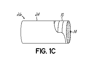
[0012] FIG. 1C is a partial view of a billet, which is a stack of the
graphene-
coated copper discs wrapped a copper foil in accordance with an embodiment of
the
present invention.
[0013] FIG. 1D is a schematic of a hot extrusion process to form a
monolithic
copper-graphene composite wire from the billet in accordance with an
embodiment
of the present invention.
[0014] FIG. 2 is a perspective view of a copper disc coated with a
graphene ink
in accordance with an embodiment of the present invention.
Detailed Description
[0015] Embodiments of the present invention are directed to ultra-
conductive
metal-graphene composite forms. For example, a metal component (e.g., a wire,
rod, bar, sheet, strip, film, or foil) may be coated with graphene and formed
into a
bulk form (e.g., a wire, rod, bar, sheet, strip, or foil). Further embodiments
are
directed to methods of synthesizing ultra-conductive metal-graphene composite
forms. As used herein, a "metal-graphene composite" refers to both composites
and
nano-alloys of the metal and graphene. In various embodiments, the metal may
be,
without limitation, copper, aluminum, silver, gold, titanium, nickel, iron,
magnesium,
manganese, cobalt, zinc, and chromium. Thus, while the embodiments described
below relate to ultra-conductive copper-graphene composites, the invention is
not so
limited.
[0016] In an aspect of the present invention, a metal-graphene composite
may
have enhanced electrical properties compared to a conventional metal component
with commercial grade purity. Conventional material behavior demonstrates that
electrical conductivity increases with metal purity and consequently decreases
with
alloy additions, second phase additives, and impurities. Such impurity
elements
manifest as solid solutions and/or second phases in the matrix metal during
processing, all of which decrease electrical properties (i.e., electrical
conductivity
and ampacity) of the bulk metal. However, in graphene, three of the four outer
shell
3
CA 03038523 2019-03-26
WO 2018/064137 PCT/US2017/053664
electrons are used to covalently bond within the hexagonal graphene plane. The
other electron is a pi (n) electron, which is highly mobile and is localized
over the
surface. The high inherent electrical properties of graphene may be attributed
to the
presence of this localized pi electron shell, which is somewhat analogous to
the 41
electron in copper. These electrons may work in tandem in a metal-graphene
composite, to produce enhanced electrical properties. Thus, an embodiment of
the
present invention includes a metal-graphene composite in bulk form, in which
single- or multi-layer graphene is distributed in the metal matrix and
primarily
oriented with the plane horizontal to the axial direction (but not
exclusively), which
produces ultra-conductivity and ultra-ampacity (i.e., conductivity above 100%
IACS
and greater ampacity than commercial grades).
[0017] With reference to FIGS. 1A-1D, in an embodiment, a method of
synthesizing an ultra-conductive copper-graphene composite form includes
forming
copper profiles and coating the copper profiles with graphene. As an example,
FIG.
1A, shows a copper rod 12 may be cut into copper discs 10 having a circular
cross
section. While the copper bulk form is shown in the form of a rod, it may have
other
forms such as sheet copper, copper foil, copper particles with micron or
nanoscale
diameters, and other bulk copper products. Similarly, while the copper
profiles are
shown in the form of discs, the profiles can have other cross-sectional shapes
including, without limitation, a rectangular cross-section, a square cross-
section, a
triangular cross-section, a hexagonal cross-section, etc. Further, forms of
the
copper profiles include, without limitation, copper pellets, shot, powder,
strips,
sheets, foils, films, wires, rods, bars, or particles. In an embodiment, the
copper rod
12 may be 00.625 inch in diameter and made of 4N purity (or typical UNS 10100
copper), and the copper discs 10 may have a thickness of approximately 0.125
in,
50 rim, 18 pm or less than 10 pm. The thickness of the copper profiles may be
as
small as 240 picometers (pm) (i.e., the covalent diameter of copper atoms) and
as
large as required, depending on the size of the desired precursor billet. The
cross-
sectional dimension (e.g., the diameter of a profile having a circular cross-
section) of
the profiles can be as small as 240 pm and as large as desired, depending on
the
size of the billet desired as well as the scale of the manufacturing
operation. Other
copper forms of various sizes can also be used in the production of the
precursor
composite copper billet. As previously described, the copper profiles may be
made
of another metal, such as aluminum, etc.
4
CA 03038523 2019-03-26
WO 2018/064137 PCT/US2017/053664
[0018] Next, the copper profiles may be coated with graphene. As shown in
FIG. 1B, in an embodiment, the copper discs 10 may be coated with graphene 14
via chemical vapor deposition (CVD) method. In an embodiment, the CVD method
may utilize a high temperature CVD apparatus 16 to deposit the graphene 14
directly onto the surface of the copper discs 10. In general, the CVD
apparatus
includes a large chamber with heating elements 18, and it is fitted with a
vacuum
pump (not shown) and several valves to feed the graphene precursor (e.g.,
coal,
coke, petroleum coke, graphite, methane or various hydrocarbons) along with
carrier gases (e.g., hydrogen, methane, carbon monoxide, noble gases, etc.) to
the
furnace. The copper discs 10 to be coated with graphene are placed on holders
22
inside the CVD chamber 18. The operating conditions of the chamber 18 are
maintained at prescribed temperature and pressure ranges, which are dependent
on
the precursor and carrier gases used, as well as the chamber material and
copper
profile dimensions. When graphene precursors and carrier gases are passed at
the
optimal CVD chamber operating conditions, single or multiple layers of
graphene
sheets in the form of hexagonally arranged sp2 bonded carbon atoms are formed
on
the copper profiles. The number of graphene layers may range from, for
example, 1
layer to 20 layers. The resulting graphene coating 14 may have a minimum
thickness of 120 pm (covalent diameter of carbon atoms).
[0019] Next, the graphene coated copper profiles may be arranged to form
a
precursor workpiece, which may have various forms such as a billet, rod,
plate, or
sheet. As shown in FIG. 10, the graphene-coated copper discs 10 are arranged
in a
preferred format. In the illustrated embodiment, the graphene-coated copper
discs
are wrapped in copper foil 24 to assemble a billet 26 of desired dimensions.
Although each of the copper discs 10 that form the billet 26 are shown having
a
graphene coating, it is not necessary for all the copper profiles used to make
the
billet to have a graphene coating on them. Further, a billet may be composed
of
copper profiles with different forms, sizes, and cross-sectional shapes, with
or
without graphene coating on the surface. For example, the billet can also be
comprised of CVD coated copper pellets, shots, powder, sheets, foils, wires,
rods,
or any combination of coated and uncoated forms to produce the composite
copper
billet (i.e., the yet un-formed or un-extruded precursor workpiece). Referring
to FIG.
1D, a hot extrusion device 28 may be used to hot-press and extrude the billet
26 to
form a bulk form of the composite. Hot-pressing may occur at temperatures up
to
5
CA 03038523 2019-03-26
WO 2018/064137
PCT/US2017/053664
900 00 and may include applying pressures up to 50 kpsi to the precursor
workpiece. The bulk form may also be formed from the precursor workpiece using
other mechanical processes such as cold-pressing at ambient temperature,
rolling,
or drawing. Cold-pressing may occur at ambient temperature and may include
applying pressures up to 75 kpsi to the precursor workpiece. The extrusion or
other
forming of the precursor workpiece into the bulk form may be conducted in an
inert
environment (e.g., in a nitrogen atmosphere). For example, the billet 26 may
be
formed into a wire 30 (or other profile shape) made of ultra-conductive copper
that
has a diameter of about 0.0808 in (12 AWG wire) and has a length of about 12
inches. Note that wires of much longer or smaller lengths, and larger or
smaller
diameters can be produced in a manufacturing scenario with larger billets. The
extruded bulk forms can have virtually any dimension and shape depending on
the
dies used during extrusion. Other extruded profiles can differ in size and
shape,
including rods, bars, plates, strands, tubes, and strips, for example. During
the
fabrication and extrusion of the billet 26, the graphene 14 becomes
distributed in the
copper matrix and is primarily (but not exclusively) oriented with a graphene
plane
being horizontal to an axial direction of the extruded form 30. As described
above,
metal-graphene composites other than a copper-graphene composite may be
formed using this method.
[0020] It
should be recognized that other forms of depositing graphene on the
copper may be used. For example, with reference to FIG. 2, in an embodiment,
the
graphene ink method may be used to deposit graphene sheets onto the surfaces
of
copper profiles at room temperature. In this method, single atomic layer or
multiple
atomic layer thick graphene sheets are mixed with stabilizing agents (also
called
surfactants), solvents, or suspension fluids to form a graphene ink 32, which
is
coated onto the copper discs 10. The stabilizing agent may include, without
limitation, ethanol, isopropanol, acetone, hexanes, water, or
dimethylformamide.
The copper discs 10 are then dried in convective air, which facilitates the
evaporation of the stabilizing agent leaving behind graphene coated copper
discs
10. The convective environment may consist of other gases than ambient air.
For
example, in an embodiment, the graphene ink can be dried in an environment
that
can be made of, without limitation, vacuum, argon, nitrogen, hydrogen, or a
combination of gases. The copper disc 10 may be placed in a fume hood at room
temperature to accelerate the evaporation of the stabilizing agents. The
resulting
6
CA 03038523 2019-03-26
WO 2018/064137 PCT/US2017/053664
graphene-coated copper profile may have a graphene layer of minimum thickness
of
120 pm and with no restriction on the maximum thickness.
[0021] The weight percentage of the graphene in the copper-graphene
composite may vary. At a minimum, the amount of graphene must be sufficient to
improve the electrical properties of the metal. For example, the weight
percentage of
the graphene may range from greater than 0 and up to and including 50%. In an
embodiment, the copper-graphene composite may include 0.00000001% to 50% by
weight of graphene, 0.05% to 30% by weight of graphene, 0.01% to 5% by weight
of
graphene, with a preferred range of from greater than zero up to and including
1%.
The balance of the copper-graphene composite is primarily copper but may
include
trace amounts of other elements (such as impurity elements already present in
the
copper profile). The copper may include, without limitation, UNS 10100,
UNS11000,
UNS 12200, or ultra-pure copper as well as other copper alloys. Examples of
the
bulk forms of the copper-graphene composite, with embedded graphene include,
without limitation, a wire, a rod, a tube, a strand, a strip, a foil, a plate,
or a bar.
[0022] The resulting ultra-conductive metal-graphene composite form
(e.g., the
wire 30) may have a similar or increased electrical conductivity compared to
the
IACS standard and may have an increased ampacity. For example, an ultra-
conductive copper wire or other bulk form according to the present invention
may
have an electrical conductivity of from about 57.6 MS/m (99.3% IACS) to about
60.90 MS/m (105% IACS) or greater, and an ampacity of about 19.1 MA/m2 at a
temperature of 60 C, or greater. The ultra-conductive copper bulk form may
have a
higher ampacity compared to the IACS standard at temperatures of from 20 C to
150 C. The corresponding values for commercially available copper wire
procured
from CerroWire LLC are 57.82 MS/m (99.69% IACS) and 3 to 4 MA/m2 at a
temperature of 20 C and 15.9 MA/m2 at 60 C. The corresponding values for
commercially available copper wire procured from South Wire LLC are 56.91 MS/m
(98.11% IACS) and 3 to 4 MA/m2 at a temperature of 20 C and 15.9 MA/m2 at
60 C. For another example, an ultra-conductive aluminum wire or other bulk
form
according to the present invention may have an electrical conductivity of
greater
than 34.5 MS/m (59.58% IACS), or about 34.76 MS/m (59.93% IACS). The
corresponding values for an aluminum wire made from commercially available
AA1100 was 34.5 MS/m (59.58% IACS).
7
CA 03038523 2019-03-26
WO 2018/064137
PCT/US2017/053664
[0023] In order to facilitate a more complete understanding of the
embodiments
of the invention, the following non-limiting examples are provided.
Example 1
[0024] A copper rod that was 0.625 inch in diameter and made of 4N purity
(or
typical UNS 10100 copper) was cut into discs with circular cross section and
approximately 0.125 in thickness. Next, the copper discs were placed in a bath
of
acetic acid for 1 minute to clean the surface of the copper discs.
[0025] Next, a graphene layer was deposited directly onto the face of the
copper discs via chemical vapor deposition (CVD). The copper discs were placed
flat on the sides of a quartz holder and introduced into the CVD chamber. A
vacuum
of less than 50 milliTorrs (mTorr) was achieved in the CVD chamber. The quartz
chamber was then flooded with hydrogen gas for another 15 minutes at
100 cm3/min to purge any remaining oxygen, while periodically checking for
hydrogen leaks. The furnace was heated to a range of about 900 C to 1100 C
for
16 to 25 minutes. During this heating, the quartz holder with copper discs was
positioned in the center of the CVD chamber for heating. Once the final
temperature
was reached in the furnace, it was maintained for an additional 15 to 30
minutes to
ensure the copper discs reached equilibrium temperature with the furnace
environment. A graphene precursor gas, comprising of processed methane along
with carrier gases (e.g., hydrogen, methane, carbon monoxide, noble gases) was
then introduced into the CVD chamber at a rate of at 0.1 liters per minute
(I/min) for
to 10 minutes during which graphene was deposited onto the copper disc
surfaces. Oxides and impurities were removed from the copper disc surfaces in
the
CVD chamber prior to graphene deposition facilitated by the high temperature
and
reducing atmosphere in the CVD chamber. Additionally, the deposition of
graphene
sealed the surfaces of the copper disc, thereby minimizing any further
oxidation
prior to subsequent processing. The copper discs were then reclaimed, stacked,
and wrapped in copper foil to assemble a billet of approximately 1 to 2 in in
length.
[0026] The billet was placed in an experimental extrusion apparatus at
700 C
to 800 C and hot-pressed for about 30 minutes with a force of 10,000 lb
(providing
a pressure of about 29,000 psi) prior to extrusion. It should be recognized
that the
force can be increased for larger billet sizes. A continuous flow of nitrogen
gas was
maintained to the apparatus during this step to minimize oxidation of the
billet. The
billet was then extruded at that temperature into a nitrogen gas environment
to form
8
CA 03038523 2019-03-26
WO 2018/064137 PCT/US2017/053664
the consolidated copper-graphene composite wire. The billet was formed into a
wire
of approximately 0.0808 in diameter (12 AWG wire) and approximately 24 in
length
(limited by the length of the billet).
[0027] The electrical conductivity and ampacity of the hot-extruded 12
AWG
copper-graphene composite wire was measured according to ASTM standards and
was reported to be 60.73 MS/m (104.7% IACS) at 20 C and 19.1 MA/m2 at 60 C,
respectively. The corresponding values for commercially available copper wire
procured from CerroWire LLC are 57.82 MS/m (99.69% IACS) and 3 to 4 MA/m2 at
a temperature of 20 C and 15.9 MA/m2 at 60 C. The corresponding values for
commercially available copper wire procured from South Wire LLC are 56.91 MS/m
(98.11% IACS) and 3 to 4 MA/m2 at a temperature of 20 C and 15.9 MA/m2 at
60 C.
Example 2
[0028] Copper discs were prepared according to the method described in
Example 1. Next, graphene ink was coated on the transverse circular surfaces
of
the discs. The copper-graphene composite included 0.5% by weight of graphene.
To create the graphene ink, 2 mL of isopropanol was mixed with the graphene
sheets to achieve a mixture. The copper discs were coated with the graphene-
isopropanol ink and placed in a fume hood at room temperature to evaporate the
isopropanol. The coated discs were then reclaimed, stacked, and wrapped in a
copper foil to assemble a billet with a length of approximately 1 to 2 in. The
billet
was extruded into a wire according to the method described in Example 1.
[0029] The electrical conductivity and ampacity of the hot-extruded 12
AWG
copper-graphene composite wire was measured according to ASTM standards, and
is reported to be 57.6 MS/m (99.3% IACS) and 19.1 MA/m2 at 60 C, respectively.
The corresponding values for commercially available copper wire procured from
CerroWire LLC are 57.82 MS/m (99.69% IACS) and 3 to 4 MA/m2 at a temperature
of 20 C and 15.9 MA/m2 at 60 C. The corresponding values for commercially
available copper wire procured from SouthWire LLC are 56.91 MS/m (98.11% IACS)
and 3 to 4 MA/m2 at a temperature of 20 C and 15.9 MA/m2 at 60 C.
[0030] While specific embodiments have been described in considerable
detail
to illustrate the present invention, the description is not intended to
restrict or in any
way limit the scope of the appended claims to such detail. The various
features
discussed herein may be used alone or in any combination. Additional
advantages
9
CA 03038523 2019-03-26
WO 2018/064137 PCT/US2017/053664
and modifications will readily appear to those skilled in the art. The
invention in its
broader aspects is therefore not limited to the specific details,
representative
apparatus and methods and illustrative examples shown and described.
Accordingly, departures may be made from such details without departing from
the
scope of the general inventive concept.
Example 3
[0031] Discs of 0.625 in diameter were punched from an aluminum alloy
sheet
made of AA1100. Next, graphene ink was coated on the transverse circular
surfaces
of the discs. The aluminum-graphene composite included 0.25% by weight of
graphene. To create the graphene ink, 2 mL of isopropanol was mixed with the
graphene sheets to achieve a mixture. The aluminum discs were coated with the
graphene-isopropanol ink and placed in a fume hood at room temperature to
evaporate the isopropanol. The coated discs were then reclaimed, stacked, and
wrapped in a pure aluminum foil to assemble a billet with a length of
approximately
1 to 2 in. The billet was placed in an experimental extrusion apparatus at 350
C to
550 C and hot-pressed for about 30 minutes with a force of 3,000 lb
(providing a
pressure of about 8,500 psi) prior to extrusion. It should be recognized that
the force
can be increased for larger billet sizes. A continuous flow of nitrogen gas
was
maintained to the apparatus during this step to minimize oxidation of the
billet. The
billet was then extruded at that temperature into a nitrogen gas environment
to form
the consolidated aluminum-graphene composite wire. The billet was formed into
a
wire of approximately 0.0808 in diameter (12 AWG wire) and approximately 24 in
length (limited by the length of the billet).
[0032] The electrical conductivity and ampacity of the hot-extruded 12
AWG
aluminum-graphene composite wire was measured according to ASTM standards
and was reported to be 34.76 MS/m (59.93% IACS). Control wires made of AA1100
without graphene measured to have an electrical conductivity of 34.5 MS/m
(59.58%
IACS).
[0033] While specific embodiments have been described in considerable
detail
to illustrate the present invention, the description is not intended to
restrict or in any
way limit the scope of the appended claims to such detail. The various
features
discussed herein may be used alone or in any combination. Additional
advantages
and modifications will readily appear to those skilled in the art. The
invention in its
broader aspects is therefore not limited to the specific details,
representative
CA 03038523 2019-03-26
WO 2018/064137
PCT/US2017/053664
apparatus and methods and illustrative examples shown and described.
Accordingly, departures may be made from such details without departing from
the
scope of the general inventive concept.
11