Note: Descriptions are shown in the official language in which they were submitted.
CA 03038874 2019-03-29
WO 2018/060726 PCT/GB2017/052928
1
SECURITY DEVICES
This invention relates to security devices. Security devices are used for
example
on documents of value such as banknotes, cheques, passports, identity cards,
certificates of authenticity, fiscal stamps and other secure documents, in
order to
confirm their authenticity. Methods for their manufacture will also be
described.
Articles of value, and particularly documents of value such as banknotes,
cheques, passports, identification documents, certificates and licences, are
frequently the target of counterfeiters and persons wishing to make fraudulent
copies thereof and/or changes to any data contained therein. Typically such
objects are provided with a number of visible security devices for checking
the
authenticity of the object. By "security device" we mean a feature which it is
not
possible to reproduce accurately by taking a visible light copy, e.g. through
the
use of standardly available photocopying or scanning equipment. Examples
include features based on one or more patterns such as microtext, fine line
patterns, latent images, venetian blind devices, lenticular devices, moire
interference devices and moire magnification devices, each of which generates
a
secure visual effect. Other
known security devices include holograms,
watermarks, embossings, perforations and the use of colour-shifting or
luminescent / fluorescent inks. Common to all such devices is that the visual
effect exhibited by the device is extremely difficult, or impossible, to copy
using
available reproduction techniques such as photocopying. Security devices
exhibiting non-visible effects such as magnetic materials may also be
employed.
One class of security devices are those which produce an optically variable
effect, meaning that the appearance of the device is different at different
angles
of view. Such
devices are particularly effective since direct copies (e.g.
photocopies) will not produce the optically variable effect and hence can be
readily distinguished from genuine devices. Optically variable effects can be
generated based on various different mechanisms, including holograms and
other diffractive devices, moire interference and other mechanisms relying on
parallax such as venetian blind devices, and also devices which make use of
CA 03038874 2019-03-29
WO 2018/060726 PCT/GB2017/052928
2
focusing elements such as lenses, including moire magnifier devices, integral
imaging devices and so-called lenticular devices.
Moire magnifier devices (examples of which are described in EP-A-1695121,
WO-A-94/27254, WO-A-2011/107782 and W02011/107783) make use of an
array of focusing elements (such as lenses or mirrors) and a corresponding
array of microimages, wherein the pitches of the focusing elements and the
array of microimages and/or their relative locations are mismatched with the
array of focusing elements such that a magnified version of the microimages is
generated due to the moire effect. Each microimage is a complete, miniature
version of the image which is ultimately observed, and the array of focusing
elements acts to select and magnify a small portion of each underlying
microimage, which portions are combined by the human eye such that the
whole, magnified image is visualised. This mechanism is sometimes referred to
as "synthetic magnification". The magnified array appears to move relative to
the
device upon tilting and can be configured to appear above or below the surface
of the device itself. The degree of magnification depends, inter alia, on the
degree of pitch mismatch and/or angular mismatch between the focusing
element array and the microimage array.
Integral imaging devices are similar to moire magnifier devices in that an
array of
microimages is provided under a corresponding array of lenses, each
microimage being a miniature version of the image to be displayed. However
here there is no mismatch between the lenses and the microimages. Instead a
visual effect is created by arranging for each microimage to be a view of the
same object but from a different viewpoint. When the device is tilted,
different
ones of the images are magnified by the lenses such that the impression of a
three-dimensional image is given.
"Hybrid" devices also exist which combine features of moire magnification
devices with those of integral imaging devices. In a "pure" moire
magnification
device, the microimages forming the array will generally be identical to one
another. Likewise in a "pure" integral imaging device there will be no
mismatch
CA 03038874 2019-03-29
WO 2018/060726 PCT/GB2017/052928
3
between the arrays, as described above. A "hybrid" moire magnification /
integral imaging device utilises an array of microimages which differ slightly
from
one another, showing different views of an object, as in an integral imaging
device. However, as in a moire magnification device there is a mismatch
between the focusing element array and the microimage array, resulting in a
synthetically magnified version of the microimage array, due to the moire
effect,
the magnified microimages having a three-dimensional appearance. Since the
visual effect is a result of the moire effect, such hybrid devices are
considered a
subset of moire magnification devices for the purposes of the present
disclosure.
In general, therefore, the microimages provided in a moire magnification
device
should be substantially identical in the sense that they are either exactly
the
same as one another (pure moire magnifiers) or show the same object/scene but
from different viewpoints (hybrid devices).
Moire magnifiers, integral imaging devices and hybrid devices can all be
configured to operate in just one dimension (e.g. utilising cylindrical
lenses) or in
two dimensions (e.g. comprising a 2D array of spherical or aspherical lenses).
Lenticular devices on the other hand do not rely upon magnification, synthetic
or
otherwise. An array of focusing elements, typically cylindrical lenses,
overlies a
corresponding array of image sections, or "slices", each of which depicts only
a
portion of an image which is to be displayed. Image slices from two or more
different images are interleaved and, when viewed through the focusing
elements, at each viewing angle, only selected image slices will be directed
towards the viewer. In this way, different composite images can be viewed at
different angles. However it should be appreciated that no magnification
typically
takes place and the resulting image which is observed will be of substantially
the
same size as that to which the underlying image slices are formed. Some
examples of lenticular devices are described in US-A-4892336, WO-A-
2011/051669, WO-A-2011051670, WO-A-2012/027779 and US-B-6856462.
More recently, two-dimensional lenticular devices have also been developed and
examples of these are disclosed in British patent application numbers
1313362.4
and 1313363.2. Lenticular devices have the advantage that different images
CA 03038874 2019-03-29
WO 2018/060726 PCT/GB2017/052928
4
can be displayed at different viewing angles, giving rise to the possibility
of
animation and other striking visual effects which are not possible using the
moire
magnifier or integral imaging techniques.
Security devices such as moire magnifiers, integral imaging devices and
lenticular devices depend for their success significantly on the resolution
with
which the image array (defining for example microimages, interleaved image
sections or the like) can be formed. Since the security device must be thin in
order to be incorporated into a document such as a banknote, the focusing
elements must also be thin, which by their nature also limits their lateral
dimensions. For example, lenses used in such security elements preferably
have a width or diameter of 50 microns or less, e.g. 30 microns. In a
lenticular
device this leads to the requirement that each image element must have a width
which is at most half the lens width. For example, in a "two channel"
lenticular
switch device which displays only two images (one across a first range of
viewing angles and the other across the remaining viewing angles), where the
lenses are of 30 micron width, each image section must have a width of 15
microns or less. More complicated lenticular effects such as animation, motion
or 3D effects usually require more than two interlaced images and hence each
section needs to be even finer in order to fit all of the image sections into
the
optical footprint of each lens. For instance, in a "six channel" device with
six
interlaced images, where the lenses are of 30 micron width, each image section
must have a width of 5 microns or less.
Similarly high-resolution image elements are also required in moire magnifiers
and integral imaging devices since approximately one microimage must be
provided for each focusing element and again this means in effect that each
microimage must be formed within a small area of e.g. 30 by 30 microns. In
order for the microimage to carry any detail, fine linewidths of 5 microns or
less
are therefore highly desirable.
Typical processes used to manufacture image patterns for security devices are
based on printing and include intaglio, gravure, wet lithographic printing as
well
CA 03038874 2019-03-29
WO 2018/060726 PCT/GB2017/052928
as dry lithographic printing. The achievable resolution is limited by several
factors, including the viscosity, wettability and chemistry of the ink, as
well as the
surface energy, unevenness and wicking ability of the substrate, all of which
lead
to ink spreading. With careful design and implementation, such techniques can
5 be used to print pattern elements with a line width of between 25 pm and
50 pm.
For example, with gravure or wet lithographic printing it is possible to
achieve
line widths down to about 15 pm.
Methods such as these are limited to the formation of single-colour image
elements, since it is not possible to achieve the high registration required
between different workings of a multi-coloured print. In the case of a
lenticular
device for example, the various interlaced image sections must all be defined
on
a single print master (e.g. a gravure or lithographic cylinder) and
transferred to
the substrate in a single working, hence in a single colour. The various
images
displayed by the resulting security device will therefore be monotone, or at
most
duotone if the so-formed image elements are placed against a background of a
different colour.
One approach which has been put forward as an alternative to the printing
techniques mentioned above is used in the so-called Unison MotionTM product
by Nanoventions Holdings LLC, as mentioned for example in WO-A-
2005052650. This involves creating pattern elements ("icon elements") as
recesses in a substrate surface before spreading ink over the surface and then
scraping off excess ink with a doctor blade. The resulting inked recesses can
be
produced with line widths of the order of 2 pm to 3 pm. This high resolution
produces a very good visual effect, but the process is complex and expensive.
Further, limits are placed on the minimum substrate thickness by the
requirement to carry recesses in its surface. Again, this technique is only
suitable for producing image elements of a single colour.
Some more methods for generating patterns or micropatterns (i.e. image arrays)
on a substrate are known from US 2009/0297805 Al and WO 2011/102800 Al.
These disclose methods of forming micropatterns in which a die form or matrix
is
CA 03038874 2019-03-29
WO 2018/060726 PCT/GB2017/052928
6
provided whose surface comprises a plurality of recesses. The recesses are
filled with a curable material, a treated substrate layer is made to cover the
recesses of the matrix, the material is cured to fix it to the treated surface
of the
substrate layer, and the material is removed from the recesses by separating
the
substrate layer from the matrix.
Another method of forming a micropattern is disclosed in WO 2014/070079 Al.
Here it is taught that a matrix is provided whose surface comprises a
plurality of
recesses, the recesses are filled with a curable material, and a curable
pickup
.. layer is made to cover the recesses of the matrix. The curable pickup layer
and
the curable material are cured, fixing them together, and the pickup later is
separated from the matrix, removing the material from the recesses. The pickup
layer is, at some point during or after this process, transferred onto a
substrate
layer so that the pattern is provided on the substrate layer.
Other approaches involve the patterning of a metal layer through the use of a
photosensitive resist material and exposing the resist to appropriate
radiation
through a mask. Depending on the nature of the resist material, exposure to
the
radiation either increases or decreases its solubility in certain etchants,
such that
the pattern on the mask is transferred to the metal layer when the resist-
covered
metal substrate is subsequently exposed to the etchant. For instance, EP-A-
0987599 discloses a negative resist system in which the exposed photoresist
becomes insoluble in the etchant upon exposure to ultraviolet light. The
portions
of the metal layer underlying the exposed parts of the resist are thus
protected
from the etchant and the final pattern formed in the metal layer is the
"negative"
of that carried on the mask. In contrast, our British patent application no.
1510073.9 discloses a positive resist system in which the exposed photoresist
becomes more soluble in the etchant upon exposure to ultraviolet light. The
portions of the metal layer underlying the unexposed parts of the resist are
thus
protected from the etchant and the final pattern formed in the metal layer is
the
same as that carried on the mask. Methods such as these offer good pattern
resolution, but still impose restrictions on the number and arrangement of
colours that can be exhibited.
CA 03038874 2019-03-29
WO 2018/060726 PCT/GB2017/052928
7
Security devices with new and distinctive appearances are constantly sought in
order to keep ahead of would-be counterfeiters.
In accordance with a first aspect of the present invention, a security device
cornprises:
an array of focussing elements with regular periodicity in at least a first
direction, each focusing element having an optical footprint of which
different
portions will be directed to the viewer in dependence on the viewing angle;
and
an array of image elements with regular periodicity in at least the first
direction overlapping the array of focusing structures, the image elements
representing portions of at least two respective images, and at least one
image
element from each respective image being located in the optical footprint of
each
focusing structure;
wherein the security device includes a first region and a second region
which is laterally offset from the first, the image elements in the first
region being
laterally shifted in at least the first direction relative to the image
elements in the
second region such that, at a first viewing angle, in the first region of the
device
the focussing structures direct image elements corresponding to a first image
to
the viewer such that the first image is displayed across the first region of
the
device, and simultaneously, in the second region of the device, the focussing
structures direct image elements corresponding to a second image to the viewer
such that the second image is displayed across the second region of the
device,
and at a second viewing angle the second image is displayed across the first
region of the device and simultaneously the first image is displayed across
the
second region of the device;
and where the security device further comprises a colour filter located in
use between the image elements and the viewer, the colour filter overlapping
at
least part of the array of focussing elements and the array of image elements,
and having a first colour in the first region of the device and a different
colour in
the second region of the device such that the colour appearance of the first
and
second images is different in the respective first and second regions of the
device.
CA 03038874 2019-03-29
WO 2018/060726 PCT/GB2017/052928
8
In common with other aspects of the present invention to be described below,
the security device here comprises a colour filter which introduces additional
colour effects, and hence imparts a new and more complex appearance to the
device. As will be detailed hereinafter, the colour filter could be provided
as an
extra component additional to those mentioned already but could alternatively
be
incorporated into one of the existing components, such as the focussing
element
array itself. What is important is that the colour filter sits between the
image
array and the viewer in use so as to modify the apparent colour of the image
array. The colour filter will typically be formed of transparent materials at
least
one of which contains a visibly coloured tint so that only selected
wavelengths of
the visible spectrum are transmitted therethrough.
The device is divided into at least first and second (and optionally further)
regions which are laterally offset from one another meaning in this context
that
they occupy different portions (non-overlapping) of the device area. The
colour
filter is of a different colour in the first region as compared with in the
second
region. The term "colour" is used herein to denote any hue which is
recognisable to human vision, including achromatics such as black, grey,
white,
silver and the like, as well as chromatics such as red, green, blue, orange
etc.
One of the regions of the colour layer could also be colourless (i.e. not
modify
the apparent colour of the image elements transmitted therethrough) since this
will be distinguishable to the human eye from the neighbouring region(s) and
therefore have the desired effect of forming a more complex security effect
across the device as a whole. These considerations apply to all aspects of the
presently disclosed invention.
It will be appreciated that there may be any number of regions each with
different phase shifts and similarly more than two images may be provided. For
instance, a third region may simultaneously display a third image.
In this first aspect of the invention, the security device is a lenticular
device
which will display different images at different viewing angles. Each image
could
take any desirable form, e.g. a uniform block colour, indicia such as
CA 03038874 2019-03-29
WO 2018/060726 PCT/GB2017/052928
9
alphanumerical text, a line pattern or any other graphic. The array of image
elements is configured to co-operate with the focussing elements to generate
the
optically variable lenticular effect across the device. However, in the first
region
of the device the arrangement of image elements is laterally shifted ("phase
.. shifted") relative to the arrangement of image elements in the second
region.
This has the result that the device will display different ones of the images
in the
first and second regions respectively, simultaneously (i.e. at one viewing
angle).
By arranging the different images to be displayed in the same two respective
regions as those in which the colour of the colour layer differs, a
particularly
complex optical effect is achieved since each region will display the same two
images but at different viewing angles and, significantly, in different
colours for
each region. The register required between the colour layer and the image
element array to achieve this presents a significant challenge to the would-be
counterfeiter and any mis-register will be readily apparent. Further,
imitating the
end result through other means will also be extremely difficult: for example,
producing the image elements in different colours in the first and second
regions
would require a multi-coloured image array which as discussed above presents
substantial manufacturing obstacles.
In preferred embodiments, the image array comprises a set of monochromatic
image elements corresponding to the first image in the first and second
regions
of the device. That is, the first image elements are of the same colour in
both
regions. As mentioned above forming a monochromatic image array simplifies
the manufacturing process since a relatively wide range of suitable printing
techniques and the like are available. In some preferred embodiments, the
monochromatic image elements are substantially opaque and preferably
reflective, e.g. formed of a dark material such as black ink or of a metal
layer
such as aluminium, which is particularly well suited to viewing in reflect
light. In
other preferred implementations, the monochromatic image elements are semi-
.. transparent or translucent in which case the device may be best suited to
viewing in transmission. Advantageously, the colour of the monochromatic
image elements is different to the colours of the colour filter in both the
first and
second regions of the device. This will give rise to a greater number of
colours
CA 03038874 2019-03-29
WO 2018/060726 PCT/GB2017/052928
visible from the end device as a whole. In other preferred implementations,
the
colour of the monochromatic image elements substantially matches the colour of
the colour filter in one of the first and second regions of the device. This
can
give rise to additional security effects as discussed in relation to the
second
5 aspect of the invention below.
In some preferred embodiments, the image elements corresponding to the
second image are defined by colourless gaps between the monochromatic
image elements corresponding to the first image. Thus the second image will be
10 a uniform block area with a colour determined solely by the colour
filter, which
will lead to different appearances thereof in the first and second regions. In
other preferred embodiments, the image elements corresponding to the second
image are defined by a second set of monochromatic image elements in the first
and second regions of the device having a different colour from those
corresponding to the first image. This can be used to introduce yet further
colours and hence increase the complexity of the device still further.
The security device could be a one-dimensional or two-dimensional lenticular
device. In the former case, the array of focussing elements preferably
comprises an array of elongate focussing element structures extending along a
second direction which is orthogonal to the first direction, and the image
elements comprise elongate image slices extending along the second direction.
The elongate focussing element structures could be individual elongate
focussing elements such as cylindrical lenses or could each be formed of a
plurality of focussing elements which need not individually be elongate, e.g.
spherical lenses. For a two-dimensional lenticular device the focussing
element
array may comprise spherical or aspherical focussing elements arranged on an
orthogonal or hexagonal grid for instance, and the image elements could be
e.g.
dots or squares.
A second aspect of the present invention provides a security device,
comprising:
CA 03038874 2019-03-29
WO 2018/060726 PCT/GB2017/052928
11
an array of focussing elements with regular periodicity in at least a first
direction, each focusing element having an optical footprint of which
different
portions will be directed to the viewer in dependence on the viewing angle;
and
a corresponding first image array overlapping the array of focussing
elements and configured to co-operate with the array of focussing elements so
as to generate a first optically variable effect which varies with viewing
angle, the
first image array comprising a periodic arrangement of image elements or
microimages formed in a first colour across the security device;
wherein the security device further comprises a colour filter located in use
between the first image array and the viewer, the colour filter overlapping at
least
part of the array of focussing elements and the first image array, and having
different colours in respective first and second regions of the device which
are
laterally offset from one another, the colour of the colour filter layer in
the first
region of the device substantially matching the first colour of the image
elements
or microimages.
Again, the colour filter can be provided in various different ways as
mentioned
above in relation to the first aspect of the invention. By matching the colour
of
the colour filter to that of the image elements or microimages in a first
region of
the device, various new optical effects can be achieved as a result of
effectively
reducing or removing the colour contrast between the image elements or
microimages and their surroundings. The effects can take the form of changing
the number of colours that are displayed by the device, or even inhibiting the
first
optically variable effect in the first region. It should be noted that the
security
device of the second aspect of the invention is not limited to operating as a
lenticular device but alternatively be a moire magnification device or a moire
magnifier, for example.
Hence in a first preferred embodiment, the first image array further comprises
a
background surrounding the image elements or microimages which is
substantially colourless. For instance the background might be reflective
uniformly across substantially all visible wavelengths (e.g. white or mirror-
like
silver), or could be optically clear (i.e. transparent with no visible tint).
In this
CA 03038874 2019-03-29
WO 2018/060726 PCT/GB2017/052928
12
way the colour layer in the first region will effectively conceal the image
elements
or microimages since they will appear in the same colour as the background. As
a result the first optically variable effect is exhibited in the second region
and
substantially not in the first region. This has the strong benefit that the
effective
optically active zone of the device can be controlled through design of the
colour
filter alone and does not require modification to the image array or focussing
element array.
In other cases it may be preferred if the first image array further comprises
a
background surrounding the image elements or microimages which is of a
second colour, the colour of the colour filter layer in the second region of
the
device substantially matching the second colour. Such arrangements can be
utilised to generate additional colours as the device is tilted of which
examples
will be given below.
In an especially preferred embodiment, the security device further comprises a
second image array overlapping the array of focussing elements and configured
to co-operate with the array of focussing elements so as to generate a second
optically variable effect which varies with viewing angle, the second image
array
comprising a periodic arrangement of image elements or microimages formed in
a second colour across the security device. Both the first and second image
arrays can, if desired, extend across the whole area of the device. If the
background is colourless, as mentioned above, in the first region the first
image
array will effectively be inhibited whilst the second image array will be
visible
since its elements or microimages will not match the colour of the colour
filter
and hence will show a contrast with their surroundings. The colour of the
second image array could differ from both the colours of the colour filter in
the
first and second regions in which case the second optically variable effect
will be
visible in both regions. However, most preferably, the colour of the colour
filter
layer in the second region of the device substantially matches the second
colour
of the image elements or microimages. Hence preferably, in the second region
of the device the image elements or microimages are substantially concealed
from view by the matching colours of the image elements or microimages and
CA 03038874 2019-03-29
WO 2018/060726 PCT/GB2017/052928
13
the colour filter, such that the second optically variable effect is exhibited
in the
first region and substantially not in the second region.
In this way the optically active areas of the device can be defined by the
lateral
arrangement of the colour filter alone, which is used to selectively inhibit
the
optical effect generated by one image array in one region so that another
dominates the appearance there, and vice versa in other region(s) of the
device.
The optically variable effects generated by each image array could be of the
same type (e.g. lenticular or moire magnifier) or could be a mixture of
different
types. In the case of multiple lenticular devices, the images incorporated
into
each image array could be the same or different, and likewise in the case of
multiple moire magnifier devices or similar the microimages could be the same
or different. The apparent depth and magnification level of a moire magnified
image could also be different for the two image arrays, achieved by selecting
a
different pitch or rotational orientation for each array.
A third aspect of the present invention provides a security device,
comprising:
an array of focussing elements with regular periodicity in at least a first
direction, each focusing element having an optical footprint of which
different
portions will be directed to the viewer in dependence on the viewing angle;
and
a corresponding first image array overlapping the array of focussing
elements and configured to co-operate with the array of focussing elements so
as to generate a first optically variable effect which varies with viewing
angle, the
first image array comprising a periodic arrangement of image elements or
microimages formed in a first colour across the security device;
wherein the security device further comprises a colour filter located in use
between the first image array and the viewer, the colour filter overlapping at
least
part of the array of focussing elements and the first image array, and having
different colours in respective first and second regions of the device which
are
laterally offset from one another, the colour of the colour filter layer in
the first
region of the device being complementary to the first colour of the image
elements or microimages.
CA 03038874 2019-03-29
WO 2018/060726 PCT/GB2017/052928
14
Again, the device according to the third aspect of the invention makes use of
a
multi-coloured colour filter which can be provided in any of the ways
mentioned
above or below. In this case the colour filter includes a region in which its
colour
is complementary to the colour of the image elements or microimages forming
the image array. A complementary colour is one which combines with its
counterpart colour to effectively block the transmission of substantially all
visible
wavelengths. Depending on the construction of the device a number of
beneficial effects can be achieved, including enhancing the visible contrast
between the image elements and their surroundings so as to make the optically
variable effect more distinct in the first region. This may either be in terms
of the
contrast between a microimage and its adjacent background (visible
simultaneously) in a moire magnifier or in terms of the contrast seen between
different images (viewed sequentially) as a lenticular device is tilted, for
example.
In preferred embodiments, the first image array further comprises a background
surrounding the image elements or microimages which is substantially
colourless. As above, this could in practice be white, reflective or clear for
instance. In other
preferred embodiments, the first image array further
comprises a background surrounding the image elements or microimages which
is of a second colour, the colour of the colour filter layer in the second
region of
the device being complementary to the second colour. This has the advantage
of also enhancing the visibility of the optical effect in the second region.
In accordance with a fourth embodiment of the invention, a security device
comprises:
an array of focussing elements with regular periodicity in at least a first
direction, each focusing element having an optical footprint of which
different
portions will be directed to the viewer in dependence on the viewing angle;
and
a corresponding first image array overlapping the array of focussing
elements and configured to co-operate with the array of focussing elements so
as to generate a first optically variable effect which varies with viewing
angle, the
CA 03038874 2019-03-29
WO 2018/060726 PCT/GB2017/052928
first image array comprising a periodic arrangement of image elements or
microimages formed in a first colour across the security device;
wherein the security device further comprises:
a colour filter located in use between the first image array and the viewer,
5 the colour filter overlapping at least part of the array of focussing
elements and
the first image array, and having different colours in respective first and
second
regions of the device which are laterally offset from one another; and
a backing layer located behind the first image array such that the first
image array is between the colour filter and the backing layer, the backing
layer
10 .. comprising at least two laterally offset areas of different colour, the
backing layer
being visible at least between the image elements or microimages in the first
image array.
Once again, the security device of the forth aspect of the invention makes use
of
15 a colour filter located between the viewer and the image array as in the
previous
aspects. However in this case the device further includes a backing layer
located on the other side of the image array which is also multi-coloured and
so
introduces yet more complex effects. The backing layer will be visible between
the image elements or microimages defined by the first image array in all
embodiments, and in some embodiments may also affect the apparent colour of
those image elements or microimages if they are formed of a semi-transparent
material. Hence in some preferred embodiments, the image elements or
microimages of the first image array are substantially opaque or reflective
such
that the backing layer does not contribute to their colour appearance. In
other
preferred embodiments, the image elements or microimages of the first image
array are semi-transparent such that their apparent colour (before the colour
filter is taken into account) results from a combination of the first colour
and the
colours of the backing layer.
The arrangement of areas forming the backing layer could be independent of the
arrangement of regions in the colour filter and the two components need not be
registered. However, in particularly preferred cases two of the differently
coloured areas of the backing layer correspond to the first and second regions
of
CA 03038874 2019-03-29
WO 2018/060726 PCT/GB2017/052928
16
the device respectively. This further increases the security level since any
mis-
register between the areas and regions will be immediately apparent. The
appearance of the device can be made still more complex if at least two of the
differently coloured areas of the backing layer are located in each of the
first and
second regions of the device. Selected boundaries of the areas and regions
may still coincide in order to demonstrate register.
The colours of the various areas in the backing layer could be different from
those in the colour filter in order to introduce a greater number of colours
to the
device. However, in other preferred examples, the colours of the backing layer
are the same as the colours of the colour filter.
As indicated above, the security devices of the second, third and fourth
embodiments, could operate on any mechanism in which an optically variable
effect is generated by the interaction between the focussing elements and the
image array upon changing the viewing angle. For example, the devices could
be lenticular devices, moire magnifiers or integral imaging devices and in
some
cases more than one such mechanism may be incorporated in a single device
as mentioned above.
Hence in some preferred embodiments, the first image array comprises a regular
microimage array and the pitches of the focusing element array and of the
microimage array and their relative orientations are such that the focusing
element array co-operates with the microimage array to generate a magnified
version of the microimage array due to the moire effect. (Moire magnifier)
In other preferred embodiments, the first image array comprises a regular
microimage array in which the microimages all depict the same object from a
different viewpoint, and the pitches and orientation of the focusing element
array
and of the microimage array are the same, such that the focusing element array
co-operates with the microimage array to generate a magnified, optically-
variable version of the object. (Integral imager)
CA 03038874 2019-03-29
WO 2018/060726 PCT/GB2017/052928
17
In other preferred embodiments, the array of focussing elements has regular
periodicity in at least a first direction, each focusing element having an
optical
footprint of which different portions will be directed to the viewer in
dependence
on the viewing angle; and the first image array comprises an array of image
elements with regular periodicity in at least the first direction, the image
elements
representing portions of at least two respective images, and at least one
image
element from each respective image being located in the optical footprint of
each
focusing structure, such that, at least in a portion of the device, at a first
viewing
angle, the focussing structures direct image elements corresponding to a first
image to the viewer such that the first image is displayed across the portion
of
the device, and at a second viewing angle the second image is displayed across
the portion of the device. (Lenticular device)
In the case of a lenticular security device, principles of the first aspect of
the
invention can advantageously be combined with those of the second, third and
fourth aspects. Hence, preferably, the image elements in the first region of
the
device are laterally shifted in at least the first direction relative to the
image
elements in the second region such that, at the first viewing angle, in the
first
region of the device the focussing structures direct image elements
corresponding to the first image to the viewer such that the first image is
displayed across the first region of the device, and simultaneously, in the
second
region of the device, the focussing structures direct image elements
corresponding to the second image to the viewer such that the second image is
displayed across the second region of the device, and at a second viewing
angle
the second image is displayed across the first region of the device and
simultaneously the first image is displayed across the second region of the
device, the colour appearance of the first and second images being different
in
the respective first and second regions of the device.
As indicated above, in all aspects of the invention the colour filter can be
implemented in various different ways with substantially the same result. The
colour filter may be provided as a further component in addition to those
already
referenced, or may be formed integrally with one or more of those components.
CA 03038874 2019-03-29
WO 2018/060726 PCT/GB2017/052928
18
For instance, in a preferred embodiment, the colour filter is formed at least
in
part by the focussing elements of the focussing element array having different
colours from one another in the respective first and second regions of the
device.
In another preferred embodiment, the colour filter is formed at least in part
by a
pedestal layer provided between the focussing element array and a surface of a
substrate on which the focussing element array is located, the pedestal layer
comprising at least first and second transparent materials of different
colours
from one another in the respective first and second regions of the device.
In yet another preferred embodiment, the colour filter is formed at least in
part by
an image base layer provided between the image array and a surface of a
substrate on which the image array is formed, the image base layer comprising
at least first and second transparent materials of different colours from one
another in the respective first and second regions of the device. In this
case, the
image base layer is advantageously a tie-coat formed of curable materials for
affixing the image array to the substrate.
In another preferred embodiment, the colour filter is formed at least in part
by an
intermediate layer spaced from both the focussing element array and from the
image array. For example, the security device could comprise a plurality of
transparent substrates having the focussing element array and the image array
arranged on surfaces thereof with one or more intermediate interfaces between
substrates carrying the colour filter.
In a still further embodiment, the colour filter could be provided in an
adhesive
layer used to join components of the security device to one another. For
example, the focussing element array could be provided in the form of a
transfer
structure which is then affixed to a substrate via such an adhesive layer,
e.g. by
hot stamping. The adhesive layer can be formed in regions of different colour
to
achieve any of the aforementioned effects. The adhesive layer may be pre-
applied to the substrate or may form part of the transfer structure. In a
variant of
CA 03038874 2019-03-29
WO 2018/060726 PCT/GB2017/052928
19
this implementation, the adhesive layer could be colourless and a colour
filter
layer printed onto the substrate prior to application of the lens structure
thereover.
It should be noted that across the device as a whole the colour filter could
be
formed of more than one of the above options in combination with one another,
e.g. incorporating the filter using different ones of the above techniques in
different regions of the device. Alternatively or additionally, the colour
filter
comprises at least two colour filter layers provided at different spacings
from the
focussing element array and/or from the image array which are laterally offset
and preferably partially overlap one another. For instance across one portion
of
the device (which may or may not correspond to a specific region thereof) the
colour filter could be provided by an intermediate layer within the substrate
structure whereas across another portion (which may overlap with the first) it
may be provided by another intermediate layer at another location within the
substrate thickness.
Preferably, at least in a portion of the device the image array is located
substantially in the focal plane of the focussing element array. This ensures
that
a substantially focused image will be displayed by the end device. Typically,
the
focal plane will be at the same position across the whole device. However, in
preferred embodiments the complexity of the device can be further enhanced if
the position of the focal plane of the focussing element array is made
different in
the first and second regions of the device. This could be achieved for
instance
by varying the focal length of the focussing elements from one region to the
next,
e.g. by forming the focussing elements of different shapes, or by positioning
the
focussing elements at different levels, e.g. through the use of pedestal
layers
under the focussing element array with different heights in each region.
In preferred embodiments, each focusing element comprises any of: a
cylindrical
focusing element, a spherical focussing element or an aspherical focussing
element. In all cases, the focusing elements making up the focusing structure
array are preferably lenses or mirrors. The periodicity of the focusing
structure
CA 03038874 2019-03-29
WO 2018/060726 PCT/GB2017/052928
array and therefore maximum width of the individual focusing is related to the
device thickness and is preferably in the range 5-200 microns, still
preferably 10
to 70 microns, most preferably 20-40 microns. The focusing elements can be
formed in various ways, but are preferably made via a process of thermal
5 .. embossing or cast-cure replication. Alternatively, printed focusing
elements
could be employed as described in US-B-6856462. If the focusing elements are
mirrors, a reflective layer may also be applied to the focussing surface.
Preferably, the array of image elements or microimages is located
approximately
10 in the focal plane of the focusing structures. Typical thicknesses of
security
devices according to the invention are 5 to 200 microns, more preferably 10 to
70 microns, with lens heights of 1 to 70 microns, more preferably 5 to 25
microns. For example, devices with thicknesses in the range 50 to 200 microns
may be suitable for use in structures such as over-laminates in cards such as
15 drivers licenses and other forms of identity document, as well as in
other
structures such as high security labels. Suitable maximum image element widths
(related to the device thickness) are accordingly 25 to 50 microns
respectively.
Devices with thicknesses in the range 65 to 75 microns may be suitable for
devices located across windowed and half-windowed areas of polymer
20 banknotes for example. The corresponding maximum image element widths
are
accordingly circa 30 to 37 microns respectively. Devices with thicknesses of
up
to 35 microns may be suitable for application to documents such as paper
banknotes in the form of slices, patches or security threads, and also devices
applied on to polymer banknotes where both the lenses and the image elements
are located on the same side of the document substrate.
In some preferred embodiments, the image elements or microimages are
defined by inks. Thus, the image elements or microimages can be simply printed
onto a substrate although it is also possible to define the image elements
using a
relief structure or by partially demetallising a metal layer to form a
pattern. Such
methods enable much thinner devices to be constructed which is particularly
beneficial when used with security documents.
CA 03038874 2019-03-29
WO 2018/060726 PCT/GB2017/052928
21
Suitable relief structures can be formed by embossing or cast-curing into or
onto
a substrate. Of the two processes mentioned, cast-curing provides higher
fidelity of replication. A variety of different relief structures can be used
as will
described in more detail below. However, the image elements could be created
by embossing/cast-curing the images as diffraction grating structures.
Differing
parts of the image could be differentiated by the use of differing pitches or
different orientations of grating providing regions with a different
diffractive
colour. Alternative (and/or additional differentiating) image structures are
anti-
reflection structures such as moth-eye (see for example WO-A-2005/106601),
zero-order diffraction structures, stepped surface relief optical structures
known
as Aztec structures (see for example WO-A-2005/115119) or simple scattering
structures. For most applications, these structures could be partially or
fully
metallised to enhance brightness and contrast.
.. Examples of preferred techniques for forming the image elements in a metal
later are disclosed in our British patent application no. 1510073.8.
Particularly
good results have been achieved through the use of a patterning roller (or
other
tool) carrying a mask defining the desired pattern, as described therein. A
suitable photosensitive resist material is applied to a metal layer on a
substrate
.. and the exposed in a continuous manner to appropriate radiation through the
patterned mask. Subsequent etching transfers the pattern to the metal layer,
thereby defining the image elements.
Typically, the width of each image element or microimage may be less than 50
microns, preferably less than 40 microns, more preferably less than 20
microns,
most preferably in the range 5-10 microns.
It is not essential for the array of focussing elements to be registered to
the
image array, but this preferred especially in the case of lenticular devices
in
order to control which image is exhibited at which viewing angle.
CA 03038874 2019-03-29
WO 2018/060726 PCT/GB2017/052928
22
The security device may preferably further comprise a magnetic layer or
another
functional substance such as a fluorescent, phosphorescent or luminescent
material.
Preferably, the security device or security device assembly is formed as a
security thread, strip, foil, insert, label or patch. Such devices can be
applied to
or incorporated into articles such as documents of value using well known
techniques, including as a windowed thread, or as a strip applied to a surface
of
a document (optionally over an aperture or other transparent region in the
document). The document could for instance be a conventional, paper-type
banknote, or a polymer banknote, or a hybrid paper/polymer banknote.
Preferably, the article is selected from banknotes, cheques, passports,
identity
cards, certificates of authenticity, fiscal stamps and other documents for
securing
value or personal identity.
Alternatively, such articles can be provided with integrally formed security
devices of the sort described above. Thus in preferred embodiments, the
article
(e.g. a polymer banknote) comprises a substrate with a transparent portion, on
opposite sides of which the focusing elements and image array respectively are
provided.
As mentioned above, one especially preferred way to implement the colour
filter
layer is as a multi-coloured tie coat. Such a multi-coloured tie coat can be
used
in other contexts with beneficial effect and hence a fifth aspect of the
present
invention provides a method of forming an image array for a security device,
the
image array comprising a pattern of at least one first curable material, the
method comprising:
providing a die form, the die form having a surface comprising an
arrangement of raised areas and recessed areas defining the
pattern;
(ii) applying the at least one first curable material to the surface of the
die form such that said at least one first curable material
substantially fills the recessed areas;
CA 03038874 2019-03-29
WO 2018/060726 PCT/GB2017/052928
23
(iii) bringing a pattern support layer in contact with the surface of the
die form such that it covers the recessed areas;
(iv) separating the pattern support layer from the surface of the die
form such that the first curable material in the recessed areas is
removed from said recessed areas and retained on the pattern
support layer in accordance with the pattern; and
(v) during and/or after step (b)(ii), at least partly curing the first
curable
material in one or more curing steps;
wherein the method further comprises either:
(ii') after step (ii) and before step (iii), covering the surface of the die
form
and the recessed areas filled with the at least one first curable material
with a tie
coat comprising at least two second curable materials arranged in respective
laterally offset areas; or
(ii") before step (b)(iii), applying to the pattern support layer a tie coat
comprising at least two second curable materials arranged in respective
laterally
offset areas; and
step (v) further comprises at least partly curing the at least two second
curable compound such that in step (iv) the tie coat and the at least one
first
curable material are retained on the pattern support layer;
and wherein the at least two second curable materials have different
optical detection characteristics from one another, whereby the image array
comprises a background to the pattern of the at least one curable material,
formed by the tie coat, the background having different appearances in
respective laterally offset areas.
As detailed above, the tie coat can either be applied to the die form in a
manner
comparable to that disclosed in WO 2014/070079 Al, or it can be applied to the
surface of the pattern support layer as described in US 2009/0297805 Al and
WO 2011/102800 Al. However, in both cases the tie coat will be formed of at
least two regions with different optical detection characteristics.
Preferably, the
different optical detection characteristics are any of: different visible
colours,
different fluorescence, different luminescence or different phosphorescence.
CA 03038874 2019-03-29
WO 2018/060726 PCT/GB2017/052928
24
The two or more second curable compounds are preferably applied in register to
one another at least to the extent that any mis-register is not immediately
apparent to the naked eye (e.g. a tolerance of up to 100 microns may be
acceptable). In some embodiments, the at least two second curable compounds
are applied to the die form or pattern support layer sequentially, e.g.
directly from
each of respective application rollers. However, in more preferred
embodiments,
the at least two second curable compounds are applied to an intermediate
collection surface, preferably in register with one another, and then applied
from
the intermediate collection surface to the die form or pattern support layer
simultaneously. This approach has been found to achieve more accurate
register between the materials.
Preferably, the first curable material(s) applied to the surface of the die
form are
only partially cured before step (b)(iii) and fully cured once the pattern
support
layer has been brought in contact with the die form. This improves adhesion of
the first curable material to the second curable materials and ultimately to
the
pattern support layer.
Advantageously, step (b)(ii) further comprises removing any excess first
curable
material(s) from the surface of the die form outside the recessed areas,
preferably using a doctor blade or by polishing. This helps to ensure accurate
replication of the desired pattern.
The image array produced using this method could be of any type, e.g.
comprising a regular array of image slices or microimages as suitable for use
in
lenticular devices, moire magnifiers or the like.
Examples of security devices and methods for their manufacture will now be
described and contrasted with conventional devices, with reference to the
.. accompanying drawings, in which:
Figure 1 schematically depicts an embodiment of a security device, in cross-
section;
CA 03038874 2019-03-29
WO 2018/060726 PCT/GB2017/052928
Figure 2 shows, in plan view, (a) an exemplary image array, (b) an exemplary
colour filter, and (c) their appearance when overlapped;
Figure 3 schematically depicts a comparative example of a conventional
security
device: Figure 1(a) showing a schematic perspective view of the security
device;
5 Figure 1(b) showing a cross-section through the security device; and
Figures
1(c) and (d) showing two exemplary images which may be displayed by the
device at different viewing angles;
Figure 4 to 7 schematically depict four security devices in accordance with
embodiments of the invention, (a) in cross-section, (b) in plan view from a
first
10 viewing angle and (c) in plan view from a second viewing angle;
Figure 8(a) illustrates in plan view an exemplary image array in accordance
with
an embodiment of the present invention, Figure 8(b) showing in plan view the
appearance of a security device in accordance with an embodiment of the
present invention incorporating the image element array of Figure 18(a), at
one
15 viewing angle;
Figure 9(a) illustrates an exemplary image array in accordance with an
embodiment of the invention, and Figure 9(b) shows the appearance of a
security device incorporating the image pattern of Figure 9(a),
Figures 10 and 11 schematically depict two security devices in accordance with
20 embodiments of the invention, (a) in cross-section and (b) in plan view;
Figure 12 to 17 schematically depict six further security devices in
accordance
with embodiments of the invention, (a) in cross-section, (b) in plan view from
a
first viewing angle and (c) in plan view from a second viewing angle;
Figures 18 (a) and (b) illustrate an exemplary apparatus for forming a
focussing
25 element array, in accordance with embodiments of the present invention,
Figure
18(a) illustrating the apparatus from a side view and Figure 18(b) showing a
perspective view of the focussing element support layer;
Figures 19 and 20 illustrate two variants of the apparatus shown in Figure
18(a),
Figure 21(a) shows an exemplary focussing element array formed as a transfer
elements, suitable for use in embodiments of the invention, in cross-section,
and
Figure 21(b) shows a security device in accordance with an embodiment of the
present invention, comprising the focussing element array of Figure 21(a),
CA 03038874 2019-03-29
WO 2018/060726 PCT/GB2017/052928
26
Figure 22a schematically depicts a security device in accordance with another
embodiment of the present invention, in cross-section;
Figure 22b shows a further embodiment of exemplary apparatus suitable for
forming a focussing element array such as that in the Figure 22a embodiment;
Figure 23 schematically depicts a security device in accordance with another
embodiment of the present invention, in cross-section;
Figures 24(a) and (b) and 25 (a) and (b) show four exemplary embodiments of
apparatus suitable for forming an image array such as that in the Figure 23
embodiment;
Figures 26 and 27 schematically depict two further security devices in
accordance with embodiments of the present invention, in cross-section;
Figures 28, 29 and 30 show three exemplary articles carrying security devices
in
accordance with embodiments of the present invention (a) in plan view, and (b)
in cross-section; and
Figure 31 illustrates a further embodiment of an article carrying a security
device
in accordance with the present invention, (a) in front view, (b) in back view
and
(c) in cross-section.
Security devices in accordance with aspects of the present disclosure make use
of a colour filter to modify the apparent colour of an image array. The colour
filter can be incorporated into the security device in various different ways
each
of which will produce substantially the same end result. Some preferred
arrangements of the colour filter will be summarised with reference to Figure
1
and discussed in more detail in connection with particular embodiments below.
However it should be appreciated that all of the embodiments disclosed herein
can be implemented with colour filters incorporated in any of the manners now
described, or a combination thereof. In all cases however the colour filter
should
be located so that it lies between the image array and the viewer (observer)
in
use.
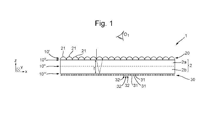
Hence, Figure 1 schematically depicts an embodiment of a security device 1, in
cross-section. The security device could be for example a moire magnifier, an
integral imaging device, a lenticular device or any other security device in
which
CA 03038874 2019-03-29
WO 2018/060726 PCT/GB2017/052928
27
an optically variable effect is generated by the co-operation between a
focussing
element array and an image array. The security device comprises a transparent
substrate 2, which is typically polymeric, and may be monolithic or formed of
multiple layers such as layers 2a, 2b in this example. Suitable polymeric
substrates include polypropylene (preferably BOPP), polyethylene,
polyvinylchloride and the like. The thickness of the substrate will be
selected
based on the desired end use. For instance if the security device is to be
formed
as a thread, strip, foil or other article for application to a security
document,
typically the substrate thickness will be 50 microns or less, more preferably
35
.. microns or less. In other cases, the substrate 2 could be a portion of a
document substrate such as that on which a polymer banknote is based in which
case the thickness will be greater, e.g. in the region of 70 to 200 microns.
A focussing element array 20 is provided on one surface of the substrate 2 and
comprises a regular array of focussing elements 21, such as lenses or mirrors.
The particular arrangement of focussing elements 21 will depend on the nature
of the optically variable effect to be generated. The array 20 may be periodic
in
one dimension or two dimensions ¨ Figure 1 depicts the array 20 as periodic in
the x-axis direction but it may additionally be periodic in the orthogonal y-
axis
direction. The individual focussing elements could comprise elongate elements
such as cylindrical focussing elements, or could be spherical or aspherical,
for
example. The focussing elements preferably take the form of lenses or mirrors.
In the Figure 1 embodiment, and in all the examples depicted below, the
focussing element array is exemplified as lenses but in all cases could be
replaced by a mirror array, in which case the observer 01 would view the
effect
from the opposite side of the device. The colour filter would need to be
repositioned within the structure accordingly.
The colour filter (generally denoted 10 in the Figures) may be integrated into
another component of the security device 1 or may be provided separately. For
instance, Figure 1 shows four exemplary locations for the colour filter 10,
labelled 10', 10", 10" and 101v. In a first preferred option, the colour
filter 10' is
incorporated into the focussing element array 20 by forming the focussing
CA 03038874 2019-03-29
WO 2018/060726 PCT/GB2017/052928
28
elements 21 of differently coloured transparent materials in different regions
of
the device. Hence the focussing elements themselves perform dual functions of
co-operating with the image array 30 to generate the optically variable effect
and
modifying the colour thereof. Alternatively, the colour filter 10" could be
located
between the focussing element array 20 and the surface of the substrate 2 on
which the focussing element array 20 is located, in the form of a pedestal
layer
(not shown separately in Figure 1). The pedestal layer will comprise
transparent
materials having different colours in different regions of the device 1.
If the substrate 2 is multi-layered, the colour filter 10" could alternatively
be
provided at some intermediate location within the substrate 2 at an internal
interface between adjacent substrate layers such as that illustrated between
layers 2a and 2b. In this case, the colour filter 10¨ could be a printed layer
of
coloured inks, for example. In a fourth example, the colour filter could be
located
between the image array 30 and the surface of the substrate on which the image
array is carried. Here the colour filter 101v could take the form of a printed
layer
on top of which the image array is then placed, or more preferable could be
formed as a multi-coloured tie coat of coloured curable materials, as will be
described further below.
For ease of manufacturing, colour filter locations 10" (pedestal layer) or
101v in
the form of a printed layer are especially preferred. However, forming the
colour
filter integrally with another component (e.g. in the focussing element array
or as
a tie coat) offers other advantages such as improved registration.
However the colour filter 10 is incorporated into the device, it comprises at
least
two transparent materials with different visibly coloured tints (one of which
may
be colourless), arranged in respective regions of the device. The colour
filter 10
modifies the observed colour of the underlying image array by transmitting
only
selected wavelengths of the visible spectrum therethrough, which are different
in
the different regions. To consider the effect of the colour filter 10 on the
appearance of the device, the following model is adopted:
CA 03038874 2019-03-29
WO 2018/060726 PCT/GB2017/052928
29
The visible spectrum can be represented by red, green and blue wavebands of
roughly equal width and therefore the terms R, G and B in the following
equations are just label indices.
We represent the reflected colour of the image elements or microimages 31
making up the image array as P(p) = (pr R, pg G, Pb B) or simply (Pr, pg ,
Pb).
Meanwhile, the reflected colour of the background 32 surrounding the image
elements of microimages is B(b)= (br R , bg G , bb B) or simply (br , bg ,
bb).
For example, for
Magenta: br, bb Pr , pb =1 and bg , pg = 0
Cyan: bb ,bg , Pb, pg = 1 and br , pr = 0
Yellow: br ,bg ,Pr ,pg ,1 and bb Pb, = 0
Black: br, bg ,bb ,Pr, pg Pb = 0
For the colour filter 10, the colour transmission is defined by T(t) = (tr R,
tg G, tb
B). For instance, a red filter as defined as that which passes only the red
wave
band and therefore t r = 1 and tg, tb = 0 etc.
Given the previous representation and notation, the observed background colour
exhibited by the image array 30 and colour filter 10 in combination can be
denoted OB = E, (b, = t,) i, whilst the observed colour of the image elements
or
microimages 31 is OP = E, (p, =t,) i.
To illustrate, suppose the background 32 is a pure cyan with the colour matrix
B(b) = (0,1,1) and the image elements 31 are magenta with the colour matrix
P(p) = (1,0,1). Suppose the colour filter 10 transmits 90% red, 5% green and
5% blue, then T = (0.9, 0.05, 0.05). Hence the observed background colour OB
will be (0, 0.05,0.05) i.e. very dark cyan, whilst the image element colour OP
will
be defined by (0.9, 0, 0.05) which will result in a bright red image element
31.
Thus the effect of the colour filter 10 here will be transform a "magenta on
cyan"
image array 30 to a "red on dark magenta" observed image array. We therefore
have a convenient way of qualitatively determining the observed colour for
more
CA 03038874 2019-03-29
WO 2018/060726 PCT/GB2017/052928
complex colour compositions present in background 32, image elements 31
and/or the colour filter 10.
Figure 2 shows these principles at work in an illustrative example. Here,
Figure
5 2(a) depicts an exemplary image array 30 which here comprises a regular
array
of microimages, each having in this example the form of the digit "5", which
are
formed in magenta, on a cyan background 32. Figure 2(b) shows an exemplary
colour filter 10 having three laterally offset and non-overlapping regions R1,
R2
and R3. In the first region R1, the colour filter is formed of a first
material 10a
10 having a red tint, in the second region R2, a second material 10b is
provided
which in this case is colourless (i.e. no tint), and in the third region R3 a
third
material 10c is provided which here has a green tint. Figure 2(c) shows the
colour filter 10 and image array 30 arranged to partially overlap one another.
Now, the image elements 31 which appear in the first region R1 are observed as
15 bright red against a dark cyan background, those appearing in the second
region
R2 are unmodified and hence are observed as magenta image elements 31
against a cyan background, and in the third region R3 the image elements 31
appear dark magenta on a green background. As a further example, if the
colour filter 10 was formed of a yellow tinted material 10b in second region
R2,
20 here the image elements 31 would appear red on a green background.
The above principles can be utilised to create various new and distinctive
effects
in optically variable security devices, of which preferred examples will now
be
described.
First, a comparative example of a lenticular device 10 is shown in Figure 3 in
order to illustrate certain principles of operation. Figure 3(a) shows the
device 1
in a perspective view and it will be seen that an array 20 of focussing
element
structures, here in the form of cylindrical lenses 21, is arranged on a
transparent
substrate 2. An image array 30 is provided on the opposite side of substrate 2
underlying (and overlapping with) the cylindrical lens array 20. Alternatively
the
image element array 30 could be located on the same surface of the substrate 2
as the lenses, directly under the lenses. Each cylindrical lens 21 has a
CA 03038874 2019-03-29
WO 2018/060726 PCT/GB2017/052928
31
corresponding optical footprint which is the area of the image element array
30
which can be viewed via the corresponding lens 21. In this example, the image
array 30 is an interlaced image array comprising a series of image slices, of
which two slices 31, 32 are provided in (and fill) each optical footprint.
The image slices 31 each correspond to strips taken from a first image IA
whilst
the image slices 32 each correspond to strips of a second image IB. Thus, the
size and shape of each first image slice 31 is substantially identical (being
elongate and of width equal to half the optical footprint), but their
information
content will likely differ from one first image slice 31 to the next (unless
the first
image IA is a uniform, solid colour block). The same applies to the second
image
slices 32. The overall pattern of image slices is a line pattern, the elongate
direction of the lines lying substantially parallel to the axial direction of
the
focussing elements 21, which here is along the y-axis. The lenses 21 and the
image slices 31, 32 are periodic in the orthogonal direction (x-axis) which
may
be referred to below as the first direction of the device.
As shown best in the cross-section of Figure 3(b), the image element array 30
and the focussing element array have substantially the same periodicity as one
another in the x-axis direction, such that one first image slice 31 and one
second
image slice 32 lies under each lens 21. The pitch S of the lens array 20 and
of
the image element array 30 is substantially equal and is constant across the
whole device. In this example, the image array 30 is registered to the lens
array
20 in the x-axis direction (i.e. in the arrays' direction of periodicity) such
that a
first pattern element 31 lies under the left half of each lens and a second
pattern
element 32 lies under the right half. However, registration between the lens
array 20 and the image array 30 in the periodic dimension is not essential.
When the device is viewed by a first observer 01 from a first viewing angle,
as
shown in Figure 3(b) each lens 21 will direct light from the underlying first
image
slice 31 to the observer, with the result that the device as a whole appears
to
display the appearance of the first image IA, which in this case is a uniform
block
colour as shown in in Figure 1(c). The full image IA is reconstructed by the
CA 03038874 2019-03-29
WO 2018/060726 PCT/GB2017/052928
32
observer 01 from the first image slices 31 directed to him by the lens array
20.
When the device is tilted so that it is viewed by second observer 02 from a
second viewing angle, now each lens 21 directs light from the second image
slices 32 to the observer. As such the whole device will now appear to display
a
second image IB, which in this example is blank, as shown in Figure 1(c),
although it could comprise any alternative image. Hence, as the security
device
is tilted back and forth between the positions of observer 01 and observer 02,
the appearance of the whole device switches between image IA and image IB.
In this example the first image elements 31 are provided by material forming
the
image array 30 whilst the second image elements 32 are provided by gaps
therebetween. However in other cases as illustrated below the second image
elements 32 could also be coloured, e.g. by providing a coloured background
such as that described with reference to Figure 2 above. It is also possible
to
interleave three of more images by extending the above principles accordingly.
As also noted in passing, the images need not be uniform blocks of colour (or
lack thereof) but could each carry any desirable graphic, such as indicia or
the
like, by arranging each image slice 31 to be provided only in accordance with
the
desired graphic rather than in a continuous form along its length, as shown.
Figure 4 illustrates an embodiment of a security device 1 in accordance with
an
aspect of the present invention which here is a lenticular device operating on
the
same principles described with respect to Figure 3. Components of the device 1
are labelled using like reference numerals as before and so those already
introduced will not be described again. The security device 1 comprises two
laterally offset regions R1 and R2 which, as shown best in the plan views of
Figures 4(b) and (c) are arranged as a circular area R2 on a rectangular
surroundings R1. The device incorporates a colour filter 10 of the type
described
above which here is incorporated into the focussing element array 20, but
could
take any of the other implementations already mentioned. However in this
example, the focussing elements 21a in the first region R1 are formed of a
transparent material in a first colour (e.g. blue) whilst the focussing
elements 21b
in the second region R2 have a second colour (e.g. yellow). The image array 30
CA 03038874 2019-03-29
WO 2018/060726 PCT/GB2017/052928
33
once again comprises first image slices 31 spaced by background slices 32
arranged so as to generate the above-described lenticular switching effect in
combination with the focussing elements 21, upon tilting of the device.
However,
in the second region R2, the image array is laterally shifted in the x-axis
direction
.. relative to its translational position in the first region R1 (i.e. "phase-
shifted"),
which can be achieved through design of the image array 30. Thus, in the first
region R1 the first image slices 31 sit under the left half of each focussing
element 21 whilst the second image slices 32 occupy the right half, and in the
second region R the arrangement is reversed. In this example, the first image
slices 31 are achromatic (e.g. black) whilst the second image slices 32 are
colourless.
Figures 4(b) and (c) show the appearance of the device from two different
viewing angles for respective observers 01 and 02. Observer 01 sees outer
region R1 appearing dark blue/black due to the combination of the blue lenses
21a with the black image elements 31. However in the central region R2 the
focussing elements 21 will direct light from the second image elements 32 to
the
same observer 01, due to the phase-shifted image array 30 and this in
combination with the yellow lenses 21b will cause the region R2 to appear
bright
yellow. When the device is tilted and viewed by observer 02, now in the outer
region R1, the blue lenses 21a will direct light from the second image slices
32 to
the viewer causing that region to appear bright blue whilst the central region
R2
will now appear dark yellow or gold due to the combination of the yellow
lenses
21b and dark image elements 31. Hence, overall two different colours, each at
two different darkness levels, are displayed by the device over the full range
of
viewing angles. In addition it will be noted that the contrast between the two
regions has reversed during tilting: observer 01 sees the outer region R1 as
dark
compared with the centre region R2 whereas the reverse is true for observer
02.
This provides a particularly strong and distinctive visual effect.
By requiring both the colour filter 10 and the image array 30 to possess
different
characteristics in respective regions of the device 1, the device presents a
significant challenge to would-be counterfeiters, since any mis-registration
CA 03038874 2019-03-29
WO 2018/060726 PCT/GB2017/052928
34
between the colour filter 10 and the image array 30 will be noticeable since
additional colour effects will appear at the boundaries between regions.
Figure 5 illustrates another embodiment of a security device 1 which is a
variant
of that depicted in Figure 4 and operates on the same principles. Here, the
two
regions R1, R2 are laterally offset rectangular areas of the device 1 and once
again the colours of the colour filter 10 and the translational position of
the image
array 30 are varied between regions. In this example, however, the image
elements 31 are not achromatic but themselves carry a hue which when
combined with colours of the colour filter creates additional effects. To
illustrate
this, here the colour filter 10 (incorporated again into the focussing element
array
20) is colourless in the first region R1 but carries a yellow tint in the
second
region R2. The image elements 31 are blue and the gaps 32 between them are
colourless. Now, observer 01 sees the first region R1 as light blue and the
second region R2 as yellow. Upon tilting, observer 02 sees the first region R1
as
colourless and the second region R2 as green (due to the combination of blue
and yellow). Hence four different colours are visible across the whole range
of
viewing angles, despite only three having been used in its production
(counting
colourless).
In the Figure 6 embodiment, new colour effects are achieved by matching at
least one of the colours in the colour filter 10 to at least one colour of the
image
array 30. Again the construction is similar to that in the two preceding
embodiments and so only the differences will be highlighted here. The image
array 30 in this example is formed of yellow first image slices 31 and
intervening
blue second image slices 32. Unlike in the preceding embodiments, there is no
phase-shift in the image array 30 between regions and the arrangement of
image slices continues uniformly across the device 1. The colour filter 10,
meanwhile, is blue in the first region R1 and yellow in the second region R2
such
that in this example the two colours in the filter 10 match each of the two
colours
in the image array 30 (although this is not essential, only one matching
colours is
required).
CA 03038874 2019-03-29
WO 2018/060726 PCT/GB2017/052928
The described arrangement results in the generation of a new third colour
which
appears to move between regions upon tilting of the device. As shown in
Figures 6(b) and (c), the first observer 01 sees the first region R1 as green
due
to the combination of the blue lenses 21a and the yellow first image slices
31,
5 and the second region R2 as yellow. Upon tilting, observer 02 now sees
the first
region R1 as blue whilst the new green colour has moved to the second region
R2.
Another effect can be achieved by adding a phase-shift to the image array 30
10 between regions, as illustrated in the embodiment of Figure 7. Here the
construction of the device and choice of colours is the same as in the Figure
6
embodiment, the only difference being that the image slices have been
laterally
shifted in region R2 relative to region R1. Now, observer 01 will perceive
both
regions R1 and R2 as green, whereas observer 02 will see only the two original
15 colours: blue in region R1 and yellow in region R2. Hence the third
colour, green,
appears and disappears as the device is tilted.
The above examples of security devices have all operated on lenticular
principles but colour filters of the types just mentioned in which at least
one of
20 .. the colour filter regions matches a colour in the image array also have
particular
benefit in security devices such as moire magnifiers and integral imaging
devices.
To illustrate the principles of operation, comparative examples of moire
magnifier
25 .. and integral imaging devices will first be described with reference to
Figures 8
and 9 respectively.
Figure 8 depicts an exemplary moire magnifier device, comprising an image
element array 30 defining an array of microimages 31 and an overlapping
30 focussing element array 20 with a pitch or rotational mismatch as
necessary to
achieve the moire effect. Figure 8(a) depicts part of the image element array
30
as it would appear without the overlapping focusing element array, i.e. the
non-
magnified microimage array (but shown at a greatly increased scale for
clarity).
CA 03038874 2019-03-29
WO 2018/060726 PCT/GB2017/052928
36
In contrast, Figure 8(b) depicts the appearance of the same portion of the
completed security device, i.e. the magnified microimages 34, seen when
viewed with the overlapping focussing element array, at one viewing angle. It
will be seen from Figure 8(a) that the image array 30 here forms a regular
array
of microimages 31 which here each convey the digit "5". In this case all of
the
microimages 31 are of identical shape and size. The microimages 31 may be
coloured or achromatic, formed of ink for example.
Surrounding the
microimages 31 is a contiguous, uniform background 32 which is preferably
colourless but could be of a second contrasting colour. Alternatively, the
arrangement could be reversed with the microimages 31 formed as negative,
colourless gaps in a coloured background 32.
Figure 8(b) shows the completed security device 1, i.e. the image element
array
30 shown in Figure 8(a) plus an overlapping focusing element array 20, from a
first viewing angle which here is approximately normal to the plane of the
device
30. It should be noted that the security device is depicted at the same scale
as
used in Figure 8(a): the apparent enlargement is the effect of the focusing
element array 20 now included. The moire effect acts to magnify the
microimage array such that magnified versions 34 of the microimages 31 are
displayed. In this example just two of the magnified microimages are shown. In
practice, the size of the enlarged images and their orientation relative to
the
device will depend on the degree of mismatch between the focussing element
array. This will be fixed once the focusing element array is joined to the
image
element array. The magnified microimages will appear to move laterally
relative
to the device upon tilting and depending on the magnification level may be
visualised above or below the surface plane of the device 1.
In the above example security device, the microimages are all identical to one
another, such that the devices can be considered "pure" moire magnifiers.
However, the same principles can be applied to "hybrid" moire magnifier /
integral imaging devices, in which the microimages depict an object or scene
from different viewpoints. Such microimages are considered substantially
identical to one another for the purposes of the present invention. An example
CA 03038874 2019-03-29
WO 2018/060726 PCT/GB2017/052928
37
of such a device is shown schematically in Figure 9, where Figure 9(a) shows
the unmagnified microimage array, without the effect of focusing elements 21,
and Figure 9(b) shows the appearance of the finished device, i.e. the
magnified
image. As shown in Figure 9(a), the microimages 31 show an object, here a
cube, from different angles. It should be noted that the microimages are
formed
as lines of one colour corresponding to the black lines of the cubes in the
Figure,
the remainder of the image array 30 providing a background thereto which may
be coloured or contrasting. Again this arrangement could be reversed with the
lines formed as colourless gaps in a coloured background layer. In the
magnified image (Figure 9(b)), the moire effect generates magnified, 3D
versions of the cube labelled 34. As the device is tilted the magnified cubes
34
will appear to move across the device, amounting to an effect with significant
visual impact.
Figure 10 shows another embodiment of a security device 1 in accordance with
an aspect of the invention, which here is a moire magnifier or integral
imaging
device. Thus whilst the physical structure of the device 1 is much the same as
that described in the preceding embodiments, here the image array 30
comprises a regular array of microimages 31 rather than image slices. The
microimages are arranged with a pitch mismatch and/or a rotational mismatch
relative to the focussing element array 20 such that the device as a whole
exhibits magnified versions of the microimages 31 as described with reference
to
Figures 8 and 9 above. The focussing element array could possess one
dimensional or two dimensional periodicity, e.g. being formed of cylindrical,
spherical or aspherical lenses. In a first region R1 of the device, the
focussing
elements 21a carry a coloured tint, e.g. yellow, whereas in a second region of
the device R2, the focussing elements 21b are colourless (although could
possess any other colour different to that in region R1). The image array 30
comprises microimages 31 which substantially match the colour of the filter 10
in
region R1 and hence are yellow in this example, against a colourless
background
(e.g. white, silver-reflective or clear).
CA 03038874 2019-03-29
WO 2018/060726 PCT/GB2017/052928
38
As seen in the plan view of Figure 10(b), the central second region R2 here
has
the shape of a star whilst the first region R1 provides a background thereto
filling
the remainder of the rectangular device area.
In the central second region R2, the focussing elements 21b will cooperate
with
the microimages 31 in a standard manner to exhibit the desired optically
variable
effect. In the surrounding first region R1, however, the matching colours of
the
filter 10 and the microimages 31, together with the colourless background 32,
reduce or preferably prevent the visualisation of the microimages such that
the
appearance of the optically variable effect is substantially diminished and
preferably eliminated. As a result, the device 1 appears optically variable
only
across star-shaped region R2 and not elsewhere. This approach enables the
shape, size and position of the optically variable area to be controlled
solely
through design of the colour filter 10 whilst the image array 30 can be
provided
in a continuous manner without modification. As such, more complex device
designs can be achieved.
The embodiment shown in Figure 11 advances the same principles a step
further by making use of two image arrays 30a and 30b. The construction of the
.. device 1 is otherwise the same as in the Figure 10 example and so will not
be
described again here. The two image arrays 30a and 30b are formed in different
colours from one another: hence, in an example the image array 30a is yellow
(as per image array 30 in the preceding embodiment) whilst image array 30b is
blue. Both image arrays have colourless backgrounds 32. Both of the image
arrays may be provided across the whole area of the device, overlapping one
another, e.g. formed in two sequential printed workings. The image arrays 30a
and 30b might each define an array of microimages 31a, 31b which co-operates
with the focussing element array 20 to exhibit a moire magnification or
integral
imaging effect, or they could each be designed to generate different effects
in
combination with the focussing elements such as a moire magnification effect
from image array 30a and a lenticular effect from image array 30b. In this
example, each image array 30a, 30b is adapted to generate a moire
magnification effect in combination with the focussing elements 20.
CA 03038874 2019-03-29
WO 2018/060726 PCT/GB2017/052928
39
In the first region R1, forming the outer surroundings of the device 1, as in
the
previous example, the optically variable effect from image array 30a is
inhibited
due to the colour matching between the colour filter 10 and the microimages
31a. However, the microimages 31b of the second image array 30b will not be
inhibited since here the colours do not match. Thus, the optically variable
effect
arising from the second image array 30b (only) will be exhibited in the first
region
R1. In the second region R2 which again has here the shape of a star, since
the
colour filter 10 is colourless neither of the image arrays 30a, 30b will be
inhibited
and hence both optically variable effects will be displayed, superimposed on
one
another. The two image arrays can be designed to make best use of this
superposition, e.g. through selection of the microimage content ¨ for instance
the microimages 31a could each be "" signs and the microimages 31b each the
digit "10" so that in combination information concerning the denomination
"10"
is conveyed ¨ and/or by configuring each set of magnified images to be
visualised at different apparent heights or depths ¨ for instance one set
could
appear to float above the device and the other appear sunken below it.
Alternatively, the colours could be selected so that each region of the colour
filter
.. matches one of the colours of the image arrays 30. This can be used to
select
single ones of the image arrays 30a, 30b etc to be active in each region. For
instance if the Figure 11 embodiment where modified such that the colour filer
10 is blue in region R2, now only the optically variable effect generated by
the
first image array 30a will be exhibited in that region, whilst that generated
by the
second image array 30b will be inhibited due to the matching colours.
Generally, the colour of the colour filter 10 can therefore be used, by
applying
the principles above, to select which of a plurality of image arrays 30 is
visualised in each region of the device. Any number of differently coloured
image arrays 30 and regions could be combined in this way across the device,
resulting in a highly complex appearance which is very difficult to replicate.
CA 03038874 2019-03-29
WO 2018/060726 PCT/GB2017/052928
In some of the above embodiments, the distinctive visual effects are achieved
by
matching a colour of the colour filter 10 to a colour of the image array 30.
However, other strong effects can be achieved by arranging a colour of the
colour filter 10 to be complementary to a colour of the image array 30. A
5 complementary colour is one which if mixed with its corresponding colour
would
provide substantially all wavelengths of the visible spectrum and so appear
either black or white depending on whether the colour mixing mechanism is
additive or subtractive. By utilising complementary colours in this way, the
contrast between the various colours exhibited by the device (either between a
10 microimage and its surroundings viewed simultaneously, or between
different
images in a lenticular device) can be enhanced and hence the effect made more
visually distinct.
Figures 12 and 13 show two examples of security devices 1 utilising this
15 principle which otherwise largely correspond in structure to the
embodiments
shown in Figures 6 and 7 respectively. Hence, only the modifications to those
previous embodiments will now be described. In both examples, the security
devices 1 are lenticular devices.
20 In the Figure 12 embodiment, the colour filter 10 is arranged to be cyan
in region
R1 and yellow in region R2, whilst image elements 31 of array 30 are red,
spaced
by colourless gaps 32. Red and cyan are complementary colours according to
the RGB additive colour model and the CMY subtractive colour model.
25 When viewed from a first viewing angle, observer 01 perceives the first
region R1
to be very dark blue/indigo due to the combination of the cyan lenses 21a with
the red image elements 31. The second region R2 appears orange. Upon tilting
to another viewing angle, the second observer 02 sees the first region R1 as
light
blue and the second region R2 as yellow. Hence four different colours are
30 visualised.
The Figure 13 embodiment is substantially the same as the Figure 12
embodiment except that here an additional effect is introduced by phase-
shifting
CA 03038874 2019-03-29
WO 2018/060726 PCT/GB2017/052928
41
the image array 30 between regions as in the earlier embodiments described
herein. Thus, observer 01 again perceives the first region R1 to be very dark
blue/indigo but now the second region R2 appears yellow. Upon tilting to
another viewing angle, the second observer 02 sees the first region R1 as
light
blue and the second region R2 as orange. Hence the position of the darker
contrast region appears to move upon tilting.
In the preceding embodiments, the colour effects are achieved by the
combination of the image array 30 and the overlying colour filter 10. However,
still more complex effects can be achieved by additionally providing a multi-
coloured backing layer which sits on the opposite side of the image array 30
and
provides colour to any gaps therein between the image elements 31. Figures 14
to 17 provide four examples of embodiments of security devices making use of
such a backing layer 40.
For ease of comparison, the embodiments of Figures 14 and 15 correspond in
all respects other than the provision of the backing layer 40 to the
embodiments
just described with reference to Figures 12 and 13, respectively. However it
should be appreciated that here it is not essential for the image array 30 to
be
provided in a colour which is complementary to either of the colours of the
colour
filter 10, although this is preferred in order to provide enhanced contrast as
mentioned above.
Hence, the backing layer 40 can be provided as a printed layer or the like
which
covers at least part of the image array 30 on the side opposite from that on
which the viewer is located in use. The backing layer 40 comprises at least
two
differently coloured materials 41a, 41b arranged in respective areas of the
layer.
It should be noted that these areas need not correspond to the aforementioned
regions of the device, but this is preferred and in this example the first
area of
the backing layer containing material 41a corresponds to the first region R1
whilst the second area of the backing layer containing material 41b
corresponds
to the second region R2. The colours of the backing layer could be different
to
those of the colour filter but in this example they are the same. Hence, in
region
CA 03038874 2019-03-29
WO 2018/060726 PCT/GB2017/052928
42
R1 the focussing elements 21a are cyan as is the backing material 41a, and in
region R2, the focussing elements 21b and the backing material 41b are both
yellow. The image elements 31 are red, spaced by colourless gaps 32.
When viewed from a first viewing angle, observer 01 perceives the first region
R1
to be very dark blue/indigo due to the combination of the cyan lenses 21a with
the red image elements 31. The second region R2 appears orange. These
colours are the same as in the Figure 12 embodiment since the backing layer
does not contribute here due to masking by the image elements 31. Upon tilting
to another viewing angle, the second observer 02 sees now the first region R1
as
bright blue and the second region R2 as bright yellow, each with increased
colour intensity due to the contributions from the colour filter 10 and
backing
layer 40.
Similarly, the Figure 15 embodiment is identical to the Figure 14 embodiment,
save for phase-shifting of the image array 30 between the two regions. Thus,
observer 01 again perceives the first region R1 to be very dark blue/indigo
but
now the second region R2 appears bright yellow. Upon tilting to another
viewing
angle, the second observer 02 sees the first region R1 as bright blue and the
.. second region R2 as orange. Hence the position of the darker contrast
region
appears to move upon tilting.
The complexity of the appearance can be further increased by arranging the
areas of the backing layer 40 to differ from the regions R1, R2. For instance,
multiple areas of the backing layer 40 could be located within any one of the
regions. This is the case in the embodiments of Figures 16 and 17 which are
otherwise structurally the same as the embodiments of Figures 14 and 15
respectively. Here, the backing layer 40 comprises four regions with materials
41a and 41b occupying the two halves of first region R1 and materials 41c and
41d occupying the two halves of second region R2. Materials 41a and 41c are
cyan whilst materials 41b and 41d are yellow. The colour filter 10 is once
again
cyan in region R1 and yellow in region R2, whilst the image elements 31 are
red.
CA 03038874 2019-03-29
WO 2018/060726 PCT/GB2017/052928
43
When the device is viewed at a first angle by observer 01, the whole of region
R1
appears dark blue / indigo since once again the backing layer 40 does not
contribute, and similarly the second region R2 appears orange. However upon
tilting the arrangement of differently colours portions changes: now only half
of
region R1 appears light blue (corresponding to area 41a of the backing layer)
whilst the other half and the neighbouring half of the second region R2
(corresponding to areas 41b and c) appear green, and the last half of region
r2
appears yellow (area 41d). Hence five different colours are exhibited across
the
range of viewing angles, and the pattern of differently coloured device
portions
also changes.
The Figure 17 embodiment is identical to the Figure 16 embodiment, save for
phase-shifting of the image array 30 between the two regions. Thus, observer
01
again perceives the first region R1 to be very dark blue/indigo but now the
second region R2 appears in two halves: green in area 41c and yellow in area
41d. Upon tilting, observer 02 now sees the first region R1 split into two
halves
41a, 41b which are bright blue and green respectively while the whole of
region
R2 is orange.
In all of the embodiments described so far the colour filter 10 has been
formed
integrally with the focussing elements array 20, e.g. in the form of coloured
lenses. Preferred methods for forming multi-coloured focussing element arrays
suitable for this purpose will now be described with reference to Figures 18,
19
and 20, and are disclosed in more detail in our existing International patent
application no. PCT/GB2016/052082.
In embodiments of the present invention, the focussing element array 20 is
formed by cast-curing. This involves applying one or more transparent curable
material either to the support layer or to a casting tool carrying a surface
relief
defining the desired focussing element array, forming the material using the
casting tool and curing the material to fix the relief structure into the
surface of
the material.
CA 03038874 2019-03-29
WO 2018/060726 PCT/GB2017/052928
44
Referring to Figure 18, a first transparent curable material 205a is applied
to a
support layer 201 (such as the substrate 2 shown in previous embodiments)
using an application module 210a which here comprises a patterned print
cylinder 211a which is supplied with the curable material from a doctor
chamber
213a via an intermediate roller 212a. For example, the components shown
could form part of a gravure printing system. Other printing techniques such
as
lithographic, flexographic, screen printing or offset printing could also be
used.
Print processes such as these are preferred since the curable material 205a
can
then be laid down on the support 201 only in first regions 202a thereof, the
size,
shape and location of which can be selected by control of the print process,
e.g.
through appropriate configuration of the pattern on cylinder 211a. The curable
material 205a is applied to the support 201 in an uncured (or at least not
fully
cured) state and therefore may be fluid or a formable solid.
A second application module 201b is then used to apply a second transparent
curable material 205b to other second regions 202b of the support layer 201.
The second application module is typically of the same construction as the
first.
The second transparent material 205b will have a different optical detection
characteristic, particularly its visible colour, from the first material 205a.
The support 201 is then conveyed to a casting module 220 which here
comprises a casting tool 221 in the form of a cylinder carrying a surface
relief
225 defining the shape of the focussing elements which are to be cast into the
curable materials 205a,b. As each patch 202 (comprising regions 202a and
202b) of curable material 205 (comprising materials 205a and 205b) comes into
contact with the cylinder 221, the curable material 205 fills a corresponding
region of the relief structure, forming the surface of the curable material
into the
shape defined by the relief. The cylinder 221 could be configured such that
the
relief structure 225 is only provided at regions corresponding to shape and
position of the patches 202 of curable material 205. However this gives rise
to
the need for accurate registration between the application module 210 and the
casting module 220 in order that the focussing elements are accurately placed
in
each first region 202 of the curable material. Therefore in a particularly
preferred
CA 03038874 2019-03-29
WO 2018/060726 PCT/GB2017/052928
example, the cylinder 221 carries the relief structure corresponding to the
focussing elements over an area larger than that of the patch 202, preferably
around its complete circumference and most preferably over substantially its
whole surface (although axial regions which will not come into the vicinity of
the
5 curable material may be excluded). In this way, each entire patch 202 of
curable
material 205 is guaranteed to come into contact with the surface relief
structure
225 such that the focussing element array is formed over the full extent of
the
material. As a result, the shape, size and location of the focussing element
array
20 is determined solely by the application of the curable material by the
10 application modules.
Having been formed into the correct surface relief structure, the curable
material
205 is cured by exposing it to appropriate curing energy such as radiation R
from
a source 222. This preferably takes place while the curable material is in
contact
15 with the surface relief 225 although if the material is already
sufficiently viscous
this could be performed after separation. In the example shown, the material
is
irradiated through the support layer 201 although the source 222 could
alternatively be positioned above the support layer 201, e.g. inside cylinder
221
if the cylinder is formed from a suitable transparent material such as quartz.
The surface relief 225 may be carried by cylinder 221 in the form of a sheet
embossed or otherwise provided with the required relief, which is wrapped
around the cylinder 221 and clamped in place. This may result in a noticeable
join 225a where the two ends of the sheet meet, at which there is a
discrepancy
in the relief pattern. If replicated into one of the focussing element arrays
this
would cause a reduction in quality. It is therefore preferred that the casting
module is at least coarsely registered to the application module so that the
location of join 225a where it contacts support 201 does not coincide with any
of
the first regions 202 but rather is located between them, as shown by the
example location labelled 225b. In cases where the curable material is applied
(and retained) all over the support, or at least along a continuous strip in
the
machine direction MD, this join 225a is still preferably positioned outside
the first
region which is to be used to form the security device, advantageously in a
CA 03038874 2019-03-29
WO 2018/060726 PCT/GB2017/052928
46
location which will subsequently be coated with one of the opacifying layers
3.
To achieve this consistently it is desirable for the process for forming the
focussing element array to be registered with the opacifying layer application
process, e.g. performed in the same in-line process.
It will be noted that in the present example the two regions 202a, 202b (which
correspond to regions R1, R2 in the preceding embodiments abut one another,
as is preferred. Either the perimeter of the first region 202 as a whole,
and/or
the two regions 202a,b (in combination or independently of one another)
preferably define indicia. The two application modules 210a,b are preferably
registered to one another, e.g. performed in the same in-line process. The two
curable materials 205a,b are then brought into contact with the casting
cylinder
221 so as to form the surface relief into both materials, and cured as
previously
described. The result is a focussing element array formed of at least two
materials laterally offset from one another (i.e. side by side), giving rise
to an
optically detectable pattern or indicia.
Figures 19 and 20 show two alternative apparatus arrangements which may be
used to form focussing element arrays of at least two materials. In these
examples, the two curable materials 205a,b are applied to the casting cylinder
221' rather than to the support layer 201. Thus, in the Figure 19 embodiment,
application module 210a selectively applies a first curable material 205a to
first
regions 202a of the surface relief 225 on cylinder 221' and then application
module 210b selectively applies a second curable material 205b to second
regions 202b. In each application module 210, either or both of the rollers
211,
212 in the inking chain may be patterned. For example, rollers 212a,b may be
pattered gravure rollers configured to take up resin on selected portions of
their
surfaces only, with respective removal means 213a', 213b' such as doctor
blades optionally being provided to remove any excess. Rollers 211a,b may
then be uniform transfer rollers. The patterning required to form patches 202
and regions 202a, 202b could be achieved solely by the two application modules
210a,b in which case the focussing element relief structure 225 may be
provided
continuously across the whole surface of casting cylinder 221'. Alternatively,
as
CA 03038874 2019-03-29
WO 2018/060726 PCT/GB2017/052928
47
shown in Figure 19, the relief structure 225 may be provided only in discrete
patches on the surface of cylinder 221' and an optional removal means 213a",
213b" such as respective doctor blades can be provided after each application
station to remove any excess material. The precise location and extent of the
patches 202 (and the regions thereof) which are ultimately formed on the
support layer 201 may be determined by the manner in which the curable
materials 205a,b and/or by the arrangement of the surface relief structure 225
on
the cylinder 221'.
In a variant, shown in Figure 20, rather than apply the two curable materials
205a,b onto the support layer 201 sequentially, the two application modules
could be configured to apply the respective curable materials in the desired
pattern onto some intermediate component, such as a blanket or an offset
roller.
The pattern of different curable materials can then be transferred onto the
.. support layer 201 in a single application step. This has been found to
improve
the achievable registration. Thus, the apparatus shown in Figure 20
corresponds largely to that of Figure 19 except for the provision of collect
roller
214 which is inserted between the application modules 210a, 210b and the
casting cylinder 221'. Thus, each application module 210a,b deposits its
curable
.. material 205a,b in a pattern onto the surface of collect roller 214, from
which
both materials 205a,b are then transferred together onto the casting cylinder
221'. This approach has been found to achieve particularly accurate
registration
between the two curable materials 205a,b.
As mentioned at the outset, the colour layer could alternatively be provided
at
various different locations within the security device structure, and this
applies to
all embodiments described above. For example, the security device could be
constructed utilising a lens array (or other focussing element array) formed
as a
transfer element which is then affixed to a substrate carrying the image array
on
its opposite side. The substrate could be that of a polymer banknote, for
example. Figure 21a shows a cross-section through an exemplary lens transfer
structure 50 formed using methods disclosed in our British patent application
no.
1607480.9. The lens transfer structure 50 comprises a layer of carrier
material
CA 03038874 2019-03-29
WO 2018/060726 PCT/GB2017/052928
48
51, an upper surface of which has preferably been corona treated. On the upper
surface of the carrier material is a layer of first material 52, which is
substantially
transparent, and has a first refractive index, of 1.35 for example. The upper
surface of the first material 52 is shaped into a lens relief structure, which
in this
embodiment is a regular two-dimensional array of concavities suitable for
functioning as a two-dimensional array of spherical lenses. Over the lens
relief
structure, i.e. over and in contact with the upper surface of the first
material 52,
is located a layer of second material 53, a lower surface of which conforms to
the lens relief structure, and an upper surface of which is spaced from the
lens
relief structure and is substantially flat. The second material is also
substantially
transparent, and has a second, different refractive index, of 1.55 for
example.
The refractive index of the second material 26 is higher than that of the
first
material 21 such that the second material filling the concavities in the
surface of
the first material acts as an array of spherical, convex lenses, in this
example.
The transfer structure 50 is also provided with an adhesive layer 54 for
affixing
the lens structure to a substrate, although this adhesive layer could
alternatively
be provided on the substrate itself. The adhesive 54 is preferably heat-
activated
so that portions of the transfer element can be transferred to the substrate
by hot
stamping for example. In this embodiment, the adhesive layer 54 provides the
colour filter 10. Hence, different portions of the adhesive layer 54 are
differently
coloured. In this example, two differently coloured regions 54a and 54b are
shown to illustrate this.
Figure 21b shows the lens structure 50 described above having been transferred
onto a security article, in this case a security document, however it could
equally
be transferred to any substrate, for example a security element such as a
security thread.. Transfer of the lens structure may be achieved by placing
the
upper surface of the lens transfer structure, i.e. the substantially flat
surface of
the second material 53 or the adhesive layer 54 if this is present, in contact
with
a surface of a substrate 2 of a security document (if the adhesive layer 54 is
not
provided as part of the transfer element 50 this will be pre-applied to the
surface
of substrate 2). The carrier layer 51 is then peeled away from the lens
structure,
leaving the lens structure formed by layers of the first and second material
52
CA 03038874 2019-03-29
WO 2018/060726 PCT/GB2017/052928
49
and 53, and adhesive layer 54, on the surface of the substrate. The carrier
layer
is removed substantially without distorting the lens array provided within the
lens
structure since the peel strength of the bond between the carrier layer 51 and
the first material 52 is relatively low, and in particular, is lower than the
peel
strength of the bond between the first and second materials 52 and 53.
Figure 21b shows the lens structure on a transparent substrate 2, which may
for
example be a polymer, such as biaxially oriented polypropylene (BOPP) as used
in polymer banknotes. On a surface of the substrate 2 opposite to the lens
.. structure is located image array 30. As previously described, the colour
filter
layer 54 will act to modify the appearance of the image array 30 and hence of
the optically variable effect ultimately generated by the device.
In a variant of this embodiment, rather than colour the adhesive layer 54, a
.. colour filter layer may be applied between layers 53 and 54 or printed onto
the
surface of substrate 2 before the lens transfer structure 50 is applied.
Figure 22a schematically shows a further embodiment in which the colour filter
10 is provided in the form of a multi-coloured pedestal layer 25 located under
the
focussing element array on the surface of substrate 2, which is colourless (or
of
a single uniform colour) across the device. In this example the device has
three
concentric regions R1, R2 and R3 in each of which the pedestal layer is formed
by
a differently coloured transparent material 25a, 25b, 25c. Pedestal layers are
described in more detail in our existing International Patent Application No.
PCT/GB2016/052085 and typically have a preferred height in the region of at
least 1 micron, more preferably at least 3 microns and most preferably at
least 5
microns. The pedestal materials 10a,b,c are preferably flexible elastomers
which helps improve the resilience of the device 1.
A preferred method for forming a focussing element array with a pedestal layer
will now be discussed with reference to Figure 22b. Again, this involves cast-
curing and any of the method variants described above could be employed for
application of the curable material(s) 205 and forming thereof. However, an
CA 03038874 2019-03-29
WO 2018/060726 PCT/GB2017/052928
additional layer, referred to as a pedestal layer 25, is formed between the
curable material(s) in which the focussing element array is defined and the
support layer 201.
5 Thus Figure 22b shows an exemplary process in which, prior to application
of
the curable material 205 to the support layer 201, a pedestal layer 25 is
formed
by applying at least two transparent materials 207a,b to the support layer
201,
using pedestal application modules 240a,b. Again this could involve printing
or
coating the transparent materials 207a,b onto the support layer using any of
the
10 same methods as previous mentioned for the application of curable
material
205, such as gravure printing. In this example the material 207a is applied to
a
patterned gravure roller 241a from a reservoir 243a and a removal means 243a'
such as a doctor blade is provided for removing any excess material. If
necessary, the support layer is then conveyed through a drying and/or curing
15 section 245a to fix the material 207a. Whether the section 245a involves
drying
and/or curing will depend on the nature of the material 208a. Next the support
layer 201 is conveyed through a second pedestal application module 240b at
which a section transparent material 207b, of different colour, is applied
selectively to a second region 208b of the support layer 201, in register with
the
20 first material 207a. The apparatus of the second pedestal application
module
240b corresponds to that of the first pedestal application module 240a in this
example. Again, a drying and/or curing section 245b may be provided for fixing
the second material 207b. The pedestal materials 207a,b do need to cover at
least the patches 202 in which the focussing element arrays are to be formed.
In
25 the example depicted, the areas 208a,b to which the pedestal materials
207a,b
are applied are coincident with the patches 202, but this is not essential,
and
indeed may not be desirable since this gives rise to greater registration
requirements. In more preferred examples, the each pair of regions 208a,b to
which the pedestal materials 207a,b are applied are collectively larger than
the
30 extent of the respective focussing element array to be formed thereon,
at least in
the machine direction MD. This reduces the accuracy with which the lens
application and formation stage must be registered to the pedestal application
stage.
CA 03038874 2019-03-29
WO 2018/060726 PCT/GB2017/052928
51
The transparent materials 207a,b forming the pedestal layer may or may not
also be a curable material. If not, the transparent material is preferably
dried or
otherwise solidified sufficiently before proceeding. If the material is
curable, it
may be cured during application from cylinder 241a,b or after, possibly at the
same time as curing the curable material 205. However, preferably at least
partial curing of material 207a,b takes place before curable material 205 is
applied, which takes place at application station 210. In this example, this
comprises a patterned gravure cylinder 211 onto which the curable material 205
.. is applied from a reservoir 213, a doctor blade 213' or similar being
provided to
remove excess. The curable material 205 can be applied in the same way as
previously described but now is applied onto the pedestal layer 25 rather than
onto the support layer 201. The curable material is then brought into contact
with the casting tool 221 at casting station 220 in the same manner as
previously
described, and the focussing element array formed and cured into material 205.
Figure 23 illustrates an embodiment of a security device in which the colour
filter
10 is again provided in a different location within the security element, as a
base
layer 35 located between the image array 30 and the substrate 2. Thus, the
focussing element array 20 itself and any pedestal layer 25 provided can be
colourless or of uniform colour across the device. The base layer 35 comprises
at least two transparent materials of different colour arranged in respective
concentric regions of the device. Hence in first region R1, the base layer 35
is
formed of a first material 35a with a first colour, in second region R2, the
base
layer 35 is formed of a second material 35b with a second colour and in third
region 35c the base layer 35 is formed of a third material 35c with a third
colour.
Such a base layer 35 could be formed in various different ways. In some
preferred examples, the base layer could be printed or otherwise applied to
the
surface of substrate 2 using any convenient application technique, such as
gravure printing or the like, the various different materials being applied in
register with one another. The image array 30 would then be formed and affixed
over the top of the existing base layer.
CA 03038874 2019-03-29
WO 2018/060726 PCT/GB2017/052928
52
However in other preferred embodiments, the coloured base layer 35 can take
the form of a tie coat which is created integrally with the image array 30 and
some preferred techniques for achieving this will now be described with
reference to Figures 24 and 25.
Figure 24(a) shows a first preferred embodiment of a method for forming the
image array 30, which is based on the principles disclosed in WO 2014/070079
Al, where more details can be found. The image array is formed on an image
array support layer 301, which is preferably transparent, and such as the
polymer substrate 2 mentioned above. The image array support layer 301 is
preferably pre-primed, e.g. by applying a primer layer such as a thin,
optically
clear UV adhesive layer (not shown) or by raising its surface energy e.g. by
corona treatment. The desired pattern of image elements which are to form the
image array 30 (e.g. microimages, or slices of interleaved images) is defined
by
recessed areas in the surface 303 of a die form 302. Each recessed area
preferably has a depth of the order of 1 to 10 microns, more typically 1 to 5
microns, and a width in the range 0.5 to 5 microns. The recessed areas are
separated by raised areas of that surface 303. The die form preferably takes
the
form of a cylinder, but this is not essential.
The recessed areas of the die form are filled with a curable material 305,
which
is preferably visibly coloured (including white, grey or black). The material
305
may or may not be transparent. An exemplary application module for applying
the material 305 into the recessed areas is shown at 310a. This includes a
slot
die 312a configured to supply the curable material 305 to a transfer roller
311a
from which it is applied to the die form surface 303. The shore hardness of
the
transfer roller 311a is preferably sufficiently low that some
compression/compliance is achieved to improve the transfer of material to the
die form 302, which is typically relatively rigid such as a metal print
cylinder. The
applied ink layer should match or exceed the depth of the recessed areas. The
viscosity of the curable material may be configured so that the material 305
transfers substantially only into the recessed areas of the die form and not
onto
CA 03038874 2019-03-29
WO 2018/060726 PCT/GB2017/052928
53
the raised surfaces but in case any of the material 305 remains on the raised
surfaces it is preferred to provide a removal means such as doctor blade 315a
to
remove any such excess material 305 from outside the recessed areas. The
material 305 in the recessed areas is preferably then at least partially cured
by
exposing the material 305 to appropriate curing energy, e.g. radiation, from a
source 320a, although this curing could be performed at a later stage of the
process.
Any suitable curable material 305 could be used, such as a thermally-curable
resin or lacquer. However, preferably, the curable material is a radiation
curable
material, preferably a UV curable material, and the curing energy source is a
radiation source, preferably a UV source. UV curable polymers employing free
radical or cationic UV polymerisation are suitable for use as the UV curable
material. Examples of free radical systems include photo-crosslinkable
acrylate-
methacrylate or aromatic vinyl oligomeric resins. Examples of cationic systems
include cycloaliphatic epoxides. Hybrid polymer systems can also be employed
combining both free radical and cationic UV polymerization. Electron beam
curable materials would also be appropriate for use in the presently disclosed
methods. Electron beam formulations are similar to UV free radical systems but
do not require the presence of free radicals to initiate the curing process.
Instead the curing process is initiated by high energy electrons.
The finished pattern should be visible (optionally after magnification) to the
human eye and so the curable material comprises at least one colourant which
is visible under illumination within the visible spectrum. For instance,
the
material may carry a coloured tint or may be opaque. The colour will be
provided
by one or more pigments or dyes as is known in the art. Additionally or
alternatively, the curable material may comprise at least one substance which
is
not visible under illumination within the visible spectrum and emits in the
visible
spectrum under non-visible illumination, preferably UV or IR. In preferred
examples, the curable material comprises any of: luminescent, phosphorescent,
fluorescent, magnetic, thermochromic, photochromic, iridescent, metallic,
optically variable or pearlescent pigments.
CA 03038874 2019-03-29
WO 2018/060726 PCT/GB2017/052928
54
If the first application module 310a achieves substantially complete filling
of the
recessed areas with material 305 then no further application of curable
material
305 may be required. However it has been found that the recessed areas may
not be fully filled by a single application process and so, in particularly
preferred
embodiments, a second application module (not shown) may be provided
downstream of the first (and preferably of curing source 320a) for applying
more
of the same material 305 to the die form.
Next, a tie coat 35 formed of at least two second curable materials 35a, 35b
is
applied over substantially the whole surface of the die form 303, i.e. coating
both
the filled recessed areas and the raised areas of the surface 303. The second
curable materials may be of the same composition as the first curable material
but are of a different appearance so as to provide a visual contrast with the
first
material in the finished array, as well as with each other. In particularly
preferred
embodiments, the tie coat composition may be selected so as to improve the
adhesion between the first curable material and the support layer 301. The tie
coat materials 35a, 35b are applied by respective tie coat application modules
330a,b which here each comprise a slot die 332 and a patterned transfer roller
331 which defines the different regions R1, R2 etc of the finished device.
Preferably the two tie coat application modules 330a,b are registered to one
another. In this way, each of the second materials 35a, 35b is applied to
different respective parts of the cylinder 302 resulting in the desired
differently
coloured regions of the tie coat 35.
The multi-coloured tie coat 35 may be partially cured at this point by a
further
radiation source (not shown). The die form surface carrying the filled
recesses
and tie coat is then brought into contact with the support layer 301, either
at a
nip point or, more preferably, along a partial wrap contact region between two
rollers 309a, 309b as shown. The combination is then exposed to curing energy,
e.g. from radiation source 335, preferably while the support layer 301 is in
contact with the die form surface. The support layer 301 is then separated
from
the die form at roller 309b, carrying with it the tie coat 35 and the elements
of
CA 03038874 2019-03-29
WO 2018/060726 PCT/GB2017/052928
material 305 removed from the recessed areas of the die form surface 303 by
the tie coat 307. The material 305 is therefore present on the support layer
301
in accordance with the desired pattern, forming image array 30.
5 The tie coat 35 is preferably at least partially cured before the die
form 302
leaves contact with the support layer 301 at roller 309b, hence the preferred
use
of a partial wrap contact via lay on and peel off rollers 309a, b as shown
which
tension the web around the die form cylinder. If the material is not fully
cured in
this step, an additional curing station may be provided downstream (not shown)
10 to complete the cure.
In a variant, after the tie coat 35 has been applied, a removal means such as
a
further doctor blade could be provided to remove the tie coat 307 from the
raised
portions of the die form surface 303 such that the regions of the tie coat 307
are
15 confined to the print images. These tie coat regions will most likely
not be proud
of the die form surface. As such the support layer 301 in this embodiment is
preferably primed with a compliant adhesive layer which may be partly cured
prior to contacting the die form but should still be compliant before entering
the
curing wrap.
Figure 24(b) shows a second preferred embodiment which corresponds in
substantially all respects to that described above with reference to Figure
24(a),
the only difference being that here the two tie-coat materials 35a, 35b are
each
applied by the patterned rollers 331a, 331b to an intermediate collection
roller
335 from which the two materials are then transferred simultaneously onto the
cylinder 302 to form the tie coat 35. This approach has been found to achieve
improved register between the tie coat materials.
It will be appreciated that whilst in the above examples only two tie coat
materials 35a, b are utilised, in practice any number of such materials could
be
used to form the tie coat 35 so that any number of differently coloured
regions
can be formed.
CA 03038874 2019-03-29
WO 2018/060726 PCT/GB2017/052928
56
Another embodiment of a method for forming an image array 30 is shown in
Figure 25. In many respects this is the same as described above with reference
to Figure 24 and so like items are labelled with the same reference numbers
and
will not be described again. The main difference is that here, the tie coat 35
is
not applied to the die form surface 303 but rather to the surface of support
layer
301, upstream of the point at which it is brought into contact with the die
form.
Thus the tie coat application module 330 is positioned upstream and is
configured to apply the materials 35a,b to the surface of support layer 301.
As
before, each tie coat material 35a,b can be applied in a patterned manner to
the
support layer 301 by a respective tie coat application module 330a,b
comprising
for instance a slot die 332a,b feeding a patterned roller 331a,b, with an
impression roller 333 being provided on the opposite side of the substrate.
The
tie coat application modules 330a,b are preferably registered to one another
as
before and result in the desired arrangement of differently coloured regions
forming the tie coat 35.
The support layer 201 carrying the tie coat 35 is then brought into contact
with
the die form surface so as to cover the filled recessed areas and adjacent
raised
areas with the tie coat 35. Preferably the tie coat 35 is pressed into the
recessed areas so as to achieve good joining therebetween before the curing
process begins. A second impression roller 334 may be provided for this
purpose, located after the lay on roller 309a but before curing module 335.
Figure 25(b) shows a variant of the Figure 25(a) method in which the two tie
coat
materials 35a,b, are each applied to an intermediate transfer roller 335 and
then
applied simultaneously to the support layer 301. Again this has been found to
result in improved register between the materials.
In the above embodiments, the colour filter 10 has been provided at a single
location within the security device structure, i.e. either integrally with the
focussing element array, as a pedestal layer, as an intermediate layer between
substrates or as a base layer of the image array. However it is also possible
to
provide the colour filter using a combination of these approaches either in
CA 03038874 2019-03-29
WO 2018/060726 PCT/GB2017/052928
57
different respective regions of the device or together in the same region(s).
For
instance, in one region of the device the colour filter could be integrally
provided
in the focussing element array 20 whilst in another region it could take the
form
of a pedestal layer 25 and in yet another region it could be provided by a
base
coat 35 to the image array 30. Whilst the various parts of the colour filter
will
then be located at different heights within the device, this will not be
apparent to
the observer. Alternatively or in addition the different parts of the colour
filter
could overlap one another, either across the whole device or in portions
thereof.
In this case the effective colour of each region of the colour filter will be
that
created by the overlapping portions in combination with one another.
Figures 26 and 27 illustrate two further embodiments of security devices in
which
the colour filter is provided at multiple locations across the device 1,
although in
this case all of the portions of the filter 10 are formed as a base layer to
respective image arrays 30, e.g. in the form of tie-coats. In the Figure 26
embodiment, the device substrate 2 is formed of two transparent substrate
layers 2a, 2b which are laminated together. The focussing element array 20 is
colourless and is formed on a first surface of layer 2a. On the second surface
of
layer 2a are formed two areas of a first image array 30a and in each cases
these
are located on a base layer 35a which is arranged in two regions of different
coloured materials 10a, 10b. For instance, the base layer 35a could be formed
as a tie coat using any of the methods described above in relations to Figures
24
and 25. The first surface of second substrate layer 2b is affixed over the
first
image array 30a and on its second surface a second image array 30b is
.. provided, which also sits on a base coat 35b which here is of a single
colour.
Thus, the colour filter 10 as a whole is made up of three parts: 10(i) and
10(iii)
which are laterally spaced portions of base coat 35a, sitting at the interface
between substrate layers 2a and 2b, and 10(ii) which is formed by base coat
35b
located on the outer surface of substrate layer 2b. The result is an
arrangement
of three concentric regions across the device 1: region R1 in which the colour
filter 10 has the colour of material 10a (e.g. blue), region R2 in which the
colour
filter 10 has the colour of material 10b (e.g. green) and region R3 in which
the
colour filter has the colour of material 10c (e.g. yellow). The arrangement of
CA 03038874 2019-03-29
WO 2018/060726 PCT/GB2017/052928
58
colours in the filter 10 can be selected and combined with colours of the
image
arrays 30a,b to offer any of the enhanced security effects already described
above.
Since the image arrays 30a, 30b are located on different substrate surfaces,
it
may be desirable to vary the focal position of the focussing elements between
regions, in order that the image elements remain in focus across the device.
This could be achieved for instance by forming the focussing elements 21 in
region R3 with a different shape for those in regions R1 and R2 such that they
have a longer focal distance. Alternatively, the focussing elements in regions
R1
and R2 could be placed on pedestal layers to raise them away from the surface
of substrate 2a so that their focal position is raised accordingly relative to
that in
region R3.
The construction of the exemplary security device shown in Figure 27 is
substantially the same as that in 27 except that here each of the individual
base
layers 35a,b making up the colour filter 10 is of a single colour and they
partially
overlap to create additional colours. Hence, base layer 10a extends across
regions R1 and R2 and is blue in both, whilst base layer 35b extends across
regions R2 and R3 and is yellow in both. As a result the device will have
substantially the same appearance as in Figure 26 with region R1 appearing
blue, R2 appearing green (due to the overlapping yellow and blue filters) and
R3
appearing yellow. It will be noted that the arrangement of image elements in
arrays 30a,b has been modified to ensure that all portions of the colour
filter are
located between the arrays and the viewer.
In order to achieve an acceptably low thickness of the security device (e.g.
around 70 microns or less where the device is to be formed on a transparent
document substrate, such as a polymer banknote, or around 40 microns or less
where the device is to be formed on a thread, foil or patch), the pitch of the
lenses must also be around the same order of magnitude (e.g. 70 microns or 40
microns). Therefore the width of the image slices or microimages 31 is
preferably no more than half such dimensions, e.g. 35 microns or less.
CA 03038874 2019-03-29
WO 2018/060726 PCT/GB2017/052928
59
As mentioned above, the thickness of the device 1 is directly related to the
size
of the focusing elements and so the optical geometry must be taken into
account
when selecting the thickness of the transparent layer 2. In preferred examples
the device thickness is in the range 5 to 200 microns. "Thick" devices at the
upper end of this range are suitable for incorporation into documents such as
identification cards and drivers licences, as well as into labels and similar.
For
documents such as banknotes, thinner devices are desired as mentioned above.
At the lower end of the range, the limit is set by diffraction effects that
arise as
the focusing element diameter reduces: ad. lenses of less than 10 micron base
width (hence focal length approximately 10 microns) and more especially less
than 5 microns (focal length approximately 5 microns) will tend to suffer from
such effects. Therefore the limiting thickness of such structures is believed
to lie
between about 5 and 10 microns.
Whilst in the above embodiments, the focusing elements have taken the form of
lenses, in all cases these could be substituted by an array of focusing mirror
elements. Suitable mirrors could be formed for example by applying a
reflective
layer such as a suitable metal to the cast-cured or embossed lens relief
structure. In embodiments making use of mirrors, the image array should be
semi-transparent, e.g. having a sufficiently low fill factor to allow light to
reach
the mirrors and then reflect back through the gaps between the image elements.
For example, the fill factor would need to be less than 1/N12 in order that
that at
least 50% of the incident light is reflected back to the observer on two
passes
through the image element array.
In all of the embodiments described above, the security level can be increased
further by incorporating a magnetic material into the device. This can be
achieved in various ways. For example an additional layer may be provided
(e.g. under the image array 30) which may be formed of, or comprise, magnetic
material. The whole layer could be magnetic or the magnetic material could be
confined to certain areas, e.g. arranged in the form of a pattern or code,
such as
a barcode. The presence of the magnetic layer could be concealed from one or
CA 03038874 2019-03-29
WO 2018/060726 PCT/GB2017/052928
both sides, e.g. by providing one or more masking layer(s), which may be
metal,
If the focussing elements are provided by mirrors, a magnetic layer may be
located under the mirrors rather than under the image array.
5 Security devices of the sort described above can be incorporated into or
applied
to any article for which an authenticity check is desirable. In particular,
such
devices may be applied to or incorporated into documents of value such as
banknotes, passports, driving licences, cheques, identification cards etc.
10 The security device or article can be arranged either wholly on the
surface of the
base substrate of the security document, as in the case of a stripe or patch,
or
can be visible only partly on the surface of the document substrate, e.g. in
the
form of a windowed security thread. Security threads are now present in many
of
the world's currencies as well as vouchers, passports, travellers" cheques and
15 other documents. In many cases the thread is provided in a partially
embedded
or windowed fashion where the thread appears to weave in and out of the paper
and is visible in windows in one or both surfaces of the base substrate. One
method for producing paper with so-called windowed threads can be found in
EP-A-0059056. EP-A-0860298 and WO-A-03095188 describe different
20 approaches for the embedding of wider partially exposed threads into a
paper
substrate. Wide threads, typically having a width of 2 to 6mm, are
particularly
useful as the additional exposed thread surface area allows for better use of
optically variable devices, such as that presently disclosed.
25 .. The security device or article may be subsequently incorporated into a
paper or
polymer base substrate so that it is viewable from both sides of the finished
security substrate. Methods of incorporating security elements in such a
manner
are described in EP-A-1141480 and WO-A-03054297, In the method described
in EP-A-1141480, one side of the security element is wholly exposed at one
30 surface of the substrate in which it is partially embedded, and
partially exposed
in windows at the other surface of the substrate,
CA 03038874 2019-03-29
WO 2018/060726 PCT/GB2017/052928
61
Base substrates suitable for making security substrates for security documents
may be formed from any conventional materials, including paper and polymer.
Techniques are known in the art for forming substantially transparent regions
in
each of these types of substrate. For example, WO-A-8300659 describes a
.. polymer banknote formed from a transparent substrate comprising an
opacifying
coating on both sides of the substrate. The pacifying coating is omitted in
localised regions on both sides of the substrate to form a transparent region.
In
this case the transparent substrate can be an integral part of the security
device
or a separate security device can be applied to the transparent substrate of
the
document. WO-A-0039391 describes a method of making a transparent region
in a paper substrate. Other methods for forming transparent regions in paper
substrates are described in EP-A-723501, EP-A-724519, WO-A-03054297 and
EP-A-1398174.
The security device may also be applied to one side of a paper substrate so
that
portions are located in an aperture formed in the paper substrate. An example
of a method of producing such an aperture can be found in WO-A-03054297.
An alternative method of incorporating a security element which is visible in
apertures in one side of a paper substrate and wholly exposed on the other
side
of the paper substrate can be found in WO-A-2000/39391.
Examples of such documents of value and techniques for incorporating a
security device will now be described with reference to Figures 28 to 31,
Figure 28 depicts an exemplary document of value 100, here in the form of a
banknote. Figure 28a shows the banknote in plan view whilst Figure 28b shows
the same banknote in cross-section along the line Q-Q'. In this case, the
banknote is a polymer (or hybrid polymer/paper) banknote, having a transparent
substrate 102. Two pacifying layers 103a and 103b are applied to either side
of the transparent substrate 102, which may take the form of pacifying
coatings
such as white ink, or could be paper layers laminated to the substrate 102.
CA 03038874 2019-03-29
WO 2018/060726 PCT/GB2017/052928
62
The opacifying layers 103a and 103b are omitted across an area 101 which
forms a window within which the security device is located. As shown best in
the
cross-section of Figure 28b, an array of focusing elements 20 is provided on
one
side of the transparent substrate 102, and a corresponding image element array
30 is provided on the opposite surface of the substrate (the colour filter 10
is not
shown but will be present). The focusing element array 20 and image element
array 30 are each as described above with respect to any of the disclosed
embodiments, such that the device 1 displays an optically variable effect in
window 101 upon tilting the device (an image of the letter "A' is depicted
here as
an example). It should be noted that in modifications of this embodiment the
window 101 could be a half-window with the pacifying layer 103b continuing
across all or part of the window over the image element array 30. In this
case,
the window will not be transparent but may (or may not) still appear
relatively
translucent compared to its surroundings. The banknote may also comprise a
series of windows or half-windows. In this case the different regions
displayed by
the security device could appear in different ones of the windows, at least at
some viewing angles, and could move from one window to another upon tilting.
Figure 29 shows such an example, although here the banknote 100 is a
conventional paper-based banknote provided with a security article 105 in the
form of a security thread, which is inserted during paper-making such that it
is
partially embedded into the paper so that portions of the paper 104 lie on
either
side of the thread. This can be done using the techniques described in
EP0059056 where paper is not formed in the window regions during the paper
making process thus exposing the security thread in is incorporated between
layers of the paper. The security thread 105 is exposed in window regions 101
of the banknote. Alternatively the window regions 101 which may for example
be formed by abrading the surface of the paper in these regions after
insertion of
the thread. The security device is formed on the thread 105, which comprises a
transparent substrate with lens array 20 provided on one side and image
element array 30 provided on the other. In the illustration, the lens array 20
is
depicted as being discontinuous between each exposed region of the thread,
CA 03038874 2019-03-29
WO 2018/060726 PCT/GB2017/052928
63
although in practice typically this will not be the case and the security
device will
be formed continuously along the thread.
If desired, several different security devices 1 could be arranged along the
thread, with different or effects displayed by each. In one example, a first
window could contain a first device, and a second window could contain a
second device, each having their focusing elements arranged along different
(preferably orthogonal) directions, so that the two windows display different
effects upon tilting in any one direction. For instance, the central window
may be
configured to exhibit a motion effect when the document 100 is tilted about
the x
axis whilst the devices in the top and bottom windows remain static, and vice
versa when the document is tilted about the y axis.
In Figure 30, the banknote 100 is again a conventional paper-based banknote,
.. provided with a strip element or insert 108. The strip 108 is based on a
transparent substrate and is inserted between two plies of paper 109a and
109b.
The security device is formed by a lens array 18 on one side of the strip
substrate, and an image element array 70 on the other. The paper plies 109a
and 109b are apertured across region 101 to reveal the security device, which
in
this case may be present across the whole of the strip 108 or could be
localised
within the aperture region 101. The focusing elements 20 are arranged with
their long direction along the X axis which here is parallel to the long edge
of the
note. Hence the lenticular effect will appear to activate upon tilting the
note
about the X-axis.
A further embodiment is shown in Figure 31 where Figures 31(a) and (b) show
the front and rear sides of the document 100 respectively, and Figure 31(c) is
a
cross section along line Z-Z'. Security article 110 is a strip or band
comprising a
security device according to any of the embodiments described above. The
.. security article 110 is formed into a security document 100 comprising a
fibrous
substrate 102, using a method described in EP-A-1141480. The strip is
incorporated into the security document such that it is fully exposed on one
side
of the document (Figure 31(a)) and exposed in one or more windows 101 on the
CA 03038874 2019-03-29
WO 2018/060726 PCT/GB2017/052928
64
opposite side of the document (Figure 31(b)), Again, the security device is
formed on the strip 110, which comprises a transparent substrate with a lens
array 20 formed on one surface and image element array 30 formed on the
other.
In Figure 31, the document of value 100 is again a conventional paper-based
banknote and again includes a strip element 110. In this case there is a
single
ply of paper. Alternatively a similar construction can be achieved by
providing
paper 102 with an aperture 101 and adhering the strip element 110 on to one
side of the paper 102 across the aperture 101. The aperture may be formed
during papermaking or after papermaking for example by die-cutting or laser
cutting. Again, the security device is formed on the strip 110, which
comprises a
transparent substrate with a lens array 20 formed on one surface and image
element array 30 formed on the other,
In general, when applying a security article such as a strip or patch carrying
the
security device to a document, it is preferable to have the side of the device
carrying the image element array bonded to the document substrate and not the
lens side, since contact between lenses and an adhesive can render the lenses
inoperative. However, the adhesive could be applied to the lens array as a
pattern that the leaves an intended windowed zone of the lens array uncoated,
with the strip or patch then being applied in register (in the machine
direction of
the substrate) so the uncoated lens region registers with the substrate hole
or
window It is also worth noting that since the device only exhibits the optical
effect when viewed from one side, it is not especially advantageous to apply
over a window region and indeed it could be applied over a non-windowed
substrate. Similarly, in the context of a polymer substrate, the device is
well-
suited to arranging in half-window locations,