Note: Descriptions are shown in the official language in which they were submitted.
LIMITATION OF NOISE ON LIGHT DETECTORS USING AN APERTURE
FIELD
[0001] The present disclosure relates to light detectors, and more
particularly to a limitation
of noise on light detectors using an aperture.
BACKGROUND
[0002] Unless otherwise indicated herein, the materials described in this
section are not prior
art to the present disclosure in this application and are not admitted to be
prior art by inclusion in this
section.
[0003] Light detectors, such as photodiodes, single photon avalanche
diodes (SPADs), or other
types of avalanche photodiodes (APDs), can be used to detect light that is
imparted on their surfaces
(e.g., by outputting an electrical signal, such as a voltage or a current,
corresponding to an intensity of
the light). Many types of such devices are fabricated out of semiconducting
materials, such as silicon.
In order to detect light over a substantial geometric area, multiple light
detectors can be arranged into
arrays connected in parallel. These arrays are sometimes referred to as
silicon photomultipliers (SiPMs)
or multi-pixel photon counters (MPPCs).
[0004] Some of the above arrangements are sensitive to relatively low
intensities of light,
thereby enhancing their detection qualities. However, this can lead to the
above arrangements also
being disproportionately susceptible to adverse background effects (e.g.,
extraneous light from outside
sources could affect a measurement by the light detectors). As such, a method
or device for reducing
the background effects affecting the light detection could increase the
accuracy of measurements made
by such light detectors.
SUMMARY
[0005] The specification and drawings disclose embodiments that relate to
a limitation of noise
on light detectors using an aperture.
[0006] An example light detection system may include a lens, an aperture,
and an array of
light detectors. The aperture may be placed at the focal plane of the lens,
and the lens may focus light
scattered by an object within a scene. The aperture may limit the amount of
light transmitted to the
array of light detectors by limiting the amount of light transmitted at the
focal plane of the lens. By
limiting the amount of light transmitted through the aperture, the aperture
may reduce the background
light transmitted to the array. After passing through the aperture, the light
may diverge as the light
approaches the array. The light may then be intercepted and detected by a
portion of the light detectors
1
Date Re9ue/Date Received 2020-08-12
within the array. By allowing the light to diverge after passing through the
aperture, the detection area
of the array is increased when compared to the same cross-section of the light
at the focal plane (i.e.,
the cross-section of the detection area of the array is larger than the cross-
section of the aperture). Thus,
more light detectors can be spread across the detection area, thereby
increasing the dynamic range,
sensitivity, or imaging resolution of the array of light detectors.
[0007] According to an aspect, there is provided a system, comprising: a
lens disposed relative
to a scene and configured to focus light from the scene onto a focal plane; an
aperture defined within
an opaque material disposed at the focal plane of the lens, wherein the
aperture has a cross-sectional
area; and an array of light detectors disposed on a side of the focal plane
opposite the lens and
configured to intercept and detect diverging light focused by the lens and
transmitted through the
aperture to the array of light detectors without reflections, wherein the
array of light detectors
comprises a plurality of single-photon sensitive detectors, and wherein a
cross-sectional area of the
array of light detectors that intercepts the diverging light is greater than
the cross-sectional area of the
aperture.
[0008] According to another aspect, there is provided a method,
comprising: focusing, by a
lens disposed relative to a scene, light from the scene onto a focal plane;
transmitting, through an
aperture defined within an opaque material disposed at the focal plane of the
lens, the light from the
scene, wherein the aperture has a cross-sectional area, wherein the light from
the scene is transmitted
to an array of light detectors disposed on a side of the focal plane opposite
the lens, and wherein the
light from the scene is transmitted to the array of light detectors without
reflections; diverging, by the
light from the scene transmitted through the aperture; intercepting, by the
array of light detectors, the
diverged light from the scene, wherein the array of light detectors comprises
a plurality of single-
photon sensitive detectors, and wherein a cross-sectional area of the array of
light detectors that
intercept the diverged light from the scene is greater than the cross-
sectional area of the aperture; and
detecting, by the array of light detectors, the intercepted light.
[0009] According to another aspect, there is provided a light detection
and ranging (LIDAR)
device, comprising: a LIDAR transmitter configured to illuminate a scene with
light; and_a LIDAR
receiver configured to receive light scattered by one or more objects within
the scene to map the scene,
wherein the LIDAR receiver comprises: a lens configured to focus the light
scattered by the one or
more objects within the scene onto a focal plane; an aperture defined within
an opaque material
disposed at the focal plane, wherein the aperture has a cross-sectional area;
and an array of light
detectors disposed on a side of the focal plane opposite the lens and
configured to intercept and detect
diverging light focused by the lens and transmitted through the aperture to
the array of light detectors
2
Date Re9ue/Date Received 2021-06-17
without reflections, wherein the array of light detectors comprises a
plurality of single-photon sensitive
detectors, and wherein a cross-sectional area of the array of light detectors
that intercepts the diverging
light is greater than the cross-sectional area of the aperture.
[0009a] According to another aspect, there is provided a system,
comprising: a lens disposed
relative to a scene and configured to focus light from the scene onto a focal
plane; a keyhole-shaped
aperture defined within an opaque material disposed at the focal plane of the
lens, wherein the keyhole-
shaped aperture has a cross-sectional area; and an array of light detectors
disposed on a side of the
focal plane opposite the lens and configured to intercept and detect diverging
light focused by the lens
and transmitted through the keyhole-shaped aperture, wherein a cross-sectional
area of the array of
light detectors that intercepts the diverging light is greater than the cross-
sectional area of the keyhole-
shaped aperture.
[0009b] According to another aspect, there is provided a method,
comprising: focusing, by a
lens disposed relative to a scene, light from the scene onto a focal plane;
transmitting, through a
keyhole-shaped aperture defined within an opaque material disposed at the
focal plane of the lens, the
light from the scene, wherein the keyhole-shaped aperture has a cross-
sectional area; diverging, by the
light from the scene transmitted through the keyhole-shaped aperture;
intercepting, by an array of light
detectors disposed on a side of the focal plane opposite the lens, the
diverged light from the scene,
wherein a cross-sectional area of the array of light detectors that intercept
the diverged light from the
scene is greater than the cross-sectional area of the keyhole-shaped aperture;
and detecting, by the array
of light detectors, the intercepted light.
[0009c] According to another aspect, there is provided a light detection
and ranging (LIDAR)
device, comprising: a LIDAR transmitter configured to illuminate a scene with
light; a LIDAR receiver
configured to receive light scattered by one or more objects within the scene
to map the scene, wherein
the LIDAR receiver comprises: a lens configured to focus the light scattered
by the one or more objects
within the scene onto a focal plane; a keyhole-shaped aperture defined within
an opaque material
disposed at the focal plane, wherein the keyhole-shaped aperture has a cross-
sectional area; and an
array of light detectors disposed on a side of the focal plane opposite the
lens and configured to
intercept and detect diverging light focused by the lens and transmitted
through the keyhole-shaped
aperture, wherein a cross-sectional area of the array of light detectors that
intercepts the diverging light
is greater than the cross-sectional area of the keyhole-shaped aperture.
[0009d] According to another aspect, there is provided a system,
comprising: a lens disposed
relative to a scene and configured to focus light from the scene onto a focal
plane; an aperture defined
within an opaque material disposed at the focal plane of the lens, wherein the
aperture has a cross-
3
Date Re9ue/Date Received 2021-06-17
sectional area; and an array of light detectors disposed on a side of the
focal plane opposite the lens
and configured to intercept and detect diverging light focused by the lens and
transmitted through the
aperture, wherein the light diverges from the aperture along an unobstructed
optical path from the
aperture to the array of light detectors without reflections, wherein the
array of light detectors
comprises a plurality of single photon avalanche diodes (SPADs), and wherein a
cross-sectional area
of the array of light detectors that intercepts the diverging light is greater
than the cross-sectional area
of the aperture.
[0009e] According to another aspect, there is provided a method,
comprising: focusing, by a
lens disposed relative to a scene, light from the scene onto a focal plane;
transmitting, through an
aperture defined within an opaque material disposed at the focal plane of the
lens and to an array of
light detectors disposed on a side of the focal plane opposite the lens, the
light from the scene, wherein
the aperture has a cross-sectional area and wherein the light is transmitted
through the aperture, wherein
the light diverges from the aperture along an unobstructed optical path from
the aperture to the array
of detectors without reflections; diverging, by the light from the scene
transmitted through the aperture;
intercepting, by the array of light detectors, the diverging light from the
scene transmitted through the
aperture, wherein the array of light detectors comprises a plurality of single
photon avalanche diodes
(SPADs), and wherein a cross-sectional area of the array of light detectors
that intercept the diverged
light from the scene is greater than the cross-sectional area of the aperture;
and detecting, by the array
of light detectors, the intercepted light.
1000911 According to another aspect, there is provided a light detection
and ranging (LIDAR)
device, comprising: a LIDAR transmitter configured to illuminate a scene with
light; and a LIDAR
receiver configured to receive light scattered by one or more objects within
the scene to map the scene,
wherein the LIDAR receiver comprises: a lens configured to focus the light
scattered by the one or
more objects within the scene onto a focal plane; an aperture defined within
an opaque material
disposed at the focal plane, wherein the aperture has a cross-sectional area;
and an array of light
detectors disposed on a side of the focal plane opposite the lens and
configured to intercept and detect
diverging light focused by the lens and transmitted through the aperture,
wherein the light diverges
from the aperture along an unobstructed optical path from the aperture to the
array of light detectors
without reflections, wherein the array of light detectors comprises a
plurality of single photon
avalanche diodes (SPADs), and wherein a cross-sectional area of the array of
light detectors that
intercepts the diverging light is greater than the cross-sectional area of the
aperture.
[0009g] According to another aspect, there is provided a light detection
and ranging (LIDAR)
device, comprising: a LIDAR transmitter configured to illuminate a scene with
pulses of light; and a
3a
Date Recue/Date Received 2022-04-27
LIDAR receiver configured to receive the pulses of light scattered by one or
more objects within the
scene, wherein the LIDAR receiver comprises: a lens configured to focus the
pulses of light scattered
by the one or more objects within the scene onto a focal plane; a circular
aperture defined within an
opaque material disposed at the focal plane, wherein the circular aperture has
a cross-sectional area;
and an array of light detectors disposed on a side of the focal plane opposite
the lens and configured to
intercept and detect diverging light focused by the lens and transmitted
through the circular aperture,
wherein the array of light detectors comprises a plurality of single photon
avalanche diodes (SPADs),
and wherein a cross-sectional area of the array of light detectors that
intercepts the diverging light is
greater than the cross-sectional area of the circular aperture, such that the
light detectors in the array
remain unsaturated by the pulses of light scattered by the one or more
objects.
[0009h] According to another aspect, there is provided kmethod, comprising:
illuminating, by
a transmitter of a light detection and ranging (LIDAR) device, a scene with
pulses of light; receiving,
by a receiver of the LIDAR device, the pulses of light scattered by one or
more objects within the
scene, wherein the receiver comprises a lens, an opaque material, and an array
of light detectors;
focusing, by the lens onto a focal plane, the pulses of light scattered by the
one or more objects within
the scene; transmitting, through a circular aperture defined within the opaque
material and disposed at
the focal plane, the light focused by the lens, wherein the circular aperture
has a cross-sectional area;
diverging, by the light transmitted through the circular aperture, from the
circular aperture to the array
of light detectors; intercepting, by the array of light detectors, the light
diverging from the circular
aperture; and detecting, by the array of light detectors, the intercepted
light diverging from the circular
aperture, wherein the array of light detectors comprises a plurality of single
photon avalanche diodes
(SPADs), and wherein a cross-sectional area of the array of light detectors
that intercepts the diverging
light is greater than the cross-sectional area of the circular aperture, such
that the light detectors in the
array remain unsaturated by the pulses of light scattered by the one or more
objects.
[0010] In an additional aspect, the disclosure describes a system. The
system includes a means
for focusing light from a scene onto a focal plane. The means for focusing is
disposed relative to the
scene. The system also includes a means for transmitting, through an aperture
defined within an opaque
material disposed at the focal plane of the lens, the light from the scene.
The aperture has a cross-
sectional area. The system further includes a means for diverging the light
from the scene transmitted
through the aperture. In addition, the system includes a means for
intercepting the diverged light from
the scene. The means for intercepting is disposed on a side of the focal plane
opposite the means for
focusing. A cross-sectional area of the means for intercepting that intercept
the diverged light from the
3b
Date Recue/Date Received 2022-04-27
scene is greater than the cross-sectional area of the aperture. The system
additionally includes a means
for detecting the intercepted light.
[0011] The foregoing summary is illustrative only and is not intended to
be in any way
limiting. In addition to the illustrative aspects, embodiments, and features
described above, further
aspects, embodiments, and features will become apparent by reference to the
figures and the following
detailed description.
BRIEF DESCRIPTION OF THE FIGURES
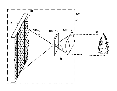
[0012] Figure IA is an illustration of a noise limiting system that
includes an aperture,
according to example embodiments.
[0013] Figure 1B is an illustration of a noise limiting system that
includes an aperture,
according to example embodiments.
[0014] Figure 2 is an illustration of a noise limiting LIDAR device that
includes an aperture,
according to example embodiments.
[0015] Figure 3 is an illustration of a noise limiting system that
includes an aperture, according
to example embodiments.
[0016] Figure 4 is an illustration of a noise limiting system that
includes an aperture, according
to example embodiments.
[0017] Figure 5 is an illustration of a noise limiting system that
includes an aperture, according
to example embodiments.
[0018] Figure 6A is an illustration of an opaque material with various
apertures defined
therein, according to example embodiments.
3c
Date Recue/Date Received 2022-04-27
CA 03039911 2019-04-09
WO 2018/071251
PCT/US2017/055148
10019] Figure 6B is an illustration of a portion of a noise limiting system
that includes
apertures, according to example embodiments.
[0020] Figure 7A is an illustration of an opaque material with a resizable
aperture,
according to example embodiments.
[0021] Figure 7B is an illustration of an opaque material with a resizable
aperture,
according to example embodiments.
10022] Figure 8 is an illustration of an opaque material with an aperture
having an
adjustable location, according to example embodiments.
100231 Figure 9 is a flow diagram of a method, according to example
embodiments.
DETAILED DESCRIPTION
[0024] Example methods and systems are described herein. Any example
embodiment or feature described herein is not necessarily to be construed as
preferred or
advantageous over other embodiments or features. The example embodiments
described
herein are not meant to be limiting. It will be readily understood that
certain aspects of the
disclosed systems and methods can be arranged and combined in a wide variety
of different
configurations, all of which arc contemplated herein.
[0025] Furthermore, the particular arrangements shown in the figures should
not be
viewed as limiting. It should be understood that other embodiments might
include more or
less of each element shown in a given figure. In addition, some of the
illustrated elements
may be combined or omitted. Similarly, an example embodiment may include
elements that
are not illustrated in the figures.
I. Overview
10026] Example embodiments may relate to devices, systems, and methods for
reducing background light imparted onto an array of light detectors. The light
detectors in the
array may be sensing light from a scene (e.g., the light detectors may be a
sensing component
of a LIDAR system).
[0027] One example system can include a lens. The lens may be used to focus
light
from a scene onto a focal plane. However, the lens may also focus background
light not
intended to be observed onto the focal plane (e.g., sunlight within the
scene). In order to
selectively filter the light (i.e., separate background light from light
corresponding to
information within the scene), an opaque material (e.g., selectively etched
metal or a glass
substrate with a mask placed over it) may be placed at the focal plane of the
lens. The opaque
4
CA 03039911 2019-04-09
WO 2018/071251
PCT/US2017/055148
material could be a slab, a sheet, or various other shapes in a variety of
embodiments. Within
the opaque material, an aperture may be defined. The aperture may select a
region of, or the
entirety of, the light of the scene focused by the lens onto the focal plane.
10028] On a backside of the opaque material (i.e., a side of the opaque
material
opposite the lens), the light selected by the aperture may diverge from the
aperture. In the
direction of divergence of the light, the system may include an array of light
detectors (e.g.,
SPADs) disposed some distance from the aperture. This array of light detectors
may detect
the diverging tight (e.g., an intensity of the diverging light). Because the
light is diverging,
the number of light detectors able to fit into a detection area can be larger
than could fit in a
detection area corresponding to the same cone of light at the focal plane of
the lens. This is
due to the fact that the detection area would be more tightly focused, and
thus smaller, at the
focal plane of the lens than at a distance displaced from the aperture. As an
example, an
aperture having a cross-sectional area of 200 gm by 200 gm may occupy an
equivalent area
to hundreds of SPADs (e.g., each SPAD having a cross-sectional area between
200 gin2 and
600 gm). By comparison, if the light diverges away from the aperture to a
distance
corresponding to a circular cross-sectional area having a diameter of 1.33 mm,
the detection
area, at that plane, may occupy an equivalent area to thousands or tens of
thousands of
SPADs.
10029] Further, the distance by which the light detector array is displaced
from the
aperture (i.e., the distance the light detector array is displaced from the
focal plane of the
lens) can vary in various embodiments. The number of light detectors
positioned to detect the
light diverging from the aperture may be increased by increasing the distance
between the
light detector array and the aperture. For example, for scenes that have an
increased amount
of background light, the light detector array could be displaced an increased
distance from the
aperture.
10030] Additionally, in some embodiments, the aperture may be adjustable.
For
example, the cross-sectional area of the aperture could be varied. In some
embodiments, the
cross-sectional area may be defined by an iris that can open or close to
increase or decrease
the opening within the opaque material that defines the aperture.
Alternatively, the aperture
may be a slit within the opaque material that is partially covered by a
retractable shade. The
retractable shade could be retracted or extended to alter the amount of light
transmitted
through the aperture, and thus, change the effective cross-sectional area of
the aperture. Even
further, the opaque material may have multiple apertures defined therein. The
multiple
apertures may have different shapes and/or sizes. Further, the system could
include one or
CA 03039911 2019-04-09
WO 2018/071251
PCT/US2017/055148
more mirrors (e.g., microelectromechanical systems, MEMs, mirrors) that
reflect light from
the lens toward the opaque material. The one or more mirrors could change
angle with
respect to the lens or could change orientation such that a different one of
the mirrors was in
the path of the light focused by the lens. This could allow a different one of
the apertures
defined within the opaque material to be selected, thereby changing the
effective aperture
area.
Example Systems
10031] Figure IA is an illustration of a noise limiting system 100 that
includes an
aperture, according to example embodiments. The system 100 may include an
array 110 of
light detectors 112, an aperture 122 defined within an opaque material 120,
and a lens 130.
The system 100 may measure light 102 scattered by an object 140 within a
scene. The light
102 may also come, at least partially, from background sources. The noise
limiting system
100 may be a part of a LIDAR device (e.g., a LIDAR receiver), in various
embodiments. For
example, the LIDAR device may be used for navigation of an autonomous vehicle.
Further,
in some embodiments, the noise limiting system 100, or portions thereof, may
be contained
within an area that is unexposed to exterior light other than at the lens 130
or aperture 122.
This may prevent ambient light from triggering the light detectors 112 and
adversely
affecting any measurements.
10032] The array 110 is an arrangement of the light detectors 112. In
various
embodiments, the array 110 may have different shapes. As illustrated in Figure
I A, the array
110 may have a rectangular or a square shape. In alternate embodiments, the
array 110 may
be circular. The size of the array 110 may correspond to a cross-sectional
area of the light 110
diverging from the aperture 122, based on the distance the array 110 is
positioned from the
aperture 122. In some embodiments, the array 110 may be movable. The array 110
may be
moveable closer to, or further from, the aperture 122. For example, the array
may be on an
electrical stage capable of translating in one, two, or three dimensions.
100331 Further, the array 110 may have one or more outputs to a computing
device.
The computing device (e.g., a microprocessor) may receive electrical signals
from the array
110 which indicate an intensity of the light 102 incident on the light
detectors 112. The
computing device may use the electrical signals to determine information about
the object
140 (e.g., distance of the object 140 from the aperture 122). In embodiments
where there is a
single connection between the array 110 and the computing device, the light
detectors 112
6
CA 03039911 2019-04-09
WO 2018/071251
PCT/US2017/055148
within the array 110 may be interconnected with one another in parallel. As
such, the array
110 may be an SiPM or an MPPC, depending on the particular arrangement and
type of the
light detectors 112 within the array 110.
[0034] The light detectors 112 may be one of a variety of types. For
example, the
light detectors 112 may be SPADs. SPADs may make use of avalanche breakdown
within a
reverse biased p-n junction (i.e., diode) to increase output current for a
given incident
illumination on the photodetector. Further. SPADs may be able to generate
multiple electron-
hole pairs for a single incident photon. In alternate embodiments, the light
detectors 112 may
be APlls. Both APDs and SPADs may be biased above the avalanche breakdown
voltage.
Such a biasing condition may create a positive feedback loop having a loop
gain that is
greater than one. Thus, APDs and SPADs biased above the threshold avalanche
breakdown
voltage may be single photon sensitive. In still other embodiments, the light
detectors 112
may be photoresistors, charge-coupled devices (CCDs), or photovoltaic cells.
[0035] In various embodiments, the array 110 may include more than one type
of
light detector across the array. For example, if multiple wavelengths are
being detected by the
array 110, the array 110 may comprise some SPADs that are sensitive to one
range of
wavelengths and some SPADs that are sensitive to a different range of
wavelengths. In some
embodiments, the light detectors 110 may be sensitive to wavelengths between
400 nm and
1.6 1.tm (visible and infrared wavelengths). Further the light detectors 110
may have various
sizes and shapes within a given embodiment or across various embodiments. In
example
embodiments, the light detectors 112 may be SPADs that have package sizes that
are 1 %,
.1%, or .01% of the area of the array 110.
[0036] The opaque material 120 may block the light 102 from the scene
(e.g.,
background light) that is focused by the lens 130 from being transmitted to
the array 110. As
such, the opaque material 120 may be configured to block certain background
light that could
adversely affect the accuracy of a measurement performed by the array 110 of
light detectors
112. The opaque material 120, and therefore the aperture 122, may be
positioned at or near a
focal plane of the lens 130. The opaque material 120 may block transmission by
absorbing
the light 102. Additionally or alternatively, the opaque material 120 may
block transmission
by reflecting the light 102. In some embodiments, the opaque material 120 may
be etched
metal. In alternate embodiments, the opaque material 120 may be a polymer
substrate, a
biaxially-oriented polyethylene terephthalate (BoPET) sheet (also referred to
as a Mylar0
sheet), or a glass overlaid with an opaque mask. Other opaque materials are
also possible in
various alternate embodiments.
7
[0037] The aperture 122 provides a port within the opaque material 120
through which the
light 102 may be transmitted. The aperture 122 may be defined within the
opaque material 120 in a
variety of ways. For example, if the opaque material 120 is a metal, the metal
may be etched to define
the aperture 122. Alternatively, if the opaque material 120 is a glass
substrate overlaid with a mask,
the mask may include an aperture 122 defined using photolithography. In
various embodiments, the
aperture 122 may be partially or wholly transparent. For example, if the
opaque material 120 is a glass
substrate overlaid with a mask, the aperture 122 may be defined by the portion
of the glass substrate
not covered by the mask, meaning the aperture 122 is not completely hollow,
but rather is made of
glass. Therefore, the aperture 122 may be nearly, but not entirely,
transparent to the wavelengths of the
light 102 scattered by the object 140 (because most glasses are not 100%
transparent).
[0038] The aperture 122 (in conjunction with the opaque material 120) may
perform to
spatially filter the light 102 from the scene at the focal plane. For example,
the light 102 may be focused
onto the focal plane at a surface the opaque material 120, and the aperture
122 may allow only a portion
of the focused light to be transmitted to the array 110. As such the aperture
122 may behave as an
optical pinhole. In example embodiments, the aperture may have a cross-
sectional area of between .02
mm2 and .06 mm2 (e.g., .04 mm2).
[0039] Although the term "aperture" as used above with respect to the
aperture 122 describes
a recess or hole in an opaque material through which light may be transmitted,
it is understood that the
term "aperture" may include a broad array of optical features. For example, as
used throughout the
present disclosure, the term "aperture" may additionally encompass transparent
or translucent
structures defined within an opaque material through which light can be
partially transmitted. Further,
the term "aperture" may describe a structure that otherwise selectively limits
the passage of light (e.g.,
through reflection or refraction), such as a mirror surrounded by an opaque
material. In one example
embodiment, mirrored arrays surrounded by an opaque material may be arranged
to reflect light in a
certain direction, thereby defining a reflective portion. This reflective
portion may be referred to as an
"aperture".
[0040] The lens 130 may focus the light 102 from the scene onto the focal
plane (e.g., where
the aperture 122 is positioned). In this way, the light intensity collected
from the scene, at the lens 130,
may be maintained while reducing the cross-sectional area over which the light
102 is being projected
(i.e., increasing the spatial power density of the light 102). As such, the
lens 130 may be a converging
lens. As illustrated in Figure 1A, the lens 130 may be a biconvex lens. For
example, the lens may be a
spherical lens. In alternate embodiments, the
8
Date Re9ue/Date Received 2020-08-12
CA 03039911 2019-04-09
WO 2018/071251
PCT/US2017/055148
lens may be a consecutive set of lens positioned one after another (e.g., a
biconvex lens that
focuses light in a first direction and an additional biconvex lens that
focuses light in a second
plane that is orthogonal to the first direction). Other types of lenses are
also possible. In
addition, there may be other free space optics (e.g, mirrors) positioned near
the lens 130 to
aid in focusing the light 102 incident on the lens 130 onto the opaque
material 120.
100411 The object 140 may be any object positioned within a scene
surrounding the
noise limiting system 100. If the noise limiting system 100 is a component of
a receiver of a
LIDAR system, the object 140 may be illuminated by a transmitter of the same
LIDAR
system using the light 102. In example embodiments where the LIDAR system is
used for
navigation on an autonomous vehicle, the object 140 may be pedestrians, other
vehicles,
obstacles (e.g., trees), or road signs.
100421 The light 102, as described above, may be produced by a transmitter
within a
LIDAR device. As illustrated, the light 102 may be scattered by the object
140, focused by
the lens 130, transmitted through the aperture 122 in the opaque material 120,
and measured
by the array 110 of light detectors 112. This sequence may occur (e.g., within
a LIDAR
device) to determine something about the object 140. In some embodiments, the
light
measured by the array may instead be light that scattered from multiple
objects or from no
objects (e.g., light transmitted by a transmitter of a LIDAR device is not
reflected back
toward the LIDAR device, so the lens only focuses ambient light, such as
sunlight).
[0043] In addition, the wavelength of the light 102 used to analyze the
object 140
may be tailored based on the types of objects expected to be within a scene
and their expected
distance from the lens 130. For example, if the objects expected to be within
the scene absorb
all incoming light of 500 nm wavelength, a wavelength other than 500 nm may be
selected to
illuminate the object 140 and to be analyzed by the noise limiting system 100.
The
wavelength of the light 102 (e.g., if transmitted by a transmitter of a LIDAR
device) may
correspond to a source that generates the light 102. For example, if the light
is generated by a
diode laser, the light 102 may be of a wavelength range centered on 900 nm. A
multitude of
different sources may be capable of generating the light 102 (e.g., an optical
fiber amplifier,
various types of lasers, a broadband source with a filter, etc.).
100441 Figure IB is an illustration of the noise limiting system 100
illustrated in
Figure 1A. As indicated, the distance between the object 140 and the lens 130
is 'd', the
distance between the lens 130 and the opaque material 120 (with a rectangular
aperture 126
defined therein, as opposed to the round aperture 122 illustrated in Figure
IA) is ' f. and the
distance between the opaque material 120 and the array 110 is 'x'. In the
embodiment
9
CA 03039911 2019-04-09
WO 2018/071251
PCT/US2017/055148
illustrated, the opaque material 120 and aperture 126 may be positioned at the
focal plane of
the lens (Le., 'f' may be equivalent to the focal length of the lens).
Further, there may be a
filter 160 placed between the lens 130 and the opaque material 120. Also
located at a distance
'd' from the object 140 is an emitter 150 (e.g., a laser with a LIDAR
transmitter) that emits a
signal to be measured by the array 110.
100451 The following
is a mathematical illustration comparing the amount of
background light that is detected by the array 110 to the amount of signal
light that is
detected by the array 110. For the sake of illustration, it is assumed that
the object 140 is
fully illuminated by sunlight at normal incidence, where the sunlight
represents a background
light source. Further, it is assumed that all the light that illuminates the
object 140 is scattered
according to Lambert's cosine law. In addition, it is assumed that all of the
light (both
background and signal) that reaches the plane of the array 110 is fully
detected by the array
110.
10046] The power of
the signal, emitted by the emitter 150õ that reaches the aperture
124, and thus the array 110, can be calculated using the following:
Alens
signal = Ptx x F x ird2
where Psigõai represents the radiant flux (e.g., in W) of the optical signal
emitted by the
emitter 150 that reaches the array 110, P represents the power (e.g., in W)
transmitted by the
emitter 150, Is represents the reflectivity of the object 140 (e.g., taking
into account Lambert's
Cosine Law), and Alen, represents the cross-sectional area of the lens 130.
100471 In addition,
the background light that reaches the lens 130 can be calculated as
follows:
Psun X Tfilter
Phackgroumi =
where Pbackground represents the radiance (e.g., in ) of the
background signal caused by
m-=sr
sunlight scattering off the object 140 arriving on the lens 130 that is within
a wavelength
band that will be selectively passed by the filter 160, Psun represents the
irradiance (e.g., in
¨w ) density due to the sun (i.e., the background source), and "'filter
represents the transmission
m2
coefficient of the filter 160 (e.g., a bandpass optical filter). The factor
of! comes in due to
IL
the assumption of Lambertian scattering off of the object 140 from normal
incidence.
CA 03039911 2019-04-09
WO 2018/071251
PCT/US2017/055148
10048] The aperture 124 reduces the amount of background light permitted to
be
transmitted to the array 110. To calculate the power of the background light
that reaches the
array 110, after being transmitted through the aperture 124, the area of the
aperture 124 is
taken into account. The cross-sectional area of the aperture can be calculated
using the
following:
Aaperture =wxh
where Aaperture represents the surface area of the aperture 126 relative to
the object 140, and
w and h represent the width and height of the aperture 124, respectively. In
addition, if the
lens 130 is a circular lens, the cross-sectional area of the lens is:
diens )2
Aims = (-2
where diens represents the diameter of the lens.
100491 To calculate the background power transmitted to the array 110
through the
aperture 124, the following can be used:
A aperture
background 'background x 2 X 'xlens
where Pbackground represents background power incident on the array 110, and
Aaperture
represents the acceptance solid angle in steradians. The above formula shows
that Phõckgrõd
is the amount of radiance in the background signal after being reduced by the
lens 130 and
then the aperture 124.
[00501 Substituting the above determined values in for Pbackground,
Aaperture, and
Alens the following can be derived:
(PsunTfilter) (wh) ( (dlens )2 5 Uj
ns
Pbackground = X X it ¨2 = sun' filter wit
71- f 4f 2
100511 Further, the quantity ¨f may be referred to as the "F number" of the
lens
(1/ens
130. Thus, with one more substitution, the following can be deduced for
background power:
PS1111 Tfilterwh
Pbackground =
4F2
100521 Making similar substitutions, the following can be deduced for
signal power
transmitted from the emitter 150 that arrives at the array 110:
(diens )2
2 PtxFdfens
Psignal ¨ Ptx X F)< _________________
ird 2 = 4d2
11
CA 03039911 2019-04-09
WO 2018/071251
PCT/US2017/055148
[0053] By comparing
Psign al with Phackground, a signal to noise ratio (SNR) may be
determined. As demonstrated, an inclusion of the aperture 124, particularly
for apertures
having small w and/or small h, the background power can be significantly
reduced with
respect to the signal power. Besides reducing aperture area, increasing the
transmitted power
by the emitter 150, decreasing the transmission coefficient (i.e., reducing an
amount of
background light that gets transmitted through the filter), and increasing the
reflectivity of the
object 140 may be ways of increasing the SNR.. In the case of a pulsed signal,
the shot noise
of the background, as opposed to the power of the background, may be primarily
relevant
when computing the SNR.
[0054] As described
above, the light transmitted through the aperture 124 may
diverge as it approaches the array 110. Due to the divergence, the detection
area at the array
110 of light detectors may be larger than the cross-sectional area of the
aperture 124 at the
focal plane. An increased detection area (e.g., measured in m2) for a given
light power (e.g,
measured in W) leads to a reduced light intensity (e.g., measured in
incident upon the
IT/
array 110.
[0055] The reduction
in light intensity may be particularly beneficial in embodiments
where the array 110 includes SPADs or other light detectors having high
sensitivities. For
example, SPADs derive their sensitivity from a large reverse-bias voltage that
produces
avalanche breakdown within a semiconductor. This avalanche breakdown can be
triggered by
the absorption of a single photon. Once a SPAD absorbs a single photon and the
avalanche
breakdown begins, the SPAD cannot detect additional photons until the SPAD is
quenched
(e.g., by restoring the reverse-bias voltage). The time until the SPAD is
quenched may be
referred to as the recovery time. If additional photons are arriving at time
intervals
approaching the recovery time (e.g., within a factor of ten of the recovery
time), the SPAD
begins to saturate, and the measurements by the SPAD may no longer directly
correlate to the
power of the light incident on the SPAD. Thus, by reducing the light power
incident on any
individual light detector (e.g., SPAD) within the array 110, the light
detectors within the allay
110 (e.g., SPADs) may remain unsaturated. As such, the light measurements by
each
individual SPAT) may have an increased accuracy.
[0056] Figure 2 is an
illustration of a noise limiting LIDAR device 210 that includes
an aperture, according to example embodiments. The LIDAR device 210 may
include a laser
emitter 212, a computing device 214, an array 110 of light detectors, an
opaque material 120
with the aperture defined therein, and a lens 130, The LIDAR device 210 may
use light 102
CA 03039911 2019-04-09
WO 2018/071251
PCT/US2017/055148
to map an object 140 within a scene. The LIDAR device 210 may be used within
an
autonomous vehicle for navigaiion, in example embodiments.
100571 The laser emitter 212 may emit the light 102 which is scattered by
the object
140 in the scene and ultimately measured by the array 110 of light detectors
(e.g., the light
detectors 102 illustrated in Figure IA). In some embodiments, the laser
emitter 212 may
include an optical fiber amplifier or other amplifying system to increase to
power output of
the laser emitter 212. Further, the laser emitter 212 may be a pulsed laser
(as opposed to a
continuous wave, CW, laser), allowing for increased peak power while
maintaining an
equivalent continuous power output.
100581 The computing device 214 may be configured to control components of
the
LIDAR device 210 and to analyze signals received from components of the LIDAR
device
210 (e.g., the array 110 of light detectors 112). The computing device 214 may
include a
processor (e.g., a microprocessor of a microcontroller) that executes
instructions stored
within a memory to perform various actions. The computing device 214 may use
timing
associated with a signal measured by the array 110 to determine a location
(e.g., the distance
from the LIDAR device 210) of the object 140. For example, in embodiments
where the laser
emitter 212 is a pulsed laser, the computing device 214 can monitor timings of
the output
light pulses and compare those timings with timings of the signal pulses
measured by the
array 110. This comparison may allow the computing device 214 to compute the
distance of
the object 140 based on the speed of light mid the time of travel of the light
pulse. In order to
make an accurate comparison between the timing of the output light pulses and
the timing of
the signal pulses measured by the array 110, the computing device 214 may be
configured to
account for parallax (e.g., because the laser emitter 212 and the lens 130 are
not located at the
same location in space).
100591 In some embodiments, the computing device 214 may be configured to
modulate the laser emitter 212 of the LIDAR device 210_ For example, the
computing device
214 may be configured to change the direction of projection of the laser
emitter 212 (e.g., if
the laser emitter 212 is mounted to or includes a mechanical stage). The
computing device
214 may also be configured to modulate the timing, the power, or the
wavelength of the light
102 emitted by the laser emitter 212. Such modulations may include the
addition or removal
of filters from the path of the light 102, in various embodiments.
100601 Additionally, the computing device 214 may be configured to adjust
the
location of the lens 130, the opaque material 120, and the array 110 relative
to one another.
For example, the lens 130 may be on a movable stage that is controlled by the
computing
13
CA 03039911 2019-04-09
WO 2018/071251
PCT/US2017/055148
device 214 to adjust to location of the lens 130, and thus the location of the
focal plane of the
lens 130. Further, the array 110 may be on a separate stage that allows the
array 110 to be
moved relative to the opaque material 120 and the aperture 122. The array 110
may be moved
by the computing device 214 to alter the detection area on the array 110. As
the array 110 is
moved farther from the opaque material 120, the cross-sectional detection area
on the array
110 may increase because the light 102 diverges as the distance from the
aperture 122 is
increased. Therefore, the computing device 214 may move the array 110 to alter
the number
of light detectors 112 illuminated by the diverging light 102.
10061] In some embodiments, the computing device may also be configured to
control the aperture. For example, the aperture may, in some embodiments, be
selectable
from a number of apertures defined within the opaque material. In such
embodiments, a
MEMS mirror located between the lens and the opaque material may be adjustable
by the
computing device to determine to which of the multiple apertures the light is
directed. In
sonic embodiments, the various apertures may have different shapes and sizes.
In still other
embodiments, the aperture may be defined by an iris (or other type of
diaphragm). The iris
may be expanded or contracted by the computing device, for example, to control
the size of
the aperture.
[0062] Figure 3 is an illustration of a noise limiting system 300 that
includes an
aperture, according to example embodiments. Similar to the system 100
illustrated in Figure
IA, the system 300 may include an array 110 of light detectors 112, an
aperture 122 defined
within an opaque material 120, and a lens 130. In addition, the system 300 may
include an
optical filter 302. The system 300 may measure light 102 scattered by an
object 140 within a
scene. The lens 130, the opaque material 120 defined with the aperture 122,
and the array 110
of light detectors 112 may behave analogously as described with respect to
Figure 1A.
[0063] The optical filter 302 may be configured to divert light of
particular
wavelengths away from the array 110. For example, if the noise limiting system
300 is a
component of a LIDAR device (e.g., a detector of a LIDAR device), the optical
filter 302
may divert any light away from the array 110 that is not of the wavelength
range emitted by a
laser emitter of the LIDAR device. Therefore, the optical filter 302 may, at
least partially,
prevent ambient light or background light from adversely affecting the
measurement by the
array 110.
[0064] In various embodiments, the optical filter 302 may be located in
various
positions relative to the array 110. As illustrated in Figure 3, the optical
filter 302 may be
located in between the lens 130 and the opaque material 120. The optical
filter may
14
CA 03039911 2019-04-09
WO 2018/071251
PCT/US2017/055148
alternatively be located between the lens and the object, between the opaque
material and the
array, or on the array itself (e.g., the array may have a screen covering the
surface of the array
that includes the optical filter or each of the light detectors may
individually be covered by a
separate optical filter).
[0065] The optical filter 302 may be an absorptive filter. Additionally or
alternatively,
the optical filter 302 may be a reflective filter. The optical filter 302 may
selectively transmit
wavelengths within a defined wavelength range (i.e., act as a bandpass optical
filter, such as a
monochromatic optical filter), wavelengths outside a defined wavelength range
(i.e., act as a
band-rejection optical filter), wavelengths below a defined threshold (i.e.,
act as a towpass
optical filter), or wavelengths above a defined threshold (i.e., a highpass
optical filter).
Further, in some embodiments, multiple optical filters may be cascaded to
achieve optimized
filtering characteristics (e.g., a lowpass filter cascaded with a highpass
filter to achieve a
bandpass filter characteristic). The optical filter 302 may be a dichroic
filter or cascaded
dichroic filters, in some embodiments. In alternate embodiments, the optical
filter 302 may be
a diffractive filter. A diffractive filter may split the optical path of
background light and
signal light. This may allow separate background tracking, in some
embodiments.
100661 Further, the optical filter 302 may selectively transmit based on
qualities of
light other than wavelength. For example, the optical filter 302 may
selectively transmit light
based on polarization (e.g., horizontally polarized or vertically polarized).
Alternate types of
optical filters are also possible.
100671 Figure 4 is an illustration of a noise limiting system 400 that
includes an
aperture, according to example embodiments. Similar to the system 100
illustrated in Figure
1A, the system 400 may include an array 110 of light detectors 112, an
aperture 122 defined
within an opaque material 120, and a lens 130. The system 400 may also include
an optical
diffuser 402. The system 400 may measure light 102 scattered by an object 140
within a
scene_ The lens 130, the opaque material 120 defined with the aperture 122,
and the array 110
of light detectors 112 may behave analogously as described with respect to
Figure 1A.
100681 The optical diffuser 402 may evenly distribute the power density of
the light
102 transmitted through the aperture 122 among the light detectors 112 by
diffusing the light
102. The optical diffuser 402 may include a sandblasted glass diffuser, a
ground glass
diffuser, or a holographic diffuser, in various embodiments. Other types of
optical diffusers
are also possible. The optical diffuser 402 is one of a group of possible
components that
enhance an aspect of the divergence of the light 102 once the light 102 is
transmitted through
CA 03039911 2019-04-09
WO 2018/071251
PCT/US2017/055148
the aperture 122. Other divergence enhancing components could include optical
waveguides
or fluids with non-unity indices of refraction, for example.
[0069] In various embodiments, the optical diffuser 402 may be located in
various
positions relative to the array 110. As illustrated in Figure 4, the optical
diffuser 402 may be
located in between the opaque material 120 and the array 110. Alternatively,
the optical
diffuser may be located on the array itself (e.g., the array may have a screen
covering the
surface of the array that includes the optical diffuser or each of the light
detectors may
individually be covered by a separate optical diffuser).
100701 Figure 5 is an illustration of a noise limiting system 500 that
includes an
aperture, according to example embodiments. Similar to the system 100
illustrated in Figure
IA, the system 500 may include an array 110 of light detectors 112, an
aperture 122 defined
within an opaque material 120, and a lens 130. The system 500 may further
include mirrors
502. The lens 130, the opaque material 120 defined with the aperture 122, and
the array 110
of light detectors 112 may behave analogously as described with respect to
Figure 1A.
100711 The min-ors 502 may reflect any of the light 102 that is transmitted
through the
aperture 122 that is diverted away from the array 110 (illustrated in Figure 5
by the finely
dashed lines). This process may be referred to as -photon recycling." The
diversion of the
light may occur due to a reflection of the light from a face of the array 110
(e.g., due to a
partially reflective quality of faces of the light detectors 112 or from
interstitial regions in
between faces of the light detectors 112). In such a case, the mirrors 502 may
redirect light
reflected from the face of the array 110 back toward the array 110. Other
inadvertent causes
of light diversion are also possible.
[0072] As illustrated in Figure 5, the mirrors 502 may be curved mirrors.
In alternate
embodiments there may be more or fewer mirrors. For example, in some
embodiments, there
may be a series of planar mirrors directing the light toward the array. In
another alternate
embodiment, there may instead by a single hollow cylinder or hollow cone,
which
encapsulates the light path between the aperture and the array, that has a
reflective inner
surface to redirect the light toward the array. Alternatively, there could be
four mirrors, as
opposed to two, having the shape of the mirrors 502 illustrated in Figure 5
and positioned
around the light path between the aperture and the array. Further, rather than
mirrors, some
embodiments may include a structure in between the aperture and the array that
totally
internally reflects the hat traveling from the aperture to the array (e.g.,
the structure has an
index of refraction that is large enough compared to an index of refraction of
the surrounding
16
CA 03039911 2019-04-09
WO 2018/071251
PCT/US2017/055148
material to induce total internal reflection). Such a structure may be
referred to as a light-
pipe. Various other arrangements, shapes, and sizes of mirrors are also
possible.
100731 Some embodiments may include multiple features described with
respect to
Figures 3-5. For example, an example embodiment may include an optical filter
between the
lens and the opaque material, an optical diffuser between the opaque material
and the array,
and mirrors between the optical diffuser and the array. Further, similar to
the components
within the noise limiting LIDAR device 210 illustrated in Figure 2, the
additional
components illustrated in Figures 3-5 (e.g., the optical filter 302, the
optical diffuser 402, and
the mirrors 502) may also be on movable stages that arc connectable to and
controllable by a
computing device. Other characteristics of these components (e.g., diffusivity
of the optical
diffuser 402 or angle of the mirrors 502) could also be controlled by a
computing device, in
various embodiments.
[0074] Figure 6A is an illustration of an opaque material 610 with various
apertures
defined therein, according to example embodiments. The apertures may be
circular apertures
612 of varying sizes. Additionally or alternatively, the apertures may be
irregular apertures
614. The various circular apertures 612 and the irregular aperture 614 may be
selectable. For
example, the opaque material 610 may be on a mechanical stage (e.g., a
rotational stage or a
translational stage) that can move with respect to a lens (e.g., the lens 130
illustrated in
Figure 1A) and an array of light detectors (e.g., the array 110 of light
detectors 112 illustrated
in Figure 1A) so as to select one of the apertures.
[0075] The circular apertures 612 may vary in radius, thereby allowing
varying
amounts of light to pass through the respective apertures. In some
embodiments, the larger
radius apertures may allow for increased illumination of the array of light
detectors, which
may lead to an increased sensitivity of a corresponding noised limiting system
(e.g., the noise
limiting system 110 illustrated in Figure 1A). However, when measuring scenes
having an
increased amount of background light, the circular apertures 612 having
smaller radius may
be used to block a greater proportion of the background light. Further, each
of the circular
apertures 612 may have different associated optical filters (e.g., overlaying
the respective
aperture or embedded within the respective aperture). For example, one of the
circular
apertures 612 may selectively transmit light within a visible wavelength
range, and another of
the circular apertures 612 may selectively transmit light within an infrared
wavelength range.
As such, a single opaque material 610, having multiple circular apertures 612
defined therein,
may be capable of selectively transmitting light emitted from various sources
(e.g., various
17
CA 03039911 2019-04-09
WO 2018/071251
PCT/US2017/055148
laser emitters 212, as illustrated in Figure 2). Various circular apertures
612 having various
associated optical filters may have similar or different radii.
100761 Irregular apertures may be specifically designed to account for
optical
aberrations within a system. For example, the keyhole shape of the irregular
aperture 614
illustrated in Figure 6A may assist in accounting for parallax occurring
between an emitter
(e.g., the laser emitter 212 illustrated in Figure 2) and a receiver (e.g.,
the lens 130 and the
array 110 of light detectors illustrated in Figure 2 with the opaque material
610 located
therebetween). The parallax may occur if the emitter and the receiver are not
located at the
same position, for example. Other irregular apertures are also possible, such
as specifically
shaped apertures that correspond with particular objects expected to be within
a particular
scene or irregular apertures that select for specific polarizations of light
(e.g., horizontal
polarizations or vertical polarizations).
[0077] Figure 6B is an illustration of a portion of a noise limiting system
that includes
apertures, according to example embodiments. Similar to the noise limiting
system 100 of
Figure IA, the noise limiting system may include a lens 130. The noise
limiting system may
additionally include an opaque material 650 with apertures 652 defined
therein, and an
adjustable MEMS mirror 660. The system may measure light 102 scattered by an
object 140
within a scene.
[0078] The opaque material 650, similar to the opaque material 120
illustrated in
Fiume 1A, may block the light 102 from the scene (e.g., background light) that
is focused by
the lens 130 from being transmitted to an array (e.g., the array 110
illustrated in Figure 1A).
The opaque material 650, and therefore the apertures 652 may be located with
respect to the
MEMS mirror 660 and the lens 130 such that the surface of the opaque material
650 is
located at or near the focal plane of the lens 130. Similar to the embodiment
of the opaque
material 120 illustrated in Figure 1A, the opaque material 650 may include a
metal layer, a
polymer substrate, a BoPET sheet, or a glass overlaid with an opaque mask_
[0079] The apertures 652, as illustrated, may be circular. In alternate
embodiments,
the apertures may be different shapes or sizes. Additionally or alternatively,
in some
embodiments there may be more or fewer apertures than illustrated in Figure
6B. The
apertures 652 may be aligned with respect to the MEMS mirror 660, such that a
portion of the
light 102 reflected by the MEMS mirror 660 passes through one of the apertures
652 and then
intercepts an array of light detectors (e.g., the array 110 of light detectors
112 illustrated in
Figure 1A).
18
CA 03039911 2019-04-09
WO 2018/071251
PCT/US2017/055148
10080] The MEMS mirror 660 may reflect the light 102 that is focused by the
lens
130. The MEMS mirror 660 may rotate about multiple axes such that the
reflected light 102
is directed toward a specific one, or multiple, of the apertures 652. In some
embodiments, the
rotation of the MEMS mirror 660 may be controlled by a computing device (e.g.,
a
microcontroller). Further, in alternate embodiments, there may be a set of
MEMS mirrors that
sequentially reflect the light to direct the light toward one, or multiple, of
the apertures.
Multiple MEMS mirrors could be located on a single MEMS microchip or across
multiple
MEMS microchips, for example.
I0081j In alternate embodiments, the MEMS mirror (or other type of mirror)
may
replace the opaque material with the multiple apertures. For example, a
reflective surface of
the MEMS mirror (or MEMS mirror array) may be surrounded by an opaque material
and the
reflective surface may act to define an aperture. As such, the MEMS mirror may
select a
portion of the light, which is focused by the lens, to reflect toward the
array. The unselected
portion of the light may be absorbed by the opaque material, for example. In
such example
embodiments, the lens and the array may be disposed on the same side of the
mirror. Further,
in such embodiments where the mirror is a MEMS mirror array, the elements in
the MEMS
mirror array could be selectively switched to dynamically define a shape, a
position, or a size
of the reflective surface that defines the aperture.
100821 Figure 7A is an illustration of an opaque material 710 with a
resizable
aperture, according to example embodiments. The opaque material 710 may have a
slit 712
defined therein. Overlaying the opaque material 710 there may be an opaque
shutter 714. The
aperture may be adjusted in size by moving the opaque shutter 714 relative to
the opaque
material 710, thereby varying the covered portion of the slit 712. In such a
way, the aperture
size could be adjusted without varying the direction of projection of light
(e.g., as is done in
the embodiment illustrated in Figure 6B) within a noise limiting system 100.
100831 The opaque material 710, similar to the opaque material 120
illustrated in
Figure 1A, may block light from the scene from being transmitted to an array
(e.g., the array
110 illustrated in Figure 1A). The opaque material 710 may be located at the
focal plane of a
lens, in some embodiments.
100841 The slit 712, without the opaque shutter 714, is analogous to the
aperture of
other embodiments. For example, if the opaque material 710 is a piece of glass
overlaid by an
opaque mask, the slit 712 is the negative region of the mask (i.e., the region
of the mask
where there mask material has been removed, e.g., by photolithography).
Further, the
dimensions of the slit 712 define the largest aperture size for a
corresponding noise limiting
19
CA 03039911 2019-04-09
WO 2018/071251
PCT/US2017/055148
system. As such, the size of the slit 712 is equivalent to the size of the
aperture when the
opaque shutter 714 has been fully retracted from covering the slit 712. In
alternate
embodiments, the slit could have a different shape. For example, the slit may
be shaped so
that when the opaque shutter is translated linearly over the slit, the size of
the slit increases or
decreases exponentially. Alternatively, the slit may be circularly shaped or
irregularly shaped
(e.g., keyhole shaped, such as the irregular aperture 614 illustrated in
Figure 6A). In still
other embodiments, there could be multiple slits, which could be selected from
and/or
adjusted in size based on the location of the opaque shutter.
[00851 The opaque shutter 714 is a material that may be absorptive and/or
reflective
to a range of wavelengths of light. The range of wavelengths may include
wavelengths of
background light within a scene (e.g., if the opaque shutter 714 is a
component of a noise
limiting system within a LIDAR device). In some embodiments, the opaque
shutter 714 could
include a metal sheet, a BoPET sheet, or a polymer substrate. The opaque
shutter 714 may be
configured to move with respect to the opaque material 710 and the slit 712.
For example, in
some embodiments the opaque shutter 714 may be attached to a mechanical stage
that can
move translationally with respect to the opaque material 710 and the slit 712.
Such movement
may be controlled by a computing device (e.g, a microcontroller). In alternate
embodiments,
the opaque material and the slit may, instead, move with respect to the opaque
shutter (e.g.,
the opaque material and the slit are attached to a mechanical stage, rather
than the opaque
shutter).
[0086] Figure 7B is an illustration of an opaque material 760 with a
resizable
aperture, according to example embodiments. The opaque material 760 may be
embedded
with an iris 762. The iris 762 and the opaque material 760 may be fabricated
out of the same
or different materials. The aperture may be an opening defined by the iris
762. Further, the
iris 762 may expand or contract to adjust the size of the aperture. In such a
way, the aperture
size could be adjusted without varying the direction of projection of light
(e.g., as is done in
the embodiment illustrated in Figure 6B) within a noise limiting system 100.
In some
embodiments, the iris may be a standalone free-space optical component, rather
than being
embedded within an opaque material.
100871 The iris 762 may be defined with multiple opaque fins (e.g., sixteen
opaque
fins as illustrated in Figure 7B) that extend or retract to adjust the size of
the aperture defined
by the iris 762. The iris 762 may be a IVLEMS iris, in some embodiments. The
opaque fins
may be metallic, for example. Further, in some embodiments, the extension or
retraction of
the fins of the iris 762 may be controlled by a computing device (e.g., a
microcontroller). A
CA 03039911 2019-04-09
WO 2018/071251
PCT/US2017/055148
maximum extension of the opaque fins may result in the aperture having a
minimum size.
Conversely, a maximum retraction of the opaque fins may result in the aperture
having a
maximum size.
[0088] In alternate embodiments, the opaque material may include an active
or
passive matrix of liquid crystal light modulators, rather than an iris. In
some embodiments,
the matrix may include a patterned conductive electrode array with two
polarizcrs. Between
the two polarizers may be alignment layers and a liquid crystal layer. Such an
arrangement
may be similar to a liquid crystal display device. The matrix could define the
aperture within
the opaque material. For example, the matrix could be arbitrarily adjusted
(e.g, by a
computing device) to select a size, a position, or a shape of the aperture.
Additionally, in
some embodiments, the optical filter may be integrated within the matrix
(e.g., on top or on
bottom of the matrix, or sandwiched between layers of the matrix).
[0089] Figure 8 is an illustration of an opaque material 810 with an
aperture 812
having an adjustable location, according to example embodiments. For example,
the opaque
material 810 may translate in a two-dimensional plane, relative to a lens and
an array of light
detectors (e.g., the lens 130 and the array 110 of light detectors 112 within
the noise limiting
system 100 illustrated in Figure 1A), to move the aperture 812. The opaque
material 810 may
be driven by a stage or an electric motor, in various embodiments. Further,
such a stage or
electric motor may be controlled by a computing device (e.g., a
microcontroller). Similar to
the opaque material 120 illustrated in Figure IA, the opaque material 810 may
be etched
metal, a BoPET sheet, or a glass overlaid with an opaque mask. Other materials
are also
possible.
[0090] The aperture 812 may be a circular aperture, as illustrated in
Figure 8.
Alternatively, the aperture may have another shape, such as an oval, a
rectangle, or an
irregular shape (e.g., a keyhole shape similar to the shape of the irregular
aperture 614
illustrated in Figure 6A). Further, in some embodiments, the opaque material
may have
multiple apertures defined therein (e.g., similar to the opaque material 610
illustrated in
Figure 6A).
Example Processes
[0091] Figure 9 is a flow chart illustration of a method 900, according to
example
embodiments. The method 900 may be performed by the noise limiting system 100
illustrated
in Figure IA, for example.
21
[0092] At block 902, the method 900 includes focusing, by a lens (e.g.,
the lens 130 illustrated
in Figure 1A) disposed relative to a scene, light from the scene onto a focal
plane. The light from the
scene may be scattered by an object (e.g., the object 140 illustrated in
Figure 1A) within the scene, in
some embodiments.
[0093] At block 904, the method 900 includes transmitting, through an
aperture (e.g., the
aperture 122 illustrated in Figure 1A) defined within an opaque material
(e.g., the opaque material 120
illustrated in Figure 1A) disposed at the focal plane of the lens, the light
from the scene. The aperture
has a cross-sectional area.
[0094] At block 906, the method 900 includes diverging, by the light from
the scene
transmitted through the aperture.
[0095] At block 908, the method 900 includes intercepting, by an array of
light detectors
disposed on a side of the focal plane opposite the lens, the diverged light
from the scene. A cross-
sectional area of the array of light detectors that intercept the diverged
light from the scene is greater
than the cross-sectional area of the aperture.
[0096] At block 910, the method 900 includes detecting, by the array of
light detectors, the
intercepted light.
IV. Conclusion
[0097] The above detailed description describes various features and
functions of the disclosed
systems, devices, and methods with reference to the accompanying figures.
While various aspects and
embodiments have been disclosed herein, other aspects and embodiments will be
apparent. The various
aspects and embodiments disclosed herein are for purposes of illustration only
and are not intended to
be limiting. The invention is defined by the claims.
22
Date Re9ue/Date Received 2020-08-12