Note: Descriptions are shown in the official language in which they were submitted.
CA 03044266 2019-05-17
WO 2018/090145
PCT/CA2017/051379
ACCELEROMETER SENSOR
RELATED APPLICATIONS
This patent application claims the benefit of U.S. Provisional Patent
Application No. 62/425,020 filed November 21, 2016 and entitled
"ACCELEROMETER SENSOR."
TECHNICAL FIELD
An embodiment of the present invention relates generally to a Micro-
Electro-Mechanical System (MEMS) device which measures acceleration forces.
More particularly, a further embodiment relates to a MEMS out-of-plane
configuration accelerometer sensor.
BACKGROUND
An accelerometer is a transducer that is used to measure the physical or
measurable acceleration that is experienced by an object. Depending on the
design, the accelerometer responds to accelerations along one, two, or three
axes. While there are examples of MEMS accelerometers without a proof mass
such as is disclosed in US Patent Number US 6,589,433 B2, in a typical MEMS
accelerometer, as are known in the art, an external acceleration results in a
force
applied to a proof mass structure, hence displacing it with respect to a
frame.
The proof mass displacement can be detected through a variety of transduction
mechanisms such as capacitive, piezoresistive, piezoelectric, tunneling,
optical,
heat transfer, Hall Effect, and thermal mechanisms, for example. Among
different
kinds of MEMS accelerometers, those with capacitive interfaces have typically
attracted more attention in manufacturing high performance accelerometers due
to their typical advantages in one or more performance characteristics such as
higher sensitivity, repeatability of the output, temperature stability, design
flexibility, lower cost, and lower power consumption.
In conventional MEMS accelerometer designs, the direction of the proof
mass movement with respect to the frame may typically be either lateral (i.e.,
in-
1
CA 03044266 2019-05-17
WO 2018/090145
PCT/CA2017/051379
plane accelerometers) or vertical (i.e., out-of-plane accelerometers).
Conventional capacitive in-plane accelerometers typically use sets of
interdigitated comb fingers, with one set attached to the proof-mass and
another
to the frame, to achieve relatively large capacitances per unit area in order
to
improve the device sensitivity. Conventional out-of-plane capacitive
accelerometers normally employ the top or bottom surfaces of the proof-mass as
electrodes and measure their relative displacements to electrodes that are
fixed
to the frame and held across a predefined gap below or above the proof-mass.
For a typical MEMS accelerometer design as known in the art, there are
typically several trade-offs to be made between sensitivity, noise, bandwidth,
and
linearity. To achieve high manufacturing yields and low-cost, several
compromises are typically made at different stages of the MEMS design, or the
design of its electronic interface. Typical MEMS accelerometers known in the
art
may have operating bandwidths that range from 10's to 100's of hertz with
noise
spectral densities in the range of 10's of pg/V Hz to several rrig/V Hz (where
g is a
unit of acceleration, g 7-- 9.81m/s2). In some cases, a closed-loop feedback
control
may be used in a conventionally known design to improve the linearity of the
sensor system which might otherwise be limited due to small operating gaps
between the electrodes that are typically needed for high sensitivity.
In US Patent Application Number US 2005/0194652 Al, an accelerometer
is described comprising three distinct layers of a semiconductor material,
where
an upper and a lower layer serve as fixed electrodes and a central layer
serves
as a seismic mass or proof mass as the moving electrode. The central layer
which comprises the seismic mass is connected to the frame by springs. In such
case, the described accelerometer encompasses the seismic mass suspended
between the upper and lower electrodes by the springs connecting it to the
frame
surrounding it. Each fixed electrode thus forms with the seismic mass a
capacitor
whose capacitance depends on the surface area and characteristics of the
seismic mass, the surface area and characteristics of the corresponding first
and
second electrodes, the distance separating these elements and on the
dielectric
2
CA 03044266 2019-05-17
WO 2018/090145
PCT/CA2017/051379
constant of the matter, generally air, existing between them. However, the
disclosed accelerometer requires separate first and second fixed electrodes,
in
addition to spring mechanisms to suspend the seismic mass from the frame and
regulate travel of the seismic mass between the two electrode components.
In US Patent Number US 8,372,677 62, a tri-axis accelerometer is
described, which comprises a substrate, proof mass, and electrodes. In order
to
form the proof mass a portion of the substrate is separated from an exterior
support structure by a plurality of thin etched cavities. An electrically-
conductive
anchor is coupled to the top of the proof mass. A plurality of electrically-
conductive transverse suspension arms or beams (that form flexural springs)
extend laterally from the anchor beyond the lateral edges of the proof mass to
the exterior support structure where they terminate at a plurality of
electrodes.
However, this prior art design also requires multiple separate electrode
elements
and suspension spring elements to suspend the proof mass from the frame and
regulate travel of the proof mass between the multiple separate electrode
components.
In view of the foregoing, there remains a need for new and improved
MEMS accelerometer devices and associated production processes which
address some of the limitations of existing devices and techniques according
to
the prior art. There also remains a need for improved MEMS accelerometer
devices and associated production processes which may desirably provide one
or more of improved sensitivity, reduced noise, design flexibility, simplified
production and manufacturing, and reduced cost of accelerometer production.
SUMMARY
It is an object of the present invention to provide a capacitive
accelerometer sensor and a method for fabricating the same that address some
of the limitations of the prior art. In one embodiment, the present invention
comprises a structural design and general fabrication processes to develop
highly sensitive, low-noise, and wideband accelerometers. In one such aspect,
the device design may desirably be flexible allowing for simple modifications
to
3
CA 03044266 2019-05-17
WO 2018/090145
PCT/CA2017/051379
device performance through straightforward structural adjustments. In one
embodiment, the accelerometer device structure may be based on bonding two
individually patterned substrates, each containing different segments of the
device, together. In such an embodiment, the accelerometer device may
comprise a capacitive interface with a plurality of electrodes formed on each
of
the two substrates that are separated from each other through precise
microfabrication techniques.
In a particular embodiment, a capacitive accelerometer sensor is provided,
comprising a first substrate and a second substrate wherein:
the first substrate comprises a resilient membrane comprising at least one
first electrode and a proof mass attached to the resilient membrane;
the second substrate comprising at least one second electrode; and
wherein the first substrate and the second substrate are bonded to each
other such that the first electrode of the resilient membrane on the first
substrate
faces the second electrode and is separated from the second electrode on the
second substrate by a capacitive gap; and
wherein the first and second substrates comprise a plurality of openings
and electrical contacts electrically connected to each of the first and second
electrodes, respectively.
In another embodiment, the resilient membrane of the capacitive
accelerometer sensor is fabricated on the first substrate by selective removal
of
material from the first substrate. In a further embodiment, the capacitive gap
may be formed between the first and second electrodes by partial removal of
material from at least one of the first and second substrates. In yet another
embodiment, the capacitive gap may be defined by a spacer layer or a plurality
of
spacers between the first and second substrates. In one aspect, at least one
of
the first electrode and the second electrode may comprise an electrically
conductive material deposited on an electrical insulator or semiconductor
material. In another alternative aspect, the first electrode may comprise an
electrically conductive material deposited above an insulating layer on top of
the
first substrate.
4
CA 03044266 2019-05-17
WO 2018/090145
PCT/CA2017/051379
In another embodiment, the second electrode of the capacitive
accelerometer sensor may comprise an electrically conductive material
deposited
on top of an intermediate layer above the second substrate. In a further
embodiment, at least one of the first substrate and the second substrate may
comprise a plurality of layers of different materials.
In a further embodiment, a method of fabricating a capacitive
accelerometer sensor comprising a first substrate and a second substrate is
provided, the method comprising:
forming a resilient membrane and a proof mass attached to said resilient
membrane from said first substrate by selective material removal from said
first
substrate;
forming at least one first electrode on said resilient membrane;
forming at least one second electrode on said second substrate; and
bonding said first substrate to said second substrate such that said first
electrode of said resilient membrane on said first substrate faces said second
electrode and is separated from said second electrode on said second substrate
by a capacitive gap; and
forming a plurality of openings in at least one of said first and second
substrates to expose at least first and a second electrical contacts which are
electrically connected to each of said first and second electrodes,
respectively.
In one such embodiment, the method of fabricating a capacitive
accelerometer sensor comprises using a suitable microfabrication process to
form the resilient membrane and the attached proof mass.
BRIEF DESCRIPTION OF THE DRAWINGS
Systems and methods according to several embodiments of the present
invention will now be described with reference to the accompanying drawing
figures, in which:
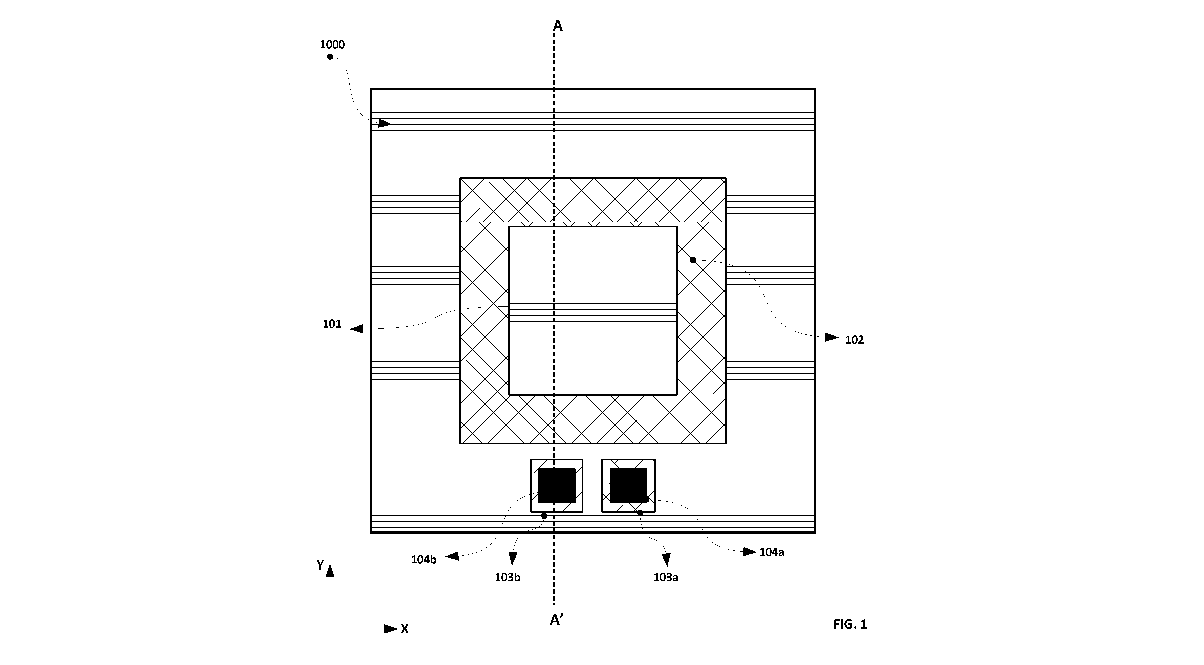
FIG. 1 illustrates a plan view of an exemplary MEMS accelerometer,
comprising a square proof mass and ring accelerometer structure, according to
an embodiment of the invention.
CA 03044266 2019-05-17
WO 2018/090145
PCT/CA2017/051379
FIG. 2 illustrates a cross-sectional view of the accelerometer shown in
FIG. 1 where spacers are used to set the gap between the electrodes, according
to an embodiment of the invention.
FIG. 3 illustrates a plan view of exemplary MEMS accelerometer,
comprising a circular proof-mass and ring membrane accelerometer structure, in
accordance with an embodiment of the invention.
FIG. 4 illustrates a cross-sectional view of an exemplary MEMS
accelerometer, where a multi-layer substrate is used as a first substrate,
according to an embodiment of the present invention.
FIG. 5A illustrates a cross-sectional view of an exemplary MEMS
accelerometer, where the second substrate is electrically isolated from the
conductive layer for the second electrode using an insulating layer, according
to
an embodiment of the invention.
FIG. 5B illustrates a cross-sectional view of an exemplary MEMS
accelerometer, where the second substrate comprises a conducting or
semiconducting material and is used as the second electrode, according to an
embodiment of the invention.
FIG.s 6A, 6B, 6C, 6D and 6E each illustrate a cross-sectional view of an
exemplary electrical contact arrangement for electrical connection of
different
layers of the MEMS accelerometer structure, according to an embodiment of the
invention.
FIG. 7A illustrates a cross-sectional view of an exemplary MEMS
accelerometer, where the gap between the first and second electrodes is
created
by etching a cavity on the second substrate, according to an embodiment of the
invention.
FIG. 7B illustrates a cross-sectional view of an exemplary MEMS
accelerometer, where the gap between the first and second electrodes is
created
by etching a cavity on the first substrate, according to an embodiment of the
invention.
6
CA 03044266 2019-05-17
WO 2018/090145
PCT/CA2017/051379
FIG. 8A illustrates a cross-sectional view of an exemplary MEMS
accelerometer, where dimples are created on the first substrate of the
accelerometer structure, according to an embodiment of the invention.
FIG. 8B illustrates a cross-sectional view of an exemplary MEMS
accelerometer, where dimples are created on the second substrate of the
accelerometer structure, according to an embodiment of the invention.
FIGs. 9A, 9B and 9C each illustrate a plan view of exemplary
embodiments of the electrode on the second substrate of the MEMS
accelerometer, in accordance with an embodiment of the present invention.
FIGs. 10A and 10B illustrate perspective views of a typical accelerometer,
according to an embodiment, that was subjected to experimentation.
FIG. 11 is a graph showing the measured frequency response of the
accelerometer shown in FIGs. 10A and 10B.
FIG. 12 is a graph showing the measured output voltage as a function of
acceleration for a 200Hz sinusoidal input to the accelerometer shown in FIGs.
10A and 10B.
FIG. 13 is a graph showing measured noise as a function of frequency for
the accelerometer shown in FIGs. 10A and 10B.
It will be understood that the above-described drawing figures illustrate
exemplary embodiments of the present invention, and the scope of the present
invention is not limited by the exemplary illustrated embodiments. A more
complete understanding of the present disclosure may be achieved by referring
to the below detailed description and claims, when considered in connection
with
the figures. It should be noted that the figures are not necessarily drawn to
scale.
DETAILED DESCRIPTION OF SEVERAL EMBODIMENTS
In one aspect, an accelerometer sensor may be modeled as a mechanical
mass-spring-damper system. A typical MEMS accelerometer may be
represented as a proof mass, M, that is suspended within a frame using springs
with total stiffness of, K, along the desired axis of sensitivity. Various
forms of
damping may be modeled, such as a damper with damping
7
CA 03044266 2019-05-17
WO 2018/090145 PCT/CA2017/051379
Newton's and Hooke's law imply conservations of energy in the mass-
spring system:
F = Ma = IfAx (1)
where M is the effective mass of proof mass (in kg), dx is its displacement
(in m),
a is input acceleration (in m/s2), and K is the effective spring constant of
the
structure (in N/m). Based on equation (1), the displacement of the proof mass
may be expressed as:
Ma
(2)
The fundamental resonance frequency of accelerometer, coo in rad/s,
which typically limits its useful operational bandwidth, may be given by:
(04 (3)
Substituting equation (3) in (2) leads to,
Lx=- (4)
For capacitive accelerometer devices, this displacement is converted to a
change in capacitance such as by using a variety of electrode configurations.
If
the displacements are measured based on the change in a gap between two
parallel electrodes with effective areas of A separated from each other with
an
initial gap of d, the change in capacitance for lAxl d may be expressed by:
EA EA EA A Co A
¨ LIX = (5)
d d¨Ax d2
where E is the permittivity of the dielectric medium (e.g., air) between the
two
electrodes (in F/m) and Co = is the initial capacitance of the device at
rest.
The accelerometer device response may typically turn nonlinear as Ax becomes
comparable to d due to large input accelerations. The device sensitivity may
be
defined as the change in measured capacitance relative to acceleration applied
to the device and is found from equations (4) and (5):
Sc = (6)
a d tog
8
CA 03044266 2019-05-17
WO 2018/090145
PCT/CA2017/051379
Finally, the spectral density of the Brownian acceleration noise exerted
m/s2
onto the proof mass of the accelerometer, Er7, in may be represented by:
- vliz
an == 4kBT Ea. (7)
MQ
where Q is the quality factor of the device, T is absolute temperature in K,
and
kB is the Boltzmann's constant in J/ K.
As equations (3) to (7) demonstrate, there may typically be tradeoffs
between the operating bandwidth, displacements of the proof mass, sensitivity,
linearity, and noise floor related to the configuration and orientation of a
MEMS
accelerometer design. For example, increasing the proof mass alone leads to a
lower noise, but also reduces the effective operational bandwidth. Increasing
the
spring constant, on the other hand, improves the bandwidth while reducing the
proof mass displacements which ultimately affect the device sensitivity. One
approach to increase the sensitivity of the device is to increase the rate of
change in capacitance per unit displacement through increasing the electrode
area. In one aspect, an out-of-plane accelerometer design may generally offer
relatively large electrode areas. Another method to increase sensitivity may
comprise decreasing the gap between the electrodes. However, this approach
may adversely affect the linearity (i.e., dynamic range) of the accelerometer
device under large input accelerations. To overcome this challenge, most
sensitive accelerometers typically employ a closed-loop control topology to
improve the linear range of operation by applying opposing forces such as
damping forces to the proof mass to reduce its displacements in response to
input accelerations. In one such aspect, the springs attaching the proof mass
to
the frame may typically comprise suspension beams of various shapes. This,
however, may in some cases lead to cross-axis sensitivity of the device to in-
plane accelerations.
In one embodiment according to the present invention, a MEMS
accelerometer structure is described which desirably provides a MEMS
accelerometer structure for the detection of out-of-plane acceleration signals
and
9
CA 03044266 2019-05-17
WO 2018/090145
PCT/CA2017/051379
desirably with low sensitivity to off-axis signals. In one such embodiment,
the
MEMS accelerometer structure may also desirably provide for a sensitive,
wideband and low noise accelerometer sensor.
In a particular embodiment according to the present invention, a MEMS
accelerometer is provided, comprising a proof mass that is attached to a
resilient
membrane made having an integral first electrode, formed from or patterned on
top of a first substrate, and a fixed second electrode on a second substrate
that
is bonded to the first substrate to allow for capacitive detection of proof
mass
displacements by changes in capacitance between the first and second
electrodes. In one aspect, using the entire thickness of the first substrate
for the
proof mass may desirably allow for the design of a low-noise accelerometer
sensor. In another aspect, using a resilient membrane for the spring
suspending
the proof mass may desirably provide for reducing the cross-axis sensitivity
of
the accelerometer device. In yet another aspect, precise bonding processes may
desirably provide for realization of a narrow electrode gap between first and
second electrodes that may desirably improve the sensitivity of the
accelerometer device. In one embodiment, provision of feedback control may be
possible through applying suitable control signals to the second electrode(s)
on
the second substrate.
Referring now to the drawings, in FIG. 1, a plan view of an exemplary
MEMS accelerometer, comprising a square proof mass (101) and square ring
membrane (102) elements of the accelerometer structure is shown, according to
an embodiment of the invention. In one aspect, the MEMS accelerometer may
comprise a body substrate (1000), a proof mass (101) attached to a resilient
membrane (102), a first opening (103a) and membrane electrical contact (104a)
to provide electrical connection to the membrane (102), as well as second
opening (103b) and electrode electrical contact (104b) to provide electrical
connection to the second electrode (104b), which are visible in the plan view
shown as FIG. 1. In one such embodiment, the proof mass (101) and membrane
(102) may be made from the material comprising the first substrate (1000),
such
as by micromachining processes, for example. The resilient membrane (102)
CA 03044266 2019-05-17
WO 2018/090145
PCT/CA2017/051379
may be a solid or continuous structure, or may include one or more openings,
e.g., openings formed by perforation. A cross-sectional view of the MEMS
structure shown in FIG. 1 taken along line A-A' is shown as FIG 2, as detailed
below.
In one such embodiment, the MEMS accelerometer structure may be
fabricated on a suitable first substrate material (1000) such as by selective
removal of mass from the substrate (1000) to form a resilient membrane (102)
and proof mass (101) that is attached to the membrane (102). In addition to
providing the mechanical restoring force as a spring, the resilient membrane
(102), or at least a portion of it, may also be configured to serve as the
first
electrode for the capacitive accelerometer, such as in an exemplary embodiment
where the membrane comprises a conducting or semiconducting material, for
example. In one such embodiment, at least a portion of the resilient membrane
(102) may be configured as a first electrode by any suitable known technique,
such as by applying a film of a conducting and/or semiconducting material
directly to the membrane (102). In a particular embodiment, the membrane (101)
may be comprised of a conductive and/or capacitive material and may thereby
function as a first electrode integrated with the membrane (102). In another
embodiment, the first electrode may be formed by any suitable known technique,
such as by applying a film of a conducting and/or semiconducting material on
an
intermediate layer above the membrane (102).
FIG. 2 illustrates a cross-sectional view of the accelerometer shown in
FIG. 1, where spacers (205) are used to set the gap between the first
electrode
formed by the resilient membrane (201), and the second electrode (206) formed
on a second substrate (2000) which is bonded to the first substrate (1000),
according to an embodiment of the invention. In one such embodiment, a
second electrode (206) may be made on at least a portion of the second
substrate (2000) by any suitable known method, such as by applying a film of a
conductive and/or capacitive material to the second substrate (2000), for
example. In one aspect, the two substrates (1000) and (2000) may then be
bonded to each other such that a gap (203) separates the two electrodes from
11
CA 03044266 2019-05-17
WO 2018/090145
PCT/CA2017/051379
each other and the first and second electrodes remain electrically isolated.
In
another aspect, one or more openings (204) may be provided to expose the first
electrode on membrane (201) and the second electrode (206) on second
substrate (2000) such that the first and second electrodes can be connected to
a
suitable electronic interface (not shown) to provide for measurement of
changes
in capacitance of the accelerometer as the proof mass (202) is displaced with
respect to the second substrate (2000) due to input accelerations. In one
embodiment, one or more openings (204) to expose the first and second
electrodes may be created before or after the bonding of the first and second
substrates (1000) and (2000). In a particular exemplary embodiment shown in
FIG. 2, the gap between the first and second electrodes is set by the
thickness of
one or more spacers (205) situated between the first substrate (1000) and
second substrate (2000) as they are bonded together. In one aspect, the
spacers
(205) may be deposited or placed selectively on one or both of first (1000)
and
second (2000) substrate wafers. In an alternative manufacturing process
according to one embodiment, the spacers (205) may be created by selective
removal of material from one or more thin film(s) that is (are) deposited on
one or
both of first (1000) and second (2000) substrates. In a further variation, a
passage or channel such as a microchannel may be included (a microchannel
through second substrate (2000), for example) that fluidly connects the gap
(203)
with the exterior environment. Such a passage may allow for air to leave or
enter
the gap (203) in response to changes in shape by resilient membrane (201).
In other alternative configurations, various proof mass and membrane
geometries may be substituted in the MEMS accelerometer sensor according to
embodiments of the present invention. FIG. 1 illustrates an exemplary
embodiment showing a top view of a particular accelerometer comprising a
substantially square proof mass (101) and membrane (102) shape, with contact
openings (103a) and (103b) arranged along a side of the accelerometer chip.
In an alternative embodiment, FIG. 3 illustrates a plan view of an
exemplary MEMS accelerometer, comprising a substantially circular proof mass
(301) and resilient ring shaped membrane (303) formed in a first substrate
(1000)
12
CA 03044266 2019-05-17
WO 2018/090145
PCT/CA2017/051379
to form the accelerometer structure, in accordance with another embodiment of
the invention. In one aspect, the accelerometer embodiment shown in FIG. 3
also comprises contact openings (302a) to (302d) arranged around the ring
shaped membrane (303), shown in this embodiment substantially situated at the
corners of the accelerometer chip.
In one embodiment, the first substrate (1000) of the accelerometer
structure can be made from any suitable substrate material or combination of
suitable materials, and the proof mass (101) and resilient membrane (102)
features may be formed in the first substrate (1000) using any suitable
technique
or combination of techniques, such as micro-milling, etching, ablative and/or
other micromachining techniques, for example. In a particular embodiment in
which the first substrate (1000) is made of silicon, a range of suitable known
patterning/etching/ablating techniques adapted for use on silicon based
substrates can be employed to pattern the proof mass (101) and resilient
membrane (102) features of the accelerometer structure based on silicon
microfabrication processes.
In one aspect, the proof mass (101) structure and openings to contacts
with the first electrode and second electrodes can be created through
selective
removal of the substrate material such as by using one or more suitable known
etching techniques. For example, wet etching of crystalline silicon may be
conducted to achieve proof mass and opening structures with predefined
sidewall angles. In another aspect, gas-phase dry etching techniques may be
employed to achieve nearly vertical sidewalls. In a further aspect, the
thickness
of the resilient membrane (102) can be controlled based on the substrate and
employed etching technique. In the simplest such case, the etch depth from the
surface of the first wafer can be controlled through timing the etching
process.
However, timed etching often suffers from non-uniformity across the wafer or
problems limiting repeatability between wafers for batch-fabricated devices.
In an
alternative aspect, another option comprising selecting the desired membrane
thickness through electrochemical and/or dopant-based etch stops. In one such
13
CA 03044266 2019-05-17
WO 2018/090145
PCT/CA2017/051379
aspect, such etch stop techniques may only be applicable to embodiments
utilizing wet etching processes.
In a further embodiment, multi-layer substrates may be used to desirably
simplify the manufacturing process. FIG. 4 illustrates a cross-sectional view
of an
exemplary MEMS accelerometer, where a multi-layer substrate is used as a first
substrate (1000), according to an embodiment of the present invention. In one
such embodiment, the thickness of different substrate layers may be selected
to
define the desired height of the proof mass (401) and desired thickness of the
resilient membrane (402) features on the finished first substrate (1000)
wafer. In
another aspect, suitable selective material removal processes may be employed
to form the proof mass (401) and resilient membrane (402) features, based on
the physical and chemical properties of these substrate material layers.
Accordingly, suitable selective material removal processes may be applied to
particular embodiments utilizing both wet and dry etching processes, for
example. In one aspect, an example of a potentially suitable such multi-layer
substrate is a silicon-on-insulator (S01) wafer. In one such embodiment, an
SOI
wafer may comprise a top silicon layer (i.e., a top device layer), situated on
top of
a typically relatively thin silicon dioxide middle layer (i.e., a middle
buried oxide
layer), which is situated above another bottom silicon layer (i.e., a bottom
handle
layer). In one aspect, in an exemplary MEMS fabrication process, the thickness
of the top device layer may range from a few tens of nm to a few hundreds of
pm,
while the thickness of the middle buried oxide layer may range between a few
tens of nm to a few pm thick, for example. In one aspect, the thickness of the
bottom handle layer may typically be in the range of few hundreds of pm, for
example. In a particular embodiment, the thicknesses of all these layers of
the
multi-layer first substrate (1000) may desirably be simply and precisely
controlled
during the SOI wafer manufacturing process, such as by using suitable known
wafer manufacturing techniques.
As shown in FIG. 4, with a multi-layer first substrate (1000), the proof
mass (401) can be formed from one layer (such as an exemplary silicon handle
layer) and the membrane (402) may be formed from another layer (such as an
14
CA 03044266 2019-05-17
WO 2018/090145
PCT/CA2017/051379
exemplary silicon device layer). For instance, in one particular embodiment,
the
bottom handle wafer of an SOI wafer can be patterned to form the proof mass
(401) and one or more openings (403) to expose contacts. The resilient
membrane (402), on the other hand, can in one such embodiment be formed
from a device layer of an exemplary SOI wafer. In a particular such
embodiment,
the insulating layer (404) of an exemplary SOI wafer may serve as an etch-stop
layer and may optionally be removed, such as from the exposed areas of the
membrane, later if needed or desired.
In one embodiment, the second substrate (2000) layer may be formed
from a suitable electrically insulating material, such as an insulating glass,
for
example, in which case the second electrode may be directly deposited and
patterned on the second substrate layer (2000), such as is shown in the
exemplary embodiment illustrated in FIG 4.
FIG. 5A illustrates a cross-sectional view of an exemplary MEMS
accelerometer according to another embodiment of the present invention, where
the second substrate (2000) is electrically isolated from the conductive layer
for
the second electrode using an insulating layer (501). In one such alternative
aspect, if the second substrate (2000) is made from a conducting or
semiconducting material (e.g., silicon), an electrical insulator layer (501)
may be
deposited on its surface prior to deposition and patterning of the second
electrode as illustrated in the exemplary structure shown in FIG. 5A. In one
such
embodiment, deposition of an intermediate insulating layer (501) may also be
desirable due to fabrication requirements such as the need for an adhesion
layer
or a diffusion barrier, for example.
FIG. 5B illustrates a cross-sectional view of an exemplary MEMS
accelerometer according to another embodiment of the present invention, where
the second substrate (2000) is electrically conducting or semiconducting and
is
used as the second electrode. In one such embodiment, the membrane (503) on
the first substrate functions as the first electrode while the second
substrate
(2000) functions as the second substrate. The first and second electrodes are
separated from each other, such as by using insulating spacers or an
insulating
CA 03044266 2019-05-17
WO 2018/090145
PCT/CA2017/051379
spacer layer (504) that is suitably patterned, also forming the desired
capacitive
gap (502).
In one aspect, electrical connections are typically needed to provide for
connection to the two electrode layers of the first and second substrates
(1000)
and (2000) in order to be able to measure capacitance variations due to
movement of the proof mass.
FIG.s 6A, 6B, 6C, 6D, and 6E each illustrate a cross-sectional view of an
exemplary electrical contact arrangement for electrically connection of
different
substrate layers of the MEMS accelerometer structure, according to an
embodiment of the invention. In one aspect, FIG. 6A illustrates a first
exemplary
electrical contact (601a) is applied to and in conductive contact with the
conducting layer on the surface of the second substrate (2000). In another
aspect, FIG. 6B illustrates a second exemplary electrical contact (601b)
applied
to and in conductive contact with the conducting layer within a cavity etched
on
the surface of the second substrate (2000). In a further aspect, FIG. 6C
illustrates a third exemplary electrical contact (601c) applied to and in
conductive
contact with a conducting layer on the membrane layer (602) of the first
substrate
(1000). In yet a further aspect, FIG. 6D illustrates an exemplary electrical
contact
(601d) applied to and in conductive contact with the handle layer of the first
substrate (1000). In yet a further aspect, FIG. 6E illustrates an exemplary
electrical contact (601e) applied to and in conductive contact with a
conducting
layer on the top of an intermediate layer (603) which is on top of the second
substrate (2000). It is understood that the exemplary first substrate (1000)
and/or
the second substrate (2000) shown in FIG.s 6A, 6B, 6C, 6D, and 6E may be
provided as multi-layer substrates in other aspects of the invention, even
though
a single material substrate is shown for simplicity if the figures. In some
embodiments, it may be desired to provide one larger opening to expose
multiple
electrical contacts to different layers of the first substrate (1000) or
second
substrate (2000) components of the accelerometer structure, for example.
FIG. 7A illustrates a cross-sectional view of an exemplary MEMS
accelerometer, where the gap between the first and second electrodes is
created
16
CA 03044266 2019-05-17
WO 2018/090145
PCT/CA2017/051379
by etching a cavity (701) on the second substrate (2000), according to an
embodiment of the invention. In one such embodiment, the gap between the
electrodes can also be created by etching cavities in each or both of the
first
(1000) and second (2000) substrates. In one such aspect, a spacer layer may
desirably not be required, and the first (1000) and second (2000) substrates
may
desirably be directly bonded to each other. In a particular such embodiment,
the
direct bonding of the first (1000) and second (2000) substrates to each other
without a spacer, may desirably provide for an improved bond quality, and also
may desirably provide for increased process simplicity and/or process
repeatability. In one such aspect, the desired gap between the first and
second
electrodes may be adjusted by modifying the depth of the cavity (701) formed
in
or on one or both of the first and/or second substrates. In the particular
embodiment shown in FIG. 7A, the gap between the electrodes is created by
etching a cavity (701) on the surface of the second substrate (2000). In this
case,
the conducting layer to pattern the second electrode on the second substrate
(2000) may be deposited inside the recessed cavity (701). In one such
embodiment, electrical contact to the membrane layer in the first substrate
(1000)
may be provided by extending a conductive layer from within the cavity(ies)
(701)
to the surface of the second substrate (2000), where it may be pressed
against,
and potentially amalgamate with the material from the first substrate (1000),
thereby providing electrical contact with the membrane portion of the first
substrate (1000).
FIG. 7B illustrates a cross-sectional view of an exemplary MEMS
accelerometer, where the gap between the first and second electrodes is
created
by etching a cavity (702) on the first substrate (1000), according to an
alternative
embodiment of the invention. In one such embodiment, a gap between the first
(1000) and second (2000) substrate may be created by etching a cavity (702) on
the resilient membrane surface of the first substrate (1000), such as by
removing
material from the bottom of the membrane layer of the first substrate (1000).
In a
particular aspect, the gap between the first and second substrates may
alternatively be realized by etching cavities on both first and second
substrates, if
17
CA 03044266 2019-05-17
WO 2018/090145
PCT/CA2017/051379
desired. In another embodiment, both substrates (1000) and (2000) may be
etched to create the capacitive gap between the substrates. It is understood
that
while exemplary multi-layer first substrate (1000) wafers are shown in FIG. 7A
and 7B, the same principles apply to a first substrate wafer made from a
single
material or a first substrate wafer made from a single material with later
modifications to some material properties, such as by using doping, for
example.
In another embodiment, in order to reduce the possibility of stiction of the
flexible
membrane to the second electrode during or after fabrication of the devices,
dimples or other suitable raised or indented textured structures may be
created
on at least a portion of the first substrate or second substrate, such as in a
position to prevent contact of parallel substantially planar surfaces of the
flexible
membrane and second electrode, for example.
FIG. 8A illustrates a cross-sectional view of an exemplary MEMS
accelerometer, where dimples (801), or optionally or other suitable raised or
indented textured structures, are created on the first substrate (1000) of the
accelerometer structure, according to an embodiment of the invention.
FIG. 86 illustrates a cross-sectional view of another exemplary MEMS
accelerometer, where dimples (802), or other suitable raised or indented
textured
structures, are created on the second substrate of the accelerometer
structure,
according to an embodiment of the invention.
FIG.s 9A, 9B and 9C each illustrate a plan view of an exemplary
embodiment of a second electrode patterned on the second substrate of a
MEMS accelerometer, in accordance with an embodiment of the present
invention. In one aspect, FIG. 9A shows a first configuration for the second
electrode on the second substrate (2000) where a single electrode is patterned
and used to measure the displacements of the proof mass suspended above it,
by means of measuring the variation in capacitance between the second
electrode and a first electrode situated on the membrane of the first
substrate
(1000). In a particular embodiment, closed-loop control of the accelerometer
sensor may be desired. In one such embodiment, such closed-loop control may
be provided by applying a suitable DC bias voltage between the first and
second
18
CA 03044266 2019-05-17
WO 2018/090145
PCT/CA2017/051379
electrodes so that the proof mass and attached resilient membrane on the first
substrate (1000) is initially biased, deflected or pulled towards the second
electrode on the second substrate (2000). In one such embodiment, during
accelerometer sensor operation, the bias voltage may be modified so that the
combination of the electrostatic force from the bias voltage, the mechanical
restoring force of the resilient membrane, and the force due to input
accelerations substantially balance each other.
In another aspect, it may be desirably simpler from an interface circuit
design perspective to separate the second electrode into at least two segments
where one segment is used for sensing displacements of the first electrode
attached to the proof mass, and another segment is used to apply an electrical
signal for feedback control, calibration, and/or self-test. FIG. 9B
illustrates a
second such configuration for the second electrode on the second substrate
(2000) where the second electrode is patterned as two concentric segments,
including one central segment and a second peripheral segment, for example.
In a further aspect, it may be desirable to provide additional second
electrode segments for the second electrode on the second substrate (2000),
such as to perform further functions. In one such exemplary embodiment, in-
plane accelerations may be measured through partitioning the second electrode
into four segments as shown in FIG. 9C. In such an aspect, FIG. 9C shows a
third configuration for the second electrode on the second substrate (2000)
where four separate second electrode segments are patterned. In such an
embodiment, out-of-plane accelerations can be detected by measurement of the
change in total capacitance between all four second electrode segments on the
second substrate (2000) and the first electrode attached to the proof mass of
the
first substrate (1000). In-place accelerations along x or y axes may cause
tilting
of the proof mass that can be detected by measuring the difference between the
capacitances of each one of the four second electrode segments and the first
electrode attached to the proof mass, for example. In one aspect, additional
contact openings may be provided to expose each of the second electrode
segments for applying suitable electrical connections to each of the second
19
CA 03044266 2019-05-17
WO 2018/090145
PCT/CA2017/051379
electrode elements. It may be noted that the electrode configurations
illustrated
in FIG.s 9A to 9C are exemplary and for illustrative purposes only and that
other
shapes and numbers of electrodes and electrode segments can be employed to
achieve a desired performance or functionality according to alternative
embodiments of the invention.
Although the preceding description discloses details of structure and
functionality of several exemplary embodiments of the present invention, it
should not be considered as limiting the scope of the invention but rather as
providing explanation and illustration of particular aspects of the invention
so as
to enable a person of skill in the art to understand and practice the
disclosed
embodiments.
FIGS. 10A and 10B are perspective views of an illustrative accelerometer
(1100). As shown in FIG. 10A, accelerometer (1100) includes a proof mass
(1101) with a circular face, a typical contact opening (1102) and a resilient
ring
shaped membrane (1103). A typical electrical contact (1104) is shown disposed
in the typical contact opening (1102). Structures such as a second substrate
layer and spacers and capacitive gap are not depicted in FIG. 10A. The package
or another (1105) support structure may offer, among other things, simple
access
to device electrical ports and protection of the components. In FIG. 10B, the
accelerometer (1100) is assembled into a working model constructed according
to various techniques described above.
The working model, fabricated as a low-noise wide-bandwidth
accelerometer, was subjected to experimentation. Although mathematical
modeling can indicate possible performance, it is recognized that
experimentation with working models can reveal performance aspects (desirable
or undesirable) that are not necessarily predicted by modeling.
While in use, the device may be held at a suitable pressure according to
the application requirements and packaging capabilities. The measured
frequency response of the accelerometer is shown in FIG. 11. This measurement
was conducted under vacuum in order to detect the resonance peak for the
fundamental mode of the structure; FIG. 11 shows this peak at about 5.2 kHz.
All
CA 03044266 2019-05-17
WO 2018/090145
PCT/CA2017/051379
other tests were conducted with the accelerometer kept at atmospheric
pressure.
FIG. 12 illustrates measurements on the linearity of the device response to a
200Hz sinusoidal input using a mechanical shaker. During this test the
accelerometer was subjected to input accelerations from 100mg to 10g without
exhibiting nonlinearity. Experimental data indicate a strong linear
correlation
between acceleration and output voltage, over a range of accelerations,
including
a range of accelerations to which human beings might be subject in the course
of
ordinary activities. Further, the observed linearity indicates precise
evaluation of
factors or quantities related to acceleration, such as velocity, displacement
or
direction. The noise of the accelerometer was measured and separated from
ambient noises using spectral coherence noise measurement technique. As
shown in FIG. 13, the measured noise level from 50-5000 Hz was almost
1pg/V Hz at atmospheric pressure, dominated by circuit noise rather than the
MEMS device. Although mathematical modeling indicated potential for various
aspects of performance, the results of experimentation indicate that the
potential
advantages outlined herein can be readily realized. A notable advantage and
variation of the developed system (in comparison to other accelerometers) is
achieving wide working frequency band and low noise performance in a single
device. A device of this kind could be applied in applications in which other
devices may not perform as well, such as phased-array applications.
While the present invention and its various functional components and
operational functions have been described in particular exemplary embodiments,
the invention may also be implemented in hardware, software, firmware,
middleware or a combination thereof and utilized in systems, subsystems,
components or subcomponents thereof, for example, as circuitry that cooperates
with a processor to perform various method steps. In particular embodiments
implemented at least in part in software, elements of the present invention
may
comprise instructions and/or code segments to perform the necessary tasks.
The program or code segments may be stored in a machine readable medium,
such as a processor readable medium or a computer program product, or
transmitted by a computer data signal embodied in a carrier wave, or a signal
21
CA 03044266 2019-05-17
WO 2018/090145
PCT/CA2017/051379
modulated by a carrier, over a transmission medium or communication link. The
machine readable medium or processor readable medium may include any
medium that can store or transfer information in a form readable and
executable
by a machine, for example a processor, computer, etc. Various functional
components may be implemented as one-piece or multi-piece constructions.
Various components that are attached or are bonded to one another may be so
attached or bonded by any of several attachment or bonding instrumentalities,
in
some cases including one-piece construction.
It will be appreciated that the term "or" as used herein refers to a non-
exclusive "or" unless otherwise indicated (e.g., use of "or else" or "or in
the
alternative").
The exemplary embodiments herein described are not intended to be
exhaustive or to limit the scope of the invention to the precise forms
disclosed.
They are chosen and described to explain the principles of the invention and
its
application and practical use to allow others skilled in the art to comprehend
its
teachings.
As will be apparent to those skilled in the art in light of the foregoing
disclosure, many alterations and modifications are possible in the practice of
this
invention without departing from scope thereof. Accordingly, the scope of the
invention is to be construed in accordance with the substance defined by the
claims.
22