Note: Descriptions are shown in the official language in which they were submitted.
CA 03045072 2019-05-27
SP367825W000
1
Description
Title of Invention: ANTENNA APPARATUS AND WIRELESS
APPARATUS
Technical Field
[0001] The present technology relates to an antenna
apparatus and a wireless apparatus to be applied for
building a domestic wireless network, for example.
Background Art
[0002] A system in which a wireless network is built
in a house and apparatuses such as a personal computer
(PC), a smartphone, a television receiver, and an audio
reproduction system can be connected over a wireless
network has been recently implemented. There is a
multi-path problem as a problem in such wireless
transmission. In a multi-path environment, a reflected
wave is present with respect to a direct arriving wave.
Therefore, a phenomenon that a reception level is
greatly lowered occurs in such a manner that the phases
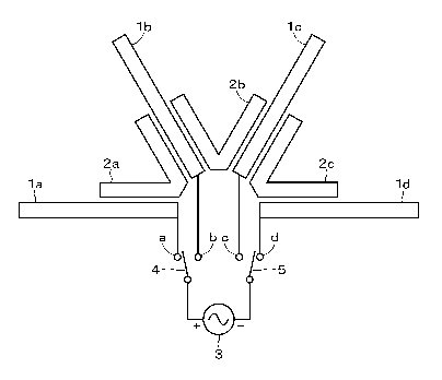
of the direct arriving wave and the reflected wave are
inverted and those waves are received by an antenna, in
a manner that depends on a reception position. In a
case where a reception terminal is small, the terminal
can be set at a best reception position by changing the
Orientation of the terminal. However, in a case of a
large apparatus such as a television receiver and an
CA 03045072 2019-05-27
SP367825W000
2
audio reproduction system, it is difficult to easily
change the orientation and further, it is impossible to
change the orientation also in view of circumstances
associated with a viewing position and a listening
position.
[0003] A diversity antenna , a sector antenna ,
and the like exist as conventional techniques for such
a problem and are generally well known. Those are
techniques of arranging a plurality of antennas apart
from one another to lower the correlation and selecting
an antenna having a highest reception level from among
them. In this technique, the plurality of antennas is
provided as options for each reception position.
Therefore, the multi-path problem is alleviated.
However, in those conventional techniques, firstly, a
plurality of antennas is necessary and secondly,
arrangement of the antennas apart from one another to
provide a lower correlation is necessary, and thus
there is a problem in that a space required for
mounting the antennas becomes larger.
[0004] Patent Literature 1 has described a
configuration in which a switch 3 performs switching
between an antenna apparatus, which is formed by
radially arranging film-like coil elements on a printed
board, and a transceiver. Each of elements Cl to 08 in
the radial form, which are described in Patent
CA 03045072 2019-05-27
SP367825W000
3
Literature 1, is an antenna and varies the directivity
by combining outputs of the plurality of antennas each
having different angles. The switch 3 is adapted to
switch only an output RF signal of the antenna (module
element)
Citation List
Patent Literature
[0005] Patent Literature 1: Japanese Patent
Application Laid-open No. HEI 8-65032
Disclosure of Invention
Technical Problem
[0006] Regarding what is described in Patent
Literature 1, only a power-feeding port is depicted.
However, an antenna necessarily requires a ground area
having the same area as a power-feeding area.
Therefore, there is a problem in that the antenna size
increases. Further, in Patent Literature 1, in order to
feed power to a plurality of ports, it is necessary to
provide distribution and combination devices the number
of which corresponds to the number of power-feeding
units. Therefore, there is a problem in that
distribution loss is generated at the time of sending
and large transmission loss is generated because
combination loss is necessarily generated at the time
of receiving.
[0007] Therefore, it is an object of the present
CA 03045072 2019-05-27
SP367825W000
4
technology to provide an antenna apparatus and a
wireless apparatus in which those problems do not
arise.
Solution to Problem
[0008] The present technology is an antenna
apparatus including:
a plurality of first antenna elements to be
connected to a first power-feeding point; and
a plurality of second antenna elements to be
connected to a second power-feeding point, the
plurality of first antenna elements and the plurality
of second antenna elements being respectively radially
arranged, in which
one of the first antenna elements, which is
selected, is connected to the first power-feeding point
through a first switch apparatus and one of the second
antenna elements, which is selected, is connected to
the second power-feeding point through a second switch
apparatus.
Further, the present technology is a wireless
apparatus that receives a high-frequency signal through
an antenna apparatus and outputs an audio signal and/or
a video signal, the antenna apparatus including
a plurality of first antenna elements to be
connected to a first power-feeding point, and
a plurality of second antenna elements to be
CA 03045072 2019-05-27
SP367825W000
connected to a second power-feeding point, the
plurality of first antenna elements and the plurality
of second antenna elements being respectively radially
arranged, in which
5 one of the first antenna elements, which is
selected, is connected to the first power-feeding point
through a first switch apparatus and one of the second
antenna elements, which is selected, is connected to
the second power-feeding point through a second switch
apparatus.
[0009] In addition, the present technology is an
antenna apparatus including:
two first antenna elements to be connected to a
first power-feeding point; and
two second antenna elements to be connected to a
second power-feeding point, the two first antenna
elements and the two second antenna elements being
respectively radially arranged, in which
switching is performed from a state in which one
of the two first antenna elements, which is selected,
is connected to the first power-feeding point through a
first switch apparatus, to a state in which the other
of the two first antenna elements is connected to one
of the power-feeding points through the first switch
apparatus and
switching is performed from a state in which one
CA 03045072 2019-05-27
SP367825W000
6
of the two second antenna elements, which is selected,
is connected to the second power-feeding point through
a second switch apparatus to a state in which the other
of the two second antenna elements is connected to the
other of the power-feeding points through the second
switch apparatus.
Advantageous Effects of Invention
[0010] In accordance with at least one embodiment,
the present technology requires a small space for
mounting an antenna and further, is capable of reducing
transmission loss. It should be noted that the effect
described here is not necessarily limitative and may be
any effect described in the present technology or an
effect different from these.
Brief Description of Drawings
[0011]
[Fig. 1] Fig. 1 is a block diagram of an embodiment of
a wireless apparatus according to the present
technology.
[Fig. 2] Fig. 2 is a schematic diagram of an
embodiment of an antenna apparatus according to the
present technology.
[Fig. 3] A of Fig. 3, B of Fig. 3, and C of Fig. 3 are
a block diagram, a connection diagram, and a table for
a operation description of an example of a switch
apparatus.
CA 03045072 2019-05-27
SP367825W000
7
[Fig. 4] A of Fig. 4, B of Fig. 4, C of Fig. 4, and D
of Fig. 4 are schematic diagrams to be used for
describing switching of an antenna radiation
directivity of the embodiment of the antenna apparatus.
[Fig. 5] Fig. 5 is a flowchart to be used for an
operation description of an embodiment of a wireless
apparatus according to the present technology.
[Fig. 6] A of Fig. 6 and B of Fig. 6 are schematic
diagrams to be used for describing a modified example
of the antenna apparatus according to the present
technology.
[Fig. 7] Fig. 7 is a schematic diagram to be used for
describing a modified example of the antenna apparatus
according to the present technology.
[Fig. 8] Fig. 8 is a schematic diagram to be used for
describing a modified example of the antenna apparatus
according to the present technology.
Mode(s) for Carrying Out the Invention
[0012] An embodiment described hereinafter is a
favorable specific example of the present technology,
and various technically favorable limitations are added.
However, it should be understood that in the following
descriptions, the range of the present technology is
not limited to those embodiments unless especially it
is indicated that the present technology is limited.
It should be noted that descriptions of the
CA 03045072 2019-05-27
SP367825W000
8
present technology will be made in the order described
below.
<1. Embodiment>
<2. Modified example>
[0013] <1. Embodiment>
Entire Configuration of Wireless Apparatus
Fig. 1 shows a configuration of an embodiment of
the present technology. For example, a wireless local
area network (wireless LAN) is built inside a house 50.
A wireless apparatus 30 as a master performs wireless
communication with a wireless apparatus 20 as a slave.
The wireless apparatus 20 includes a wireless LAN-
compatible audio reproduction apparatus, a speaker
apparatus, a wireless LAN-compatible television
apparatus, and the like. The wireless apparatus 20
includes an antenna apparatus 10 having a variable-
directivity according to the present technology. The
antenna apparatus 10 has radiation directivities 6a, 6b,
and 6c.
[0014] In a case where wireless communication is
performed between the wireless apparatus 20 and the
wireless apparatus 30 within the house 50, a wireless
transmission signal includes signals 40a and 40e as
well as signals 40b, 40c, and 40d. The signals 40b, 40c,
and 40d are direct arriving waves. The signals 40a and
40e are reflected waves reflected on a ceiling and a
CA 03045072 2019-05-27
SP367825W000
9
wall. In such a multi-path environment, the reception
level greatly fluctuates at the antenna apparatus 10
provided in the wireless apparatus 20.
[0015] For example, the wireless transmission
signals 40a and 40b are received by the radiation
directivity 6c. However, in a case where a transmission
distance at which the phases of the wireless
transmission signal 40a and the wireless transmission
signal 40b are inverted and those signals are received,
the reception level is greatly lowered in the antenna
radiation directivity 6c. In a wireless apparatus in
which only one antenna radiation characteristic can be
selected, conventionally, the antenna radiation
directivity 6c can be deviated by moving an
installation location of the wireless apparatus on a
receiver side and the reception condition can be
improved. However, with such a method, it is difficult
to understand to what degree the wireless apparatus
should be moved, the improvement effect is unstable,
and in some cases, there is even a possibility that the
reception condition may be deteriorated.
[0016] At the antenna apparatus 10 of the wireless
apparatus 20 according to the present technology, a
configuration of a power-feeding point switching
antenna is employed. The antenna apparatus 10 is
mounted on a printed circuit board 9. As will be
CA 03045072 2019-05-27
SP367825W000
described later, the antenna apparatus 10 is an antenna
in which the antenna radiation directivity is switched
every time the connection of the antenna to a power-
feeding point 3 is switched through switches 4 and 5.
5 Fig. 1 shows the antenna radiation directivities 6a, 6b,
and 6c.
[0017] A plurality of first antenna elements la and
lb to be connected to a first power-feeding point (+
side, RF signal side) and a plurality of second antenna
10 elements lc and ld to be connected to a second power-
feeding point (- side, ground side)) are radially
arranged. In addition, non-power-feeding elements 2a,
2b, and 2c are provided. The switch 4 connects the +
side of the power-feeding point 3 to one of the antenna
elements la and lb. The switch 5 connects the - side of
the power-feeding point 3 to one of the antenna
elements lc and ld.
[0018] For example, in a case where the antenna
elements la and ld are connected to the power-feeding
point 3 by the switches 4 and 5, a dipole antenna in
which the two antenna elements la and ld face each
other at an angular interval of 180 degrees is
configured. In this case, the antenna radiation
directivity 6b is obtained. In addition, in a case
where the antenna elements la and lc are selected, the
antenna radiation directivity 6b is obtained. In a case
CA 03045072 2019-05-27
SP367825W000
11
where the antenna elements la and lc are selected, the
antenna radiation directivity 6a is obtained. It is the
dipole antenna adapted to select one first element and
one second element.
[0019] A signal received by any of those antenna
radiation directivities is supplied to an RF module 21
as an RF signal processing circuit as an RF signal 23
via a transmission channel formed in the printed
circuit board 9. In the RF module 21, the reception
level in the antenna apparatus 10 is converted into a
numerical value and is supplied to a control apparatus,
for example, a digital signal processor (DSP) 22 as the
status signal 24. Although not shown in the figure, a
signal including information regarding a video signal,
an audio signal, a data signal, and the like is output
from the RF module 21 and a reproduction apparatus
corresponding to each signal is connected to the RF
module 21.
[0020] In the DSP 22, the reception levels of the
plurality of antennas radiation directivities 6a, 6b,
and 6c are compared and a control signal 25 for
selecting the antenna radiation directivity having a
maximum reception level is formed. The control signal
is supplied to the antenna apparatus 10 from the DSP
25 22. In accordance with the control signal 25, the
switches 4 and 5 of the antenna apparatus 10 are
CA 03045072 2019-05-27
SP367825W000
12
controlled and the antenna radiation directivity having
a maximum reception level is selected.
[0021] In controlling the antenna radiation
directivity of the antenna apparatus 10 in this manner,
the wireless apparatus 20 is capable of automatically
selecting an optimal antenna in accordance with a house
environment and an environment fluctuation situation in
the house and realizing best effort communication.
[0022] Antenna Apparatus
The antenna apparatus 10 will be described in
detail with reference to Fig. 2. The antenna apparatus
10 in the embodiment of the present technology includes
the antenna elements la, lb, lc, and ld, the non-power-
feeding elements 2a, 2b, and 2c, the power-feeding
point 3, and the switches 4 and 5. Those components are
mounted on the printed circuit board 9. The antenna
elements la to ld are radially formed at positions on
the printed circuit board 9 to divide a semi-circle at
equiangular intervals of 60 degrees. The non-power-
feeding elements 2a to 2c are formed in regions divided
by the antenna elements adjacent to each other as V-
shaped patterns.
[0023] The switch 4 connects the + side (side on
which the RF signal flows) of the power-feeding point 3
to the power-feeding point of one of the antenna
elements la and lb. The switch 5 connects the - side
CA 03045072 2019-05-27
SP367825W000
13
(ground side) of the power-feeding point 3 to the
power-feeding point of one of the antenna elements lc
and ld. The respective lengths of the antenna elements
la to ld are set to be equal. The lengths of the
antenna elements la to ld are set to receive a signal
having a frequency of a 2.4 GHz band of the wireless
LAN, for example.
[0024] In a case where the power-feeding point 3 is
connected to the two antenna elements through the
switches 4 and 5, a half-wave length dipole antenna is
configured. The total length of the two antenna
elements is set to k/2 (k: one wavelength of a resonant
frequency). In a case where the antenna elements la and
ld are selected, the antenna radiation directivity 6b
is obtained. In a case where the antenna elements la
and lc are selected, the antenna radiation directivity
6a is obtained. In a case where the antenna elements lb
and ld are selected, the antenna radiation directivity
6c is obtained.
[0025] An example of the switch 4 for high frequency,
which has an IC configuration, is shown in A of Fig. 3.
An RF signal terminal is connected to one of terminals
a and b. A power supply voltage VDD and a control
voltage VC are supplied to a decoder 4a provided in the
switch 4. The switch is controlled such that the
decoder 4a selects one of the terminal a or b in
CA 03045072 2019-05-27
SP367825W000
14
accordance with the control voltage VC.
[0026] The switch 4 can be expressed by an
equivalent circuit as shown in B of Fig. 3. The RF
signal terminal is connected to the terminal a (RF1
signal) via two switches Fl and is grounded via a
switch F3 between the two switches Fl. Further, the RF
signal terminal is connected to the terminal b (RF2
signal) via two switches F2 and is grounded via a
switch F4 between the two switches F2.
[0027] An operation of the switch 4 is as shown in
the table of C of Fig. 3. In a case where the control
voltage VC is L (low level), (Fl: ON, F2: OFF, F3: OFF,
F4: ON) is established and the active path becomes (RF-
RF1) (State 1). In a case where the control voltage VC
is H (high level), (Fl: OFF, F2: ON, F3: ON, F4: OFF)
is established and the active path becomes (RF-RF2)
(State 2). A configuration similar to that of the
switch 4 can also be used for the switch 5.
[0028] The operation and action of the above-
mentioned embodiment of the present technology will be
described with reference to Fig. 4. The dipole antenna
is established by the antenna element in which a high-
frequency signal flows and the antenna element which is
a ground. As shown in A of Fig. 4, in a case where the
switch 4 selects the terminal a and the switch 5
selects the terminal c, a dipole antenna having a
CA 03045072 2019-05-27
SP367825W000
facing angle of 120 degrees is constituted by the
antenna element la (shown as oblique lines) and the
antenna element lc (shown as oblique lines). The
antenna radiation directivity 6a along the center line
5 of this dipole antenna is obtained.
[0029] As shown in B of Fig. 4, in a case where the
switch 4 selects the terminal a and the switch 5
selects the terminal d, a dipole antenna having a
facing angle of 180 degrees is constituted by the
10 antenna element la (shown as oblique lines) and the
antenna element ld (shown as oblique lines). The
antenna radiation directivity 6b along the center line
of this dipole antenna is obtained.
[0030] As shown in C of Fig. 4, in a case where the
15 switch 4 selects the terminal b and the switch 5
selects the terminal d, a dipole antenna having a
facing angle of 120 degrees is constituted by the
antenna element lb (shown as oblique lines) and the
antenna element ld (shown as oblique lines). The
antenna radiation directivity 6c along the center line
of this dipole antenna is obtained. In addition, as
shown in D of Fig. 4, the switch 4 may select the
terminal b, the switch 5 may select the terminal c, and
a dipole antenna having a facing angle of 60 degrees
may be constituted by the antenna element lb (shown as
oblique lines) and the antenna element lc (shown as
CA 03045072 2019-05-27
SP367825W000
16
oblique lines). An antenna radiation directivity 6d in
this case has a narrower width while it is further
projected forward.
[0031] In a case where the antenna elements la and
lc are selected (A of Fig. 4), the non-power-feeding
elements 2a and 2b located therebetween are excited and
oscillated by electromagnetic induction at a certain
frequency and radiate a high-frequency signal as the
antenna. An antenna radiation directivity thereof is in
a direction similar to a direction of the antenna
radiation directivity 6a. The resonant frequency
depends on the respective element lengths of the
antenna elements la and lc. By setting the lengths of
the non-power-feeding elements 2a and 2b to lengths
different from the lengths of the antenna elements la
and lc, an antenna compatible for broadband use can be
realized. Lengths when the V-shapes of the non-power-
feeding elements 2a, 2b, and 2c are opened to facing
positions of 180 degrees are the lengths of the non-
power-feeding elements 2a, 2b, and 2c. The lengths of
the non-power-feeding elements 2a, 2b, and 2c are set
to be equal to one another.
[0032] In a case where the antenna elements la and
id are similarly selected (B of Fig. 4), the non-power-
feeding elements 2a, 2b, and 2c located therebetween
are excited and oscillated by electromagnetic induction
CA 03045072 2019-05-27
SP367825W000
17
at a certain frequency and radiate a high-frequency
signal as the antenna. An antenna radiation directivity
thereof is in a direction similar to a direction of the
antenna radiation directivity 6b. In a case where the
antenna elements lb and ld are similarly selected (C of
Fig. 4), the non-power-feeding elements 2b and 2c
located therebetween are excited and oscillated by
electromagnetic induction at a certain frequency and
radiate a high-frequency signal as the antenna. An
antenna radiation directivity thereof is a direction
similar to a direction of the antenna radiation
directivity 6c. By setting the element lengths of the
non-power-feeding elements 2a to 2c to lengths
different from the respective element lengths of the
antenna elements la to ld, a reception band can be made
to be broadband or multi-band.
[0033] In the embodiment of the present technology,
in order to control the antenna radiation directivity,
a control operation performed by the DSP 22 will be
described with reference to the flowchart of Fig. 5.
For example, receiver strength (in Fig. 5, referred to
as receiver signal strength indicator (RSSI)) is used
as an indication representing the intensity of received
radio waves. Additionally, signal to noise ratio (SNR)
may be used as an indication considering the
communication quality as being important. Switching of
CA 03045072 2019-05-27
SP367825W000
18
the reception antenna is performed by controlling the
switches 4 and 5.
[0034] Step ST1: the power supply is activated and
the processing starts.
Step 5T2: the antenna is set to a default antenna
(in Fig. 5, referred to as DEF ANT). For example, the
antenna elements la and id in which the antenna
.
radiation directivity 6b is generated are selected. The
antenna including the antenna elements la and lc in
which the radiation directivity 6a is generated will be
referred to as a left antenna (in Fig. 5, referred to
as LEFT ANT) and the antenna including the antenna
elements lb and id in which the radiation directivity
is generated will be referred to as a right antenna (in
Fig. 5, referred to as RIGHT ANT).
[0035] Step ST3: unconnected
Step ST4: connected
Step ST5: check the receiver strength of each of
the default antenna, the left antenna, and the right
antenna. For example, a mean value of the receiver
strength of the communication packet is checked.
Step ST6: the antenna having a maximum value of
the receiver strength checked in Step 5T5 is set to the
best antenna (in Fig. 5, referred to as BEST ANT) and
best receiver strength (in Fig. 5, referred to as BEST
RSSI) is set.
CA 03045072 2019-05-27
SP367825W000
19
[0036] Step ST7: whether the best receiver strength
is in an alarm status is determined. The alarm status
indicates that the receiver strength is so low that a
favorable reception result cannot be obtained.
Step ST8: in Step ST7, if it is determined that it
is not in the alarm status, the best receiver strength
of the best antenna is updated for each predetermined
time, for example, every second. Then, the processing
returns to Step ST7.
[0037] Step ST9: in Step ST7, if it is determined
that the best receiver strength is in the alarm status,
whether the alarm status continues a plurality of times,
for example, ten times is determined. If it is
determined that the alarm status does not continue ten
times, the processing returns to Step ST7
(determination as to whether the receiver strength is
in the alarm status).
Step ST10: in Step ST9, if it is determined that
the alarm status continues ten times, the receiver
strength of each of the default antenna, the left
antenna, and the right antenna is checked. For example,
the mean value of the receiver strength of the
communication packet is checked.
[0038] Step ST11: out of the receiver strength
checked in Step ST10, the antenna of the receiver
strength of the maximum value is set to the best
CA 03045072 2019-05-27
SP367825W000
antenna and the receiver strength thereof is set to the
best receiver strength.
Step ST12: whether the best receiver strength set
in Step 5T11 is in the alarm status is determined. I it
5 is determined that it is not in the alarm status, the
processing shifts to Step ST8 (updating the best
receiver strength of the best antenna every second).
Step 5T13: in Step ST12, if it is determined that
it is in the alarm status, the best antenna is fixed
10 and the check of the receiver strength is stopped. If
the receiver strength shows out of range, the
processing returns to Step ST2 (setting the antenna to
the default antenna) as shown as *A and performs
antenna setting processing from the beginning.
15 [0039] By the control operation of the DSP 22 as
described above, a best antenna exhibiting a best
directivity can be automatically set. Therefore, it
becomes unnecessary to manually change the orientation
of the wireless apparatus 20 according to the
20 embodiment of the present technology.
[0040] In a case where the multi-path problem is
solved by antenna switching in accordance with the
above-mentioned present technology, it is unnecessary
to provide an installation antenna of a plurality of
antennas as in the conventional one and the antenna
itself is deformed and radiates. Therefore, an antenna
CA 03045072 2019-05-27
SP367825W000
21
capable of switching the radiation directivity in a
saved space can be provided. Further, the V-shaped non-
power-feeding elements compatible for the power-feeding
point switching method are arranged between the antenna
elements, and thus a plurality of frequencies can be
switched at a similar radiation directivity angle.
[0041] <2. Modified Example>
A modified example of a variable-directivity
antenna according to the present technology will be
described. A method of reducing the size of the antenna
will be described with reference to Fig. 6. As shown in
A of Fig. 6, the element lengths can be shortened by
forming the antenna elements 7c and 7d corresponding to
the antenna elements lc and ld in a meander shape. The
same applies to the antenna elements la and lb (not
shown). The element lengths may be shortened by forming
the non-power-feeding elements in a meander shape.
[0042] Further, regarding a non-power-feeding
element Sc corresponding to the non-power-feeding
element 2c, the element length is shortened in such a
manner that chip inductors 11 and 12 are provided at
middle positions of the portions obtained by bending
the element. The same applies to the non-power-feeding
elements 2a and 2b (not shown). The chip inductors may
be provided in the antenna elements and the element
length may be shortened.
CA 03045072 2019-05-27
SP367825W000
22
[0043] As shown in B of Fig. 6, in a case where an
antenna element 13 corresponding to any of the antenna
elements la to ld is formed on the printed circuit
board, it is formed in a spiral shape and electrically
conductive patterns are alternately formed on one
surface of the board and the other surface of the board.
The element length can be shortened by forming the
patterns on the both surfaces. The same applies to the
non-power-feeding element.
[0044] Although the antenna elements la to id are
formed to divide the semi-circle in the antenna
apparatus 10 shown in Fig. 2, antenna elements 14a to
14h may be formed to divide a circle as shown in of Fig.
7. That is, the antenna elements 14a to 14h are
radially formed at positions to divide the circle at
equiangular intervals of 45 degrees. The non-power-
feeding elements 15a to 15h are formed as V-shaped
patterns in regions partitioned by the antenna elements
adjacent to each other. An antenna apparatus shown in
Fig. 7 is capable of switching in a range of 360
degrees. Further, the antenna apparatus shown in Fig. 7
is capable of switching the antenna radiation
directivity with high precision by arranging it at a
narrower angle (45 degrees).
[0045] As shown in of Fig. 8, in a sphere formed
stereoscopically, for example, by rotating a circle C
CA 03045072 2019-05-27
S2367825W000
23
shown as the broken line around a diameter once,
antenna elements 16a, 16b, 16c, and 16d are arranged at
positions to divide the circle C at angular intervals
of 90 degrees and antenna elements 16e, 16f, 16g, and
16h are arranged at positions to divide a circle C at
a position when the circle C is rotated about the
diameter at 90 degrees, at angular intervals of 90
degrees. An antenna apparatus shown in Fig. 8 is
capable of not only switching at an angle on the plane
but also switching of a stereoscopic angle like an
angle of elevation.
[0046] Although the embodiment of the present
technology has been specifically described hereinabove,
the present technology is not limited to the embodiment
and various modifications can be made based on the
technical ideas of the present technology. The
configurations, methods, processes, shapes, materials,
and numerical values, etc. shown in the above-mentioned
embodiments are merely examples and other
configurations, methods, processes, shapes, materials,
and numerical values, etc. may be used depending on
needs.
[0047] It should be noted that the present
technology can also take configurations as follows.
(1) An antenna apparatus, including:
a plurality of first antenna elements to be
CA 03045072 2019-05-27
SP367825W000
24
connected to a first power-feeding point; and
a plurality of second antenna elements to be
connected to a second power-feeding point, the
plurality of first antenna elements and the plurality
of second antenna elements being respectively radially
arranged, in which
one of the first antenna elements, which is
selected, is connected to the first power-feeding point
through a first switch apparatus and one of the second
antenna elements, which is selected, is connected to
the second power-feeding point through a second switch
apparatus.
(2) The antenna apparatus according to (1), in which
the first antenna elements and the second antenna
elements are set to have a substantially equal length.
(3) The antenna apparatus according to (1) or (2), in
which
non-power-feeding elements are respectively
arranged close to the radially arranged first antenna
elements or second antenna elements.
(4) The antenna apparatus according to (3), in which
the first antenna elements, the second antenna
elements, and the non-power-feeding elements are formed
as a pattern of an electric conductor on a printed
circuit board.
(5) The antenna apparatus according to any of (1) to
CA 03045072 2019-05-27
SP367825W000
(4), in which
the first antenna element and the second antenna
element are set to have a substantially equal length
and the non-power-feeding elements are set to have a
5 length different from the length of the first and
second antenna elements.
(6) A wireless apparatus that receives a high-
frequency signal through an antenna apparatus and
outputs an audio signal and/or a video signal, the
10 antenna apparatus including
a plurality of first antenna elements to be
connected to a first power-feeding point, and
a plurality of second antenna elements to be
connected to a second power-feeding point, the
15 plurality of first antenna elements and the plurality
of second antenna elements being respectively radially
arranged, in which
one of the first antenna elements, which is
selected, is connected to the first power-feeding point
20 through a first switch apparatus and one of the second
antenna elements, which is selected, is connected to
the second power-feeding point through a second switch
apparatus.
(7) An antenna apparatus, including:
25 two first antenna elements to be connected to a
first power-feeding point; and
CA 03045072 2019-05-27
SP367825W000
26
two second antenna elements to be connected to a
second power-feeding point, the two first antenna
elements and the two second antenna elements being
respectively radially arranged, in which
switching is performed from a state in which one
of the two first antenna elements, which is selected,
is connected to the first power-feeding point through a
first switch apparatus, to a state in which the other
of the two first antenna elements is connected to one
of the power-feeding points through the first switch
apparatus and
switching is performed from a state in which one
of the two second antenna elements, which is selected,
is connected to the second power-feeding point through
a second switch apparatus to a state in which the other
of the two second antenna elements is connected to the
other of the power-feeding points through the second
switch apparatus.
(8) The antenna apparatus according to (7), in which
the switching of the antenna element through the
first and second switches is performed in such a manner
that directivity of reception is changed.
(9) The antenna apparatus according to (7) or (8), in
which
the first antenna elements and the second antenna
elements are formed as a pattern of an electric
CA 03045072 2019-05-27
S2367825W000
27
conductor on a printed circuit board.
[0048]
la to lh antenna element
2a to 2h non-power-feeding element
3 power-feeding point
4, 5 switch
6a to 6c antenna radiation directivity