Note: Descriptions are shown in the official language in which they were submitted.
CA 03045460 2019-05-29
WO 2018/102652 PCT/US2017/064152
- 1 -
COMPOSITE ELECTRODE
[0001] Related Applications
[0002] The present application claims the benefit of U.S. Provisional
Application No.
62/429,727 entitled "Composite Electrode" and filed December 2, 2016, the
entire contents
of which are incorporated herein by reference.
[0003] Background
[0004] Carbon nanotubes (hereinafter referred to also as "CNTs") are carbon
structures that
exhibit a variety of properties. Many of the properties suggest opportunities
for
improvements in a variety of technology areas. These technology areas include
electronic
device materials, optical materials as well as conducting and other materials.
For example,
CNTs are proving to be useful for energy storage in capacitors.
[0005] However, CNTs are typically expensive to produce and may present
special
challenges during electrode manufacturing. Accordingly, there is a need for an
electrode
material that exhibits the advantageous properties of CNTs while mitigating
the amount of
CNTs included in the material.
[0006] Summary
[0007] The applicants have developed a composite electrode structure that
exhibits
advantageous properties. In some embodiments, the electrode exhibits the
advantageous
properties of CNTs while mitigating the amount of CNTs included in the
material, e.g., to
less than 10% by weight.
[0008] Electrodes of the type described herein may be used in ultracapacitors
to provide high
performance (e.g., high operating, voltage, high operating temperature, high
energy density,
high power density, low equivalent series resistance, etc.).
[0009] In one aspect, an apparatus is disclosed including an active storage
layer including a
network of carbon nanotubes defining void spaces; and a carbonaceous material
located in
the void spaces and bound by the network of carbon nanotubes, wherein the
active layer is
configured to provide energy storage.
CA 03045460 2019-05-29
WO 2018/102652 PCT/US2017/064152
- 2 -
[0010] In some embodiments, the active layer is substantially free from
binding agents. In
some embodiments, the active layer consists of or consists essentially of
carbonaceous
material. In some embodiments, the active layer is bound together by
electrostatic forces
between the carbon nanotubes and the carbonaceous material. In some
embodiments, the
carbonaceous material includes activated carbon.
[0011] In some embodiments, the carbonaceous material includes nanoform carbon
other
than carbon nanotubes.
[0012] In some embodiments, the network of carbon nanotubes makes up less than
50% by
weight of the active layer, less than 10% by weight of the active layer, less
than 5% by
weight of the active layer, or less than 1% by weight of the active layer.
[0013] Some embodiments include an adhesion layer, e.g., a layer consisting of
or consisting
essentially of carbon nanotubes. In some embodiments the adhesion layer is
disposed
between the active laver and an electrically conductive layer.
[0014] In some embodiments, a surface of the conductive layer facing the
adhesion layer
includes a roughened or textured portion. In some embodiments, a surface of
the conductive
layer facing the adhesion layer includes a nanostructured portion. In some
embodiments, the
nanostructured portion includes carbide "nanowhiskers". These nanowhiskers are
thin
elongated structures (e.g., nanorods) that extend generally away from the
surface of the
conductor layer 102. The nanowhiskers may have a radial thickness of less than
100 nm, 50
nm, 25, nm, 10 nm, or less, e.g., in the range of 1 nm to 100 nm or any
subrange thereof. The
nanowhisker may have a longitudinal length that is several to many times its
radial thickness,
e.g., greater than 20 nm, 50 nm, 100 nm, 200 nm, 300, nm, 400, nm, 500 nm, 1
p.m, 5 p.m, 10
p.m, or more, e.g., in the range of 20 nm to 100 p.m or any subrange thereof.
[0015] In some embodiments, the active layer has been annealed to reduce the
presence of
impurities.
[0016] In some embodiments, active layer has been compressed to deform at
least a portion
of the network of carbon nanotubes and carbonaceous material.
[0017] Some embodiments include an electrode including the active layer.
Some
embodiments include an ultracapacitor including the electrode, In some
embodiments, the
CA 03045460 2019-05-29
WO 2018/102652 PCT/US2017/064152
- 3 -
ultracapacitor has an operating voltage greater than 1.0 V, 2.0 V, 2.5 V 3.0
V, 3.1 V, 3.2 V,
3.5 V, 4.0 V or more.
[0018] In some embodiments, the ultracapacitor has a maximum operating
temperature of at
least 250 C at an operating voltage of at least 1.0 V for a lifetime of at
least 1,000 hours. In
some embodiments, the ultracapacitor has a maximum operating temperature of at
least 250
C at an operating voltage of at least 2.0 V for a lifetime of at least 1,000
hours. In some
embodiments, the ultracapacitor has a maximum operating temperature of at
least 250 C at an
operating voltage of at least 3.0 V for a lifetime of at least 1,000 hours. In
some
embodiments, the ultracapacitor has a maximum operating temperature of at
least 250 C at an
operating voltage of at least 4.0 V for a lifetime of at least 1,000 hours. In
some
embodiments, the ultracapacitor has a maximum operating temperature of at
least 300 C at an
operating voltage of at least 1.0 V for a lifetime of at least 1,000 hours. In
some
embodiments, the ultracapacitor has a maximum operating temperature of at
least 300 C at an
operating voltage of at least 2.0 V for a lifetime of at least 1,000 hours. In
some
embodiments, the ultracapacitor has a maximum operating temperature of at
least 300 C at an
operating voltage of at least 3.0 V for a lifetime of at least 1,000 hours. In
some
embodiments, the ultracapacitor has a maximum operating temperature of at
least 300 C at an
operating voltage of at least 4.0 V for a lifetime of at least 1,000 hours.
[0019] In another aspect, a method including: dispersing carbon nanotubes in a
solvent to
form a dispersion; mixing the dispersion with carbonaceous material to form a
slurry;
applying the slurring in a layer; and drying the slurry to substantially
remove the solvent to
form an active layer including a network of carbon nanotubes defining void
spaces and a
carbonaceous material located in the void spaces and bound by the network of
carbon
nanotubes. Some embodiment include forming or applying a layer of carbon
nanotubes to
provide an adhesion layer on a conductive layer.
[0020] In some embodiments, the applying step including applying the slurry
onto the
adhesion layer.
[0021] Various embodiments may include any of the forgoing elements or
features, or any
elements or features described herein either alone or in any suitable
combination.
CA 03045460 2019-05-29
WO 2018/102652 PCT/US2017/064152
- 4 -
[0022] Brief Description of the Drawings
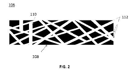
[0023] FIG. 1 is a schematic of an electrode.
[0024] FIG. 2 is an illustration of a detailed view of an active layer of an
electrode.
[0025] FIG. 3 is a schematic of a two-sided electrode.
[0026] FIG. 4 is a flow chart illustrating a method of making an active layer
for an electrode.
[0027] FIG. 5 is a flow chart illustrating a method of making an adhesion
layer for an
electrode.
[0028] FIG. 6 is a schematic diagram of an exemplary mixing apparatus.
[0029] FIG. 7A is a schematic diagram of coating apparatus featuring a slot
die.
[0030] FIG. 7B is a schematic diagram of coating apparatus featuring a doctor
blade.
[0031] FIG. 8A is a schematic of an ultracapacitor.
[0032] FIG. 8B is a schematic of an ultracapacitor without a separator.
[0033] Detailed Description
[0034] Referring to FIG. 1, an exemplary embodiment of an electrode 100 is
disclosed for
use in an energy storage device, such as an ultracapacitor or battery. The
electrode includes
an electrically conductive layer 102 (also referred to herein as a current
collector), an
adhesion layer 104, and an active layer 106. When used in an ultracapacitor of
the type
described herein, the active layer 106 may act as energy storage media, for
example, by
providing a surface interface with an electrolyte (not shown) for formation of
an electric
double layer (sometimes referred to in the art as a Helmholtz layer). In some
embodiments,
the adhesion layer 104 may be omitted, e.g., in cases where the active layer
106 exhibits good
adhesion to the electrically conductive layer 102.
[0035] In some embodiments, the active layer 106 may be thicker than the
adhesion layer
104, e.g., 1.5, 2.0, 5.0, 10, 20, 30, 40, 50, 60, 70, 80, 90, 100, 500, 1,000
or more times the
thickness of the adhesion layer 104. For example, in some embodiments, the
thickness of the
CA 03045460 2019-05-29
WO 2018/102652 PCT/US2017/064152
- 5 -
active layer 106 may be in the range of 1.5 to 1,000 times the thickness of
the adhesion layer
104 (or any subrange thereof, such as 5 to 100 times). For example, in some
embodiments
the active layer 106 may have a thickness in the in the range of 0.5 to 2500
[tm or any
subrange thereof, e.g., 5 [tm to 150 rim. In some embodiments the adhesion
layer 104 may
have a thickness in the range of 0.5 [tm to 50 [tm or any subrange thereof,
e.g., 1 [tm to 5 rim.
[0036] Referring to FIG. 2, in some embodiments, the active layer 106 is
comprised of
carbonaceous material 108 (e.g., activated carbon) bound together by a matrix
110 of CNTs
112 (e.g., a webbing or network formed of CNTs). In some embodiments, e.g.,
where the
length of the CNTs is longer than the thickness of the active layer 106, the
CNTs 112 forming
the matrix 110 may lie primarily parallel to a major surface of the active
layer 106. Not that
although as shown the CNTs 112 form straight segments, in some embodiments,
e.g., where
longer CNTs are used, the some or all of the CNTs may instead have a curved or
serpentine
shape. For example, in cases where the carbonaceous material 108 includes
lumps of
activated carbon, the CNTs 112 may curve and wind between the lumps.
[0037] In some embodiments, the active layer is substantially free of any
other binder
material, such as polymer materials, adhesives, or the like. In other words,
in such
embodiments, the active layer is substantially free from any material other
than carbon. For
example, in some embodiments, the active layer may be at least about 90 wt %,
95 wt %, 96
wt %, 97 wt %, 98 wt %, 99 wt %, 99.5 wt %, 99.9 wt %, 99.99 wt %, 99.999 wt
%, or more
elemental carbon by mass. Despite this, the matrix 110 operated to bind
together the
carbonaceous material 108, e.g., to maintain the structural integrity of the
active layer 106
without flaking, delamination, disintegration, or the like.
[0038] It has been found that use of an active layer substantially free of any
non-carbon
impurities substantially increases the performance of the active layer in the
presence of high
voltage differentials, high temperatures, or both. Not wishing to be bound by
theory, it is
believed that the lack of impurities prevents the occurrence of unwanted
chemical side
reactions which otherwise would be promoted in high temperature or high
voltage conditions.
[0039] As noted above, in some embodiments, the matrix 110 of carbon nanotubes
provides a
structural framework for the active layer 106, with the carbonaceous material
108 filling the
spaces between the CNTs 112 of the matrix 110. In some embodiments,
electrostatic forces
CA 03045460 2019-05-29
WO 2018/102652 PCT/US2017/064152
- 6 -
(e.g., Van Der Waals forces) between the CNTs 112 within the matrix 110 and
between the
matrix 112 and the other carbonaceous material 108 may provide substantially
all of the
binding forces maintaining the structural integrity of the layer.
[0040] In some embodiments, the CNTs 112 may include single wall nanotubes
(SWNT),
double wall nanotubes (DWNT), or multiwall nanotubes (MWNT), or mixtures
thereof.
Although a matrix 110 of individual CNTs 112 is shown, in some embodiments,
the matrix
may include interconnected bundles, clusters or aggregates of CNTs. For
example, in some
embodiments where the CNTs are initially formed as vertically aligned, the
matrix may be
made up at least in part of brush like bundles of aligned CNTs.
[0041] In order to provide some context for the teachings herein, reference is
first made to
U.S. Patent No. 7,897,209, entitled "Apparatus and Method for Producing
Aligned Carbon
Nanotube Aggregate." The foregoing patent (the ¨209 patent") teaches a process
for
producing aligned carbon nanotube aggregate. Accordingly, the teachings of the
'209 patent,
which are but one example of techniques for producing CNTs in the form of an
aligned
carbon nanotube aggregate, may be used to harvest CNTs referred to herein.
Advantageously,
the teachings of the '209 patent may be used to obtain long CNTs having high
purity. In
other embodiments, any other suitable method known in the art for producing
CNTs may be
used.
[0042] In some embodiments the active layer 106 may be formed as follows. A
first
solution (also referred to herein as a slurry) is provided that includes a
solvent and a
dispersion of carbon nanotubes, e.g., vertically aligned carbon nanotubes. A
second solution
(also referred to herein as a slurry) may be provided that includes a solvent
with carbon
disposed therein. This carbon addition includes at least one form of material
that is
substantially composed of carbon. Exemplary forms of the carbon addition
include, for
example, at least one of activated carbon, carbon powder, carbon fibers,
rayon, graphene,
aerogel, nanohorns, carbon nanotubes and the like. While in some embodiments,
the carbon
addition is formed substantially of carbon, it is recognized that in
alternative embodiments
the carbon addition may include at least some impurities, e.g., additives
included by design.
[0043] In some embodiments, forming the first and/or second solution include
introducing
mechanical energy into the mixture of solvent and carbon material, e.g., using
a sonicator
CA 03045460 2019-05-29
WO 2018/102652 PCT/US2017/064152
- 7 -
(sometimes referred to as a sonifier) or other suitable mixing device (e.g., a
high shear
mixer). In some embodiments, the mechanical energy introduced into the mixture
per
kilogram of mixture is at least 0.4 kWh/kg, 0.5 kWh /kg, 0.6 kWh /kg, 0.7 kWh
/kg, 0.8 kWh
/kg, 0.9 kWh /kg, 1.0 kWh /kg, or more. For example, the mechanical energy
introduced into
the mixture per kilogram of mixture may be in the range of 0.4 kWh/kg to 1.0
kWh/kg or any
subrange thereof such as 0.4 kWh/kg to 0.6 kWh/kg.
[0044] In some embodiments, the solvents used may include an anhydrous
solvent. For
example, the solvent may include at least one of ethanol, methanol, isopropyl
alcohol,
dimethyl sulfoxide, dimethylformamide, acetone, acetonitrile, and the like.
[0045] As noted above, the two solutions may be subjected to "sonication"
(physical effects
realized in an ultrasonic field). With regard to the first solution, the
sonication is generally
conducted for a period that is adequate to tease out, fluff or otherwise parse
the carbon
nanotubes. With regard to the second solution, the sonication is generally
conducted for a
period that is adequate to ensure good dispersion or mixing of the carbon
additions within the
solvent. In some embodiments, other techniques for imparting mechanical energy
to the
mixtures may be used in addition or alternative to sonication, e.g., physical
mixing using
stirring or impeller.
[0046] Once one or both of the first solution and the second solution have
been adequately
sonicated, they are then mixed together, to provide a combined solution and
may again be
sonicated. Generally, the combined mixture is sonicated for a period that is
adequate to
ensure good mixing of the carbon nanotubes with the carbon addition. This
second mixing
(followed by suitable application and drying steps as described below) results
in the
formation of the active layer 106 containing the matrix 110 of CNTs 112, with
the carbon
addition providing the other carbonaceous material 108 filling the void spaces
of the matrix
110.
[0047] In some embodiments, mechanical energy may be introduced to the
combined mixture
using a sonicator (sometimes referred to as a sonifier) or other suitable
mixing device (e.g., a
high shear mixer). In some embodiments, the mechanical energy into the mixture
per
kilogram of mixture is at least 0.4 kWh/kg, 0.5 kWh /kg, 0.6 kWh /kg, 0.7 kWh
/kg, 0.8 kWh
/kg, 0.9 kWh /kg, 1.0 kWh /kg, or more. For example, the mechanical energy
introduced into
CA 03045460 2019-05-29
WO 2018/102652 PCT/US2017/064152
- 8 -
the mixture per kilogram of mixture may be in the range of 0.4 kWh/kg to 1.0
kWh/kg or any
subrange thereof such as 0.4 kWh/kg to 0.6 kWh/kg.
[0048] In some embodiments, the combined slurry may be cast wet directly onto
the adhesion
layer 104 or the conductive layer 102, and dried (e.g., by applying heat or
vacuum or both)
until substantially all of the solvent and any other liquids have been
removed, thereby
forming the active layer 106. In some such embodiments it may be desirable to
protect
various parts of the underlying layers (e.g., an underside of a conductive
layer 102 where the
current collector is intended for two sided operation) from the solvent, e.g.,
by masking
certain areas, or providing a drain to direct the solvent.
[0049] In other embodiments, the combined slurry may be dried elsewhere and
then
transferred onto the adhesion layer 104 or the conductive layer 102 to form
the active layer
106, using any suitable technique (e.g., roll-to-roll layer application). In
some embodiments
the wet combined slurry may be placed onto an appropriate surface and dried to
form the
active layer 106. While any material deemed appropriate may be used for the
surface,
exemplary material includes PTFE as subsequent removal from the surface is
facilitated by
the properties thereof. In some embodiments, the active layer 106 is formed in
a press to
provide a layer that exhibits a desired thickness, area and density.
[0050] In some embodiments, the average length of the CNTs 112 forming the
matrix 110
may be at least 0.4.1m, 0.5 pm, 1 pm, 5 pm, 10 pm, 50 pm, 100 pm, 200 pm, 300,
m, 400
pm, 500 m, 600 m, 7000 pm, 800 pm, 900 pm, 1,000 pm or more. For example, in
some
embodiments, the average length of the CNTs 112 forming the matrix 110 may be
in the
range of 1 [tm to 1,000 pm, or any subrange thereof, such as 1 [tm to 600 rim.
In some
embodiments, more than 50%, 60%, 70%, 80%, 90%, 95%, 99% or more of the CNTs
112
may have a length within 10% of the average length of the CNTs 112 making up
the matrix
110.
[0051] In various embodiments, the other carbonaceous material 108 can include
carbon in a
variety forms, including activated carbon, carbon black, graphite, and others.
The
carbonaceous material can include carbon particles, including nanoparticles,
such as
nanotubes, nanorods, graphene in sheet, flake, or curved flake form, and/or
formed into
cones, rods, spheres (buckyballs) and the like.
CA 03045460 2019-05-29
WO 2018/102652 PCT/US2017/064152
- 9 -
[0052] Applicants have found unexpected result that an active layer of the
type herein can
provide exemplary performance (e.g., high conductivity, low resistance, high
voltage
performance, and high energy and power density) even when the mass fraction of
CNTs in
the layer is quite low. For example, in some embodiments, the active layer may
be at least
about 50 wt %, 60 wt %, 70 wt %, 75 wt %, 80 wt %, 85 wt %, 90 wt %, 95 wt %,
96 wt %
97 wt %, 98 wt %, 99 wt %, 99.5 wt %, or more elemental carbon in a form other
than CNT
(e.g., activated carbon). In particular, for certain applications involving
high performance
ultracapacitors, active layers 106 that are in the range of 95 wt % to 99 wt %
activated carbon
(with the balance CNTs 112), have been shown to exhibit excellent performance.
[0053] In some embodiments, the matrix 110 of CNTs 112 form an interconnected
network
of highly electrically conductive paths for current flow (e.g. ion transport)
through the active
layer 106. For example, in some embodiments, highly conductive junctions may
occur at
points where CNTs 112 of the matrix 110 intersect with each other, or where
they are in close
enough proximity to allow for quantum tunneling of charge carriers (e.g.,
ions) from one
CNT to the next. While the CNTs 112 may make up a relatively low mass fraction
of the
active layer (e.g., less than 10 wt %, 5 wt %, 4 wt %, 3 wt %, 2 wt%, 1 wt %
or less, e.g., in
the range of 0.5 wt % to 10 wt % or any subrange thereof such as 1 wt % to 5.0
wt %), the
interconnected network of highly electrically conductive paths formed in the
matrix 110 may
provide long conductive paths to facilitate current flow within and through
the active layer
106 (e.g. conductive paths on the order of the thickness of the active layer
106).
[0054] For example, in some embodiments, the matrix 110 may include one or
more
structures of interconnected CNTs, where the structure has an overall length
in along one or
more dimensions longer than 2, 3, 4, 5, 10, 20, 50, 100, 500, 1,000, 10,000 or
more times the
average length of the component CNTs making up the structure. For example, in
some
embodiments, the matrix 110 may include one or more structures of
interconnected CNTs,
where the structure has an overall in the range of 2 to 10,000 (or any
subrange thereof) times
the average length of the component CNTs making up the structure For example,
in some
embodiments the matrix 110 may include highly conductive pathways having a
length greater
than 100 pm, 500 pm, 1,000 pm, 10,000 pm or more, e.g., in the range of 100 pm
- 10,000
[tm of any subrange thereof.
CA 03045460 2019-05-29
WO 2018/102652 PCT/US2017/064152
- 10 -
[0055] As used herein, the term "highly conductive pathway" is to be
understood as a
pathway formed by interconnected CNTs having an electrical conductivity higher
than the
electrical conductivity of the other carbonaceous material 108 (e.g.,
activated carbon),
surrounding that matrix 110 of CNTs 112.
[0056] Not wishing to be bound by theory, in some embodiments the matrix 110
can
characterized as an electrically interconnected network of CNT exhibiting
connectivity above
a percolation threshold. Percolation threshold is a mathematical concept
related to
percolation theory, which is the formation of long-range connectivity in
random systems.
Below the threshold a so called "giant" connected component of the order of
system size does
not exist; while above it, there exists a giant component of the order of
system size.
[0057] In some embodiments, the percolation threshold can be determined by
increasing the
mass fraction of CNTs 112 in the active layer 106 while measuring the
conductivity of the
layer, holding all other properties of the layer constant. In some such cases,
the threshold can
be identified with the mass fraction at which the conductivity of the layer
sharply increases
and/or the mass fraction above which the conductivity of the layer increases
only slowly with
increases with the addition of more CNTs. Such behavior is indictive of
crossing the
threshold required for the formation of interconnected CNT structures that
provide
conductive pathways with a length on the order of the size of the active layer
106.
[0058] Returning to FIG. 1, in some embodiments, one or both of the active
layer 106 and the
adhesion layer 104 may be treated by applying heat to remove impurities (e.g.,
functional
groups of the CNTs, and impurities such as moisture, oxides, halides, or the
like). For
example, in some embodiments, one or both of the layers can be heated to at
least 100 C, 150
C, 200 C, 250 C, 300 C, 350 C, 400 C, 450 C, 500 C or more for at least 1
minute, 5 minutes,
minutes, 30 minutes, 1 hour, 2 hours, 3 hours, 12 hours, 24 hours, or more.
For example,
in some embodiments the layers may be treated to reduce moisture in the layer
to less that
1,000 ppm, 500 ppm, 100 ppm, 10 ppm, 1 ppm, 0.1 ppm or less.
[0059] Returning to FIG. 1, in some embodiments, the adhesion layer 104 may be
formed of
carbon nanotubes. For example, in some embodiments, the adhesion layer 104 may
be at
least about 50%, 75%, 80%, 90%, 95%, 96% 97%, 98%, 99%, 99.5%, 99.9%, 99.99%,
99.999% by mass CNTs. In some embodiments, the CNTs may be grown directly on
the
CA 03045460 2019-05-29
WO 2018/102652 PCT/US2017/064152
- 11 -
conductive layer 102, e.g., using the chemical vapor deposition techniques
such as those
described in U.S. Patent Pub. No 20150210548 entitled "In-line Manufacture of
Carbon
Nanotubes" and published July 30, 2015. In some embodiments, the CNTs may be
transferred onto the conductive layer 102, e.g., using wet or dry transfer
processes, e.g., of the
type described e.g., in U.S. Patent Pub. No. 20150279578 entitled "High Power
and high
Energy Electrodes Using Carbon Nanotubes" and published October 1, 2015. In
some
embodiments, the adhesion layer 104 adheres to the overlying active layer 106
using
substantially only electrostatic forces (e.g., Van Der Waals attractions)
between the CNTs of
the adhesion layer 104 and the carbon material and CNTs of the active layer
106.
[0060] In some embodiments, the CNTs of the adhesion layer 104 may include
single wall
nanotubes (SWNT), double wall nanotubes (DWNT), or multiwall nanotubes (MWNT),
or
mixtures thereof. In some embodiments the CNTs may be vertically aligned. In
one
particular embodiment, the CNTs of the adhesion layer 104 may be primarily or
entirely
SWNTs and/or DWNTs, while the CNTs of the active layer 106 a primarily or
entirely
MWNTs. For example, in some embodiments, the CNTs of the of the adhesion layer
104
may be at least 75%, at least 90%, at least 95%, at least 99% or more SWNT or
at least 75%,
at least 90%, at least 95%, at least 99% or more DWNT. In some embodiments,
the CNTs of
the of the active layer 106 may be at least 75%, at least 90%, at least 95%,
at least 99% or
more MWNT.
[0061] In some embodiments, the adhesion layer 104 may be formed by applying
pressure to
a layer of carbonaceous material. In some embodiments, this compression
process alters the
structure of the adhesion layer 104 in a way that promotes adhesion to the
active layer 106.
For example, in some embodiments pressure may be applied to layer comprising a
vertically
aligned array of CNT or aggregates of vertically aligned CNT, thereby
deforming or breaking
the CNTs.
[0062] In some embodiments, the adhesion layer may be formed by casting a wet
slurry of
CNTs (with or without additional carbons) mixed with a solvent onto the
conductive layer
102. In various embodiments, similar techniques to those described above for
the formation
of the active layer 106 from a wet slurry may be used.
CA 03045460 2019-05-29
WO 2018/102652 PCT/US2017/064152
- 12 -
[0063] In some embodiments, mechanical energy may be introduced to the wet
slurry using a
sonicator (sometimes referred to as a sonifier) or other suitable mixing
device (e.g., a high
shear mixer). In some embodiments, the mechanical energy into the mixture per
kilogram of
mixture is at least 0.4 kWh/kg, 0.5 kWh /kg, 0.6 kWh /kg, 0.7 kWh /kg, 0.8 kWh
/kg, 0.9
kWh /kg, 1.0 kWh /kg, or more. For example, the mechanical energy introduced
into the
mixture per kilogram of mixture may be in the range of 0.4 kWh/kg to 1.0
kWh/kg or any
subrange thereof such as 0.4 kWh/kg to 0.6 kWh/kg.
[0064] In some embodiments, the solid carbon fraction of the wet slurry may be
less than 10
wt %, 5 wt %, 4 wt %, 3 wt %, 2 wt%, 1 wt ,0.5 wt 5,0.1 wt % or less, e.g., in
the range of
0.1 wt % to 10 wt % or any subrange thereof such as 0.1 wt % to 2 wt %.
[0065] In various embodiments, the conductive layer 102 may be made of a
suitable
electrically conductive material such as a metal foil (e.g., an aluminum
foil). In some
embodiments, the surface of the conductive layer 102 may be roughened,
patterned, or
otherwise texturized, e.g., to promote adhesion to the adhesion layer 104 and
good electrical
conductance from the active layer 106. For example, in some embodiments, the
conductive
layer may be etched (e.g., mechanically or chemically). In some embodiments,
the
conductive layer 102 may have a thickness in the range of 1 [tm to 1,000 [tm
or any subrange
thereof such as 5 [tm to 50 rim.
[0066] In some embodiments, the conductive layer 102 may include a
nanostructured
surface. For example, as described in International Pub. No. WO 2016/057983
entitled
"Nanostructured Electrode for Energy Storage Device" published April 14, 2016,
the
conductive layer may have a top surface that includes nanoscale features such
as whiskers
(e.g., carbide whiskers) that promote adhesion to the adhesion layer 104 and
good electrical
conductance from the active layer 106. An exemplary current collector is the
current
collector available from Toyo Aluminum K.K. under the trade name TOYAL-CARBO .
[0067] In some embodiments, one or both of the active layer 106 and the
adhesion layer 104
may be treated by applying heat and/or vacuum to remove impurities (e.g.,
functional groups
of the CNTs, and impurities such as moisture, oxides, halides, or the like).
[0068] In some embodiments, one or both of the active the active layer 106 and
the adhesion
layer 104 may be compressed, e.g., to break some of the constituent CNTs or
other
CA 03045460 2019-05-29
WO 2018/102652 PCT/US2017/064152
- 13 -
carbonaceous material to increase the surface area of the respective layer. In
some
embodiments, this compression treatment may increase one or more of adhesion
between the
layers, ion transport rate within the layers, and the surface area of the
layers. In various
embodiments, compression can be applied before or after the respective layer
is applied to or
formed on the electrode 100.
[0069] In some embodiments, the adhesion layer 104 may be omitted, such that
the active
layer 106 is disposed directly on the conductive layer 102.
[0070] Referring to FIG. 3, in some embodiments, the electrode 100 may be
double sided,
with an adhesion layer 104 and active layer 106 formed on each of two opposing
major
surfaces of the conductive layer 102. In some embodiments, the adhesion layer
104 may be
omitted on one or both sides of the two-sided electrode 100.
[0071] Referring to FIG. 4, an exemplary embodiment of method 200 of making
the active
layer 106 of electrode 100 is described. In step 201, CNTs are dispersed in a
solvent to form
a dispersion of CNTs. In some embodiments, the dispersion may be formed using
any of the
techniques described in U.S. Patent Pub. No. 20150279578 entitled "High Power
and High
Energy Electrodes Using Carbon Nanotubes" published October 1, 2015 including
stirring,
sonication, or a combination of the two. In various embodiments, any suitable
solvent may
be used, including, for example. ethanol, methanol, isopropyl alcohol,
dimethyl sulfoxide,
dimethylformamide, acetone, acetonitrile, and the like. In general, it is
advantageous to
choose a solvent that will be substantially eliminated in the drying step 204
described below,
e.g., using heat and/or vacuum drying techniques.
[0072] In some embodiments, the mixture of CNTs and solvents may be passed
through a
filter, e.g., an array of micro channels (e.g., having channels with diameters
on the order of
the radial size of the CNTs) to help physically separate the CNTs and promote
dispersion.
[0073] In some embodiments, the CNT dispersion may be formed without the
addition of
surfactants, e.g., to avoid the presence of impurities derived from these
surfactants at the
completion of the method 200.
[0074] In step 202, the CNT dispersion is mixed with carbonaceous material
(e.g., activated
carbon) to form a slurry. In some embodiments, the slurry may be formed using
any of the
CA 03045460 2019-05-29
WO 2018/102652 PCT/US2017/064152
- 14 -
techniques described in U.S. Patent Pub. No. 20150279578, published on October
1, 2015,
including stirring, sonication, or a combination of the two. In some
embodiments, the slurry
may have solid carbon fraction of less than 20 wt %, 15 wt %, 10 wt %, 5 wt %,
2 wt %, 1 wt
%, or less, e.g., in the range of 1 wt % to 20 wt % or any subrange thereof
such as 4% to 6%.
The mass ratio of CNTs to other carbonaceous material in the slurry may be
less than 1:5,
1:10, 1:15, 1:20, 1:50, 1:100, or less, e.g., in the range of 1:10 to 1:20 or
any subrange
thereof.
[0075] In step 203, the slurry is applied to either the adhesion layer 104 or,
if the adhesion
layer 104 is omitted, the conductive layer 102 of the electrode 100. In some
embodiments,
the slurry may be formed into a sheet, and coated onto the electrode. For
example, in some
embodiments, slurry may be applied to through a slot die to control the
thickness of the
applied layer. In other embodiments, the slurry may be applied to the
conductive layer 102,
and then leveled to a desired thickness, e.g., using a doctor blade.
[0076] In some embodiments, the slurry may be compressed (e.g., using a
calendaring
apparatus) before or after being applied to the electrode 100. In some
embodiments, the
slurry may be partially or completely dried (e.g., by applying heat, vacuum or
a combination
thereof) during this step 203.
[0077] In step 204, if the slurry has not dried, or has been only partially
dried during step
203, the slurry applied to the electrode is fully dried, (e.g., by applying
heat, vacuum or a
combination thereof). In some embodiments, substantially all of the solvent
(and any other
non-carbonaceous material such as dispersing agents) is removed from the
active layer 106.
In some embodiments, if impurities remain following the drying step, and
additional step of
heating (e.g. baking or annealing) the layer may be performed. For example, in
some
embodiments, one or both of the active the active layer 106 and the adhesion
layer 104 may
be treated by applying heat to remove impurities (e.g., functional groups of
the CNTs, and
impurities such as moisture, oxides, halides, or the like).
[0078] Referring to FIG. 5, an exemplary embodiment of method 300 of making
the adhesion
layer 104 of electrode 100 is described. In step 301, CNTs are dispersed in a
solvent to form
a dispersion of CNTs. In some embodiments, the dispersion may be formed using
any of the
techniques described in U.S. Patent Pub. No. 20150279578, published on October
1, 2015,
CA 03045460 2019-05-29
WO 2018/102652 PCT/US2017/064152
- 1 5 -
including stirring, sonication, or a combination of the two. In various
embodiments, any
suitable solvent may be used, including, for example an organic solvent such
as isopropyl
alcohol, acetonitrile or propylene carbonate. In general, it is advantageous
to choose a
solvent that will be substantially eliminated in the drying step 304 described
below.
[0079] In some embodiments, the mixture of CNTs and solvents may be passed
through a
filter, e.g., an array of micro channels (e.g., having channels with diameters
on the order of
the radial size of the CNTs) to help physically separate the CNTs and promote
dispersion.
[0080] In some embodiments, the CNT dispersion may be formed without the
addition of
surfactants, e.g., to avoid the presence of impurities derived from these
surfactants at the
completion of the method 300.
[0081] In step 302, the CNT dispersion may optionally be mixed with additional
carbonaceous material (e.g., activated carbon) to form a slurry. In some
embodiments, the
additional carbonaceous material may be omitted, such that the slurry is made
up of CNTs
dispersed in a solvent. In some embodiments, the slurry may have solid
fraction of less than
wt %, 4 wt %, 3 wt %, 2 wt %, 1 wt %, 0.5 wt %, 0.1 wt %, or less, e.g., in
the range of 0.1
to 5 wt % or any subrange thereof.
[0082] In step 303, the slurry is applied to the conductive layer 102 of the
electrode 100. In
some embodiments, the slurry may be coated onto the electrode. For example, in
some
embodiments, slurry may be applied to through a slot die to control the
thickness of the
applied layer. In other embodiments, the slurry may be applied to the
conductive layer 102,
and then leveled to a desired thickness, e.g., using a doctor blade.
[0083] In some embodiments, the slurry may be compressed (e.g., using a
calendaring
apparatus) before or after being applied to the electrode 100. In some
embodiments, the
slurry may be partially or completely dried (e.g., by applying heat, vacuum or
a combination
thereof) during this step 303.
[0084] In step 304, if the slurry has not dried, or has been only partially
dried during step
203, the slurry applied to the electrode is fully dried, (e.g., by applying
heat, vacuum or a
combination thereof). In some embodiments, substantially all of the solvent
(and any other
non-carbonaceous material such as dispersing agents) is removed from the
active layer 106.
CA 03045460 2019-05-29
WO 2018/102652 PCT/US2017/064152
- 16 -
In some embodiments, if impurities remain following the drying step, and
additional step of
heating (e.g. baking or annealing) the layer may be performed. For example, in
some
embodiments, one or both of the active the active layer 106 and the adhesion
layer 104 may
be treated by applying heat to remove impurities (e.g., functional groups of
the CNTs, and
impurities such as moisture, oxides, halides, or the like).
[0085] In some embodiments, the method 300 for forming an adhesion layer 104
and method
200 for forming an active layer 106 may be performed in series to successively
form the
adhesion layer 104 followed by the overlaying active layer 106. In some
embodiments, the
foregoing methods may be repeated, e.g., to form a two-sided electrode of the
type described
herein.
[0086] Advantageously, in some embodiments, the method 300 for forming an
adhesion
layer 104 and/or method 200 for forming an active layer 106 may be implemented
as a roll-
to-roll processes, e.g., to allow volume production of electrode sheets
several tens of meters
long or more.
[0087] FIG. 6 shows an exemplary mixing apparatus 400 for implementing the
method 300
for forming an adhesion layer 104 and/or method 200 for forming an active
layer 106. In the
interest of brevity, the apparatus 400 will be described for use in forming
active layer 106
using method 200. However, as will be apparent to one skilled in the art, the
apparatus 400
can easily be configured to implement the method 300 for forming an adhesion
layer 104.
[0088] The apparatus 400 includes a mixing vessel 401. The mixing vessel
receives a slurry
composed of a solvent, carbon nanotubes, and (optionally) additional
carbonaceous material
of the type described above. In some embodiments, this slurry (or components
thereof) may
be initially formed in the mixing vessel 401. In other embodiments, the slurry
may be formed
elsewhere and then transferred to the mixing vessel 401.
[0089] In some embodiments the mixing vessel 401 may include one or more
mechanisms
for mixing the slurry, such as an impeller or high sheer mixer. In some
embodiments, a
mixing mechanism may be provided which is capable of stirring the slurry at a
controlled
rate, e.g., of up to 1000 rotations per minute (RPM) or more. In some
embodiments, the
mixing vessel may include one or more devices for applying mechanical energy
to the slurry,
such as a sonicator, mixer (e.g., a high shear mixer), homogenizer, or any
other suitable
CA 03045460 2019-05-29
WO 2018/102652 PCT/US2017/064152
- 17 -
device known in the art. In some embodiments, the mixing vessel may be
temperature
controlled, e.g., using one or more heating and/or cooling elements such as
electric heaters,
tubing for circulating chilled water, or any other such devices known in the
art.
[0090] Slurry from the mixing vessel 401 may be circulated through a flow line
402, e.g. a
pipe or tubing, using a pump 403. Pump 403 may be any suitable configuration,
such as a
peristaltic pump. A flow meter 404 may be provided to measure the rate of
slurry flow
through the flow line 402. A filter 405 may be provided to filter the slurry
flowing through
the flow line 402, e.g., to remove clumps of solid material having a size
above a desired
threshold.
[0091] In some embodiments, e.g., where mixing vessel 401 does not include a
sonicator, an
in-line sonicator 406 may be provided to sonicate slurry flowing through the
flow line 402.
For example, in some embodiments a flow through sonicator such as the Branson
Digital
SFX-450 sonicator available commercially from Thomas Scientific of 1654 High
Hill Road
Swedesboro, NJ 08085 U.S.A may be used.
[0092] In some embodiments, a temperature control device 407, such as a heat
exchanger
arranged in a sleeve disposed about the flow line 402, is provided to control
the temperature
of the slurry flowing through the flow line 402.
[0093] In some embodiments a valve 408 is provided which can be selectively
controlled to
direct a first portion of the slurry flowing through flow line 402 to be
recirculated back to the
mixing vessel 401, while a second portion is output externally, e.g., to a
coating apparatus
500. In some embodiments, a sensor 409 such as a pressure sensor or flow rate
sensor is
provided to sense one or more aspects of the output portion of slurry.
[0094] In various embodiments any or all of the elements of apparatus 400 may
be
operatively connected to one or more computing devices to provide for
automatic monitoring
and/or control of the mixing apparatus 400. For example, the sonicator 406 may
include
digital controls for controlling its operating parameters such as power and
duty cycle.
[0095] In various embodiments, the coating apparatus 500 may be any suitable
type known in
the art. For example, FIG. 7A shows an exemplary embodiment of coating
apparatus 500
featuring a slot die 501 that distributes slurry received from a source such
as the mixing
CA 03045460 2019-05-29
WO 2018/102652 PCT/US2017/064152
- 18 -
apparatus 400 through a distribution channel 502 onto a substrate 503 (e.g.,
the conductive
layer 102, either bare or already coated with adhesion layer 104) which moves
across a roller
504. Setting the height of the slot die above the substrate 503 on the roller
504 and
controlling the flow rate and/or pressure of the slurry in the channel 502
allows for control of
the thickness and density of the applied coating. In some embodiments, channel
502 may
include one or more reservoirs to help ensure consistent flow of slurry to
provide uniform
coating during operation.
[0096] FIG. 7B shows an exemplary embodiment of coating apparatus 500
featuring a doctor
blade 601 that levels slurry received from a source such as the mixing
apparatus 400 that is
applied through on or more applicators 602 (one is shown) onto a substrate 603
(e.g., the
conductive layer 102, either bare or already coated with adhesion layer 104)
which moves
across a roller 604. The direction of travel of the substrate 603 is indicated
by the heavy dark
arrow. Setting the height of the doctor blade 601 above the substrate 603 on
the roller 604
and controlling the flow rate and/or pressure of the slurry through the
applicator 602 allows
for control of the thickness and density of the applied coating. Although a
single doctor blade
601 is shown, multiple blades may be used, e.g., a first blade to set a rough
thickness of the
coating, and a second blade positioned down line form the first blade to
provide fine
smoothing of the coating.
[0097] Further, disclosed herein are capacitors incorporating the electrode
that provide users
with improved performance in a wide range of temperatures. Such
ultracapacitors may
comprise an energy storage cell and an electrolyte system within an
hermetically sealed
housing, the cell electrically coupled to a positive contact and a negative
contact, wherein the
ultracapacitor is configured to operate at a temperatures within a temperature
range between
about -100 degrees Celsius to about 300 degrees Celsius or more, or any
subrange thereof,
e.g., -40 C to 200 C, -40 C to 250 C, -40 C to 300 C, 0 C to 200 C, 0 C to 250
C, 0 C to 300
C. In some embodiments such ultracapacitors can operate a voltages of 1.0 V,
2.0 V, 3.0 V,
3.2 V, 3.5 V. 4.0 V, or more, e.g., for lifetimes exceeding 1,000 hours.
[0098] As shown in FIGS. 8A and 8B, exemplary embodiments of a capacitor are
shown. In
each case, the capacitor is an "ultracapacitor 10." The difference between
FIG. 8A and FIG.
8B is the inclusion of a separator in exemplary ultracapacitor 10 of FIG. 8A.
The concepts
disclosed herein generally apply equally to any exemplary ultracapacitor 10.
Certain
CA 03045460 2019-05-29
WO 2018/102652 PCT/US2017/064152
- 19 -
electrolytes of certain embodiments are uniquely suited to constructing an
exemplary
ultracapacitor 10 without a separator. Unless otherwise noted, the discussion
herein applies
equally to any ultracapacitor 10, with or without a separator.
[0099] The exemplary ultracapacitor 10 is an electric double-layer capacitor
(EDLC). The
EDLC includes at least one pair of electrodes 3 (where the electrodes 3 may be
referred to as
a negative electrode 3 and a positive electrode 3, merely for purposes of
referencing herein).
When assembled into the ultracapacitor 10, each of the electrodes 3 (which may
each be an
electrode 100 of the type shown in FIG. 1 above) presents a double layer of
charge at an
electrolyte interface. In some embodiments, a plurality of electrodes 3 is
included (for
example, in some embodiments, at least two pairs of electrodes 3 are
included). However, for
purposes of discussion, only one pair of electrodes 3 are shown. As a matter
of convention
herein, at least one of the electrodes 3 uses a carbon-based energy storage
media 1 (e.g., the
active layer 106 of electrode 100 shown in FIG. 1), and it assumed that each
of the electrodes
includes the carbon-based energy storage media 1. It should be noted that an
electrolytic
capacitor differs from an ultracapacitor because metallic electrodes differ
greatly (at least an
order of magnitude) in surface area.
[00100] Each of the electrodes 3 includes a respective current collector 2
(also referred
to as a "charge collector"), which may be the conductive layer 102 of
electrode 100 shown in
FIG. 1. In some embodiments, the electrodes 3 are separated by a separator 5.
In general, the
separator 5 is a thin structural material (usually a sheet) used to separate
the negative
electrode 3 from the positive electrode 3. The separator 5 may also serve to
separate pairs of
the electrodes 3. Once assembled, the electrodes 3 and the separator 5 provide
a storage cell
12. Note that, in some embodiments, the carbon-based energy storage media 1
may not be
included on one or both of the electrodes 3. That is, in some embodiments, a
respective
electrode 3 might consist of only the current collector 2. The material used
to provide the
current collector 2 could be roughened, anodized or the like to increase a
surface area thereof.
In these embodiments, the current collector 2 alone may serve as the electrode
3. With this in
mind, however, as used herein, the term "electrode 3" generally refers to a
combination of the
energy storage media 1 and the current collector 2 (but this is not limiting,
for at least the
foregoing reason).
CA 03045460 2019-05-29
WO 2018/102652 PCT/US2017/064152
- 20 -
[00101] At least one form of electrolyte 6 is included in the
ultracapacitor 10. The
electrolyte 6 fills void spaces in and between the electrodes 3 and the
separator 5. In general,
the electrolyte 6 is a substance that disassociates into electrically charged
ions. A solvent that
dissolves the substance may be included in some embodiments of the electrolyte
6, as
appropriate. The electrolyte 6 conducts electricity by ionic transport.
[00102] In some embodiments, the electrolyte 6 may be in gelled or solid
form (e.g., an
ionic liquid impregnated polymer layer). Examples of such electrolytes are
provided in
International Publication No. WO 2015/102716 entitled "ADVANCED ELECTROLYTES
FOR HIGH TEMPERATURE ENERGY STORAGE DEVICE" and published July 9, 2015.
[00103] In other embodiments, the electrolyte 6 may be in non-aqueous
liquid form,
e.g., an ionic liquid, e.g., of a type suitable for high temperature
applications. Examples of
such electrolytes are provided in International Publication No. WO 2015/102716
entitled
"ADVANCED ELECTROLYTES FOR HIGH TEMPERATURE ENERGY STORAGE
DEVICE" and published July 9, 2015.
[00104] In some embodiments, the storage cell 12 is formed into one of a
wound form
or prismatic form which is then packaged into a cylindrical or prismatic
housing 7. Once the
electrolyte 6 has been included, the housing 7 may be hermetically sealed. In
various
examples, the package is hermetically sealed by techniques making use of
laser, ultrasonic,
and/or welding technologies. In addition to providing robust physical
protection of the
storage cell 12, the housing 7 is configured with external contacts to provide
electrical
communication with respective terminals 8 within the housing 7. Each of the
terminals 8, in
turn, provides electrical access to energy stored in the energy storage media
1, generally
through electrical leads which are coupled to the energy storage media 1.
[00105] As discussed herein, "hermetic" refers to a seal whose quality
(i.e., leak rate) is
defined in units of "atm-cc/second," which means one cubic centimeter of gas
(e.g., He) per
second at ambient atmospheric pressure and temperature. This is equivalent to
an expression
in units of "standard He-cc/sec." Further, it is recognized that 1 atm-cc/sec
is equal to
1.01325 mbar-liter/sec. Generally, the ultracapacitor 10 disclosed herein is
capable of
providing a hermetic seal that has a leak rate no greater than about 5.0x10⁻⁶
atm-cc/sec, and
may exhibit a leak rate no higher than about 5.0x10⁻¹ atm-cc/sec. It is also
considered that
CA 03045460 2019-05-29
WO 2018/102652 PCT/US2017/064152
- 21 -
performance of a successfully hermetic seal is to be judged by the user,
designer or
manufacturer as appropriate, and that "hermetic" ultimately implies a standard
that is to be
defined by a user, designer, manufacturer or other interested party.
[00106] Leak detection may be accomplished, for example, by use of a
tracer gas.
Using tracer gas such as helium for leak testing is advantageous as it is a
dry, fast, accurate
and non destructive method. In one example of this technique, the
ultracapacitor 10 is placed
into an environment of helium. The ultracapacitor 10 is subjected to
pressurized helium. The
ultracapacitor 10 is then placed into a vacuum chamber that is connected to a
detector capable
of monitoring helium presence (such as an atomic absorption unit). With
knowledge of
pressurization time, pressure and internal volume, the leak rate of the
ultracapacitor 10 may
be determined.
[00107] In some embodiments, at least one lead (which may also be referred
to herein
as a "tab") is electrically coupled to a respective one of the current
collectors 2. A plurality of
the leads (accordingly to a polarity of the ultracapacitor 10) may be grouped
together and
coupled to into a respective terminal 8. In turn, the terminal 8 may be
coupled to an electrical
access, referred to as a "contact" (e.g., one of the housing 7 and an external
electrode (also
referred to herein for convention as a "feed-through" or "pin")). Suitable
exemplary designs
are provided in International Publication No. WO 2015/102716 entitled
"ADVANCED
ELECTROLYTES FOR HIGH TEMPERATURE ENERGY STORAGE DEVICE" and
published July 9, 2015.
[00108] Various forms of the ultracapacitor 10 may be joined together. The
various
forms may be joined using known techniques, such as welding contacts together,
by use of at
least one mechanical connector, by placing contacts in electrical contact with
each other and
the like. A plurality of the ultracapacitors 10 may be electrically connected
in at least one of
a parallel and a series fashion.
[00109] As used herein the symbol "wt%" means weight percent. For example,
when
referring to the weight percent of a solute in a solvent, "wt%" refers to the
percentage of the
overall mass of the solute and solvent mixture made up by the solute.
CA 03045460 2019-05-29
WO 2018/102652 PCT/US2017/064152
- 22 -
[00110] The entire contents of each of the publications and patent
applications
mentioned above are incorporate herein by reference. In the event that the any
of the cited
documents conflicts with the present disclosure, the present disclosure shall
control.
[00111] While the invention has been described with reference to exemplary
embodiments, it will be understood that various changes may be made and
equivalents may
be substituted for elements thereof without departing from the scope of the
invention. For
example, in some embodiments, one of the foregoing layers may include a
plurality of layers
there within. In addition, many modifications will be appreciated to adapt a
particular
instrument, situation or material to the teachings of the invention without
departing from the
essential scope thereof. Therefore, it is intended that the invention not be
limited to the
particular embodiment disclosed as the best mode contemplated for carrying out
this
invention, but that the invention will include all embodiments falling within
the scope of the
appended claims.