Note: Descriptions are shown in the official language in which they were submitted.
CA 03045487 2019-05-29
WO 2018/106942 PCT/US2017/065152
SUPERCONDUCTING PRINTED CIRCUIT BOARD RELATED SYSTEMS,
METHODS, AND APPARATUS
FIELD
The present systems, methods, and apparatus generally relate to
the realization of superconducting circuits on multilayer superconducting
printed
circuit boards.
BACKGROUND
Description of the Related Art
Since they were first introduced around the time of World War II,
conventional printed circuit boards ("PCBs") have simultaneously reduced in
size and grown in sophistication. An important step in this evolution was the
introduction of conductive vias to provide electrical communication between
separate layers of a PCB. In non-superconducting applications, multilayer
PCBs (i.e., PCBs with two or more layers of conductive traces) have been used
for decades. However, several challenges that are inherent in non-
superconducting electronics (e.g., power consumption and heat dissipation)
continue to influence each stage of development of these devices and,
ultimately, may limit the capabilities of non-superconducting PCB technology.
Superconducting technology can offer many advantages over
conventional, non-superconducting electronics. Superconductors operate in a
regime of little to no electrical resistance, and therefore do not generate
heat to
the same extent as conventional non-superconducting devices. Furthermore,
superconducting devices can achieve very high operational speeds. Many of
the challenges that continue to plague conventional non-superconducting
electronics technology may be overcome or circumvented by a conversion to
superconducting technology. Superconducting circuits using single-layer or
double-layer PCBs have been described. Superconducting connections
provided to internal layers of a multilayer circuit board structure, for
example by
1
CA 03045487 2019-05-29
WO 2018/106942 PCT/US2017/065152
superconducting vies, are described in U.S. Patent 8,315,678 ("Systems,
Methods, and Apparatus for Multilayer Superconducting Printed Circuit
Boards"). A via (also referred to in the present application as a vertical
interconnect access) is an electrical connection between layers in a physical
electronic circuit (such as a multilayer PCB) that goes through the plane of
one
or more adjacent layers. In one implementation, a via includes a through-hole.
A superconducting via is a superconducting electrical connection between
layers in a physical electronic circuit (such as a multilayer superconducting
PCB) that goes through the plane of one or more adjacent layers.
BRIEF SUMMARY
A method of fabricating a multilayer superconducting printed
circuit board may be summarized as including forming a first set of holes in a
first electrically insulative substrate having a first surface and a second
surface,
the second surface opposed to the first surface across a thickness of the
first
electrically insulative substrate, each hole of the first set of holes forming
a
respective channel between the first surface and the second surface; forming a
first panel by depositing a first bimetal foil to overlie at least a first
portion of the
first electrically insulative substrate; forming a second set of holes in a
second
electrically insulative substrate having a third surface and a fourth surface,
the
fourth surface opposed to the third surface across a thickness of the second
electrically insulative substrate, each hole of the second set of holes
forming a
respective channel between the third surface and the fourth surface; forming a
second panel by depositing a second bimetal foil to overlie at least a second
portion of the second electrically insulative substrate, wherein the first and
the
second bimetal foils each comprise a first metal that is non-superconductive
in
a range of temperatures and a second metal that is superconductive in the
range of temperatures; patterning a first side of the first panel to form one
or
more exposed traces of the second metal on the first side of the first panel;
patterning a second side of the second panel to form one or more exposed
traces of the second metal on the second side of the second panel; plating the
2
CA 03045487 2019-05-29
WO 2018/106942
PCT/US2017/065152
first and the second panel to deposit a third metal on at least one of the one
or
more exposed traces of the second metal to form one or more traces of the
second metal plated with the third metal, wherein the third metal is
superconductive in the range of temperatures; and joining the first and the
second panels to form at least a three-layer superconducting printed circuit
board comprising an inner layer, two outer layers, and one or more
superconducting vias providing a superconductive electrical coupling between
the inner layer and at least one of the two outer layers.
Depositing a first bimetal foil to overlie at least a first portion of the
first electrically insulative substrate may include depositing a first bimetal
foil
wherein the first metal includes copper, and depositing a second bimetal foil
to
overlie at least a second portion of the second electrically insulative
substrate
may include depositing a second bimetal foil wherein the first metal comprises
copper.
Forming a first panel by depositing a first bimetal foil to overlie at
least a first portion of the first electrically insulative substrate may
include at
least partially copper-plating the first electrically insulative substrate to
form a
first copper-plated substrate; depositing a superconducting metal on at least
part of the first copper-plated substrate to form a first superconductive
substrate; and at least partially copper-plating the first superconductive
substrate to form the first panel; and forming a second panel by depositing a
second bimetal foil to overlie at least a second portion of the second
electrically
insulative substrate may include at least partially copper-plating the second
electrically insulative substrate to form a second copper-plated substrate;
depositing a superconducting metal on at least part of the second copper-
plated
substrate to form a second superconductive substrate; and at least partially
copper-plating the second superconductive substrate to form the second panel.
Plating the first and the second panel to deposit a third metal on at least
one of
the one or more exposed traces of the second metal to form one or more traces
of the second metal plated with the third metal may include tin-plating the
first
and the second panel to deposit tin on at least one of the one or more exposed
3
CA 03045487 2019-05-29
WO 2018/106942 PCT/U
S2017/065152
traces of the second metal to form one or more tin-plated traces. Joining the
first and the second panels may include positioning the first side of the
first
panel adjacent to the second side of the second panel, to establish electrical
contact between at least one of the tin-plated traces on the first side of the
first
.. panel with at least one of the tin-plated traces on the second side of the
second
panel. Patterning a first side of the first panel to form one or more exposed
traces of the first metal on the first side of the first panel may include
removing
a portion of the second metal overlying the first metal on the first side of
the first
panel, and patterning a second side of the second panel to form one or more
exposed traces of the first metal on the second side of the second panel may
include removing a portion of the second metal overlying the first metal on
the
second side of the second panel. Forming a first set of holes in a first
electrically insulative substrate may include drilling a first set of holes in
a first
electrically insulative substrate, and forming a second set of holes in a
second
electrically insulative substrate may include drilling a second set of holes
in a
second electrically insulative substrate.
The first and the second electrically insulative substrate may
include partially-cured pre-preg, and joining the first and the second panels
may
further include curing of the partially-cured pre-preg. Depositing a first
bimetal
foil to overlie at least a first portion of the first electrically insulative
substrate
may include depositing a first bimetal foil wherein the second metal comprises
aluminum, and depositing a second bimetal foil to overlie at least a second
portion of the second electrically insulative substrate may include depositing
a
second bimetal foil wherein the second metal comprises aluminum.
Forming a first panel by depositing a first bimetal foil to overlie at
least a first portion of the first electrically insulative substrate may
include at
least partially copper-plating the first electrically insulative substrate to
form a
first copper-plated substrate; at least partially aluminum-plating the first
copper-
plated substrate to form a first aluminum-plated substrate; and at least
partially
copper-plating the first aluminum-plated substrate to form the first panel;
and
forming a second panel by depositing a second bimetal foil to overlie at least
a
4
CA 03045487 2019-05-29
WO 2018/106942
PCT/US2017/065152
second portion of the second electrically insulative substrate may include at
least partially copper-plating the second electrically insulative substrate to
form
a second copper-plated substrate; at least partially aluminum-plating the
second copper-plated substrate to form a second aluminum-plated substrate;
and at least partially copper-plating the second aluminum-plated substrate to
form the second panel. Plating the first and the second panel to deposit a
third
metal on at least one of the one or more exposed traces of the first metal to
form one or more traces of the first metal plated with the third metal may
include tin-plating the first and the second panel to deposit tin on at least
one of
the one or more exposed aluminum traces to form one or more tin-plated
aluminum traces. Joining the first and the second panels may include
positioning the first side of the first panel adjacent to the second side of
the
second panel, and establishing electrical contact between at least one of the
tin-plated aluminum traces on the first side of the first panel with at least
one of
the tin-plated aluminum traces on the second side of the second panel. Joining
the first and the second panels may include laminating the first and the
second
panels.
A multilayer superconducting printed circuit board may be
summarized as including a first electrically insulative substrate having a
first
surface and a second surface, the second surface opposed to the first surface
across a thickness of the first electrically insulative substrate; a first set
of holes
in the first electrically insulative substrate, each hole of the first set of
holes
forming a respective channel between the first surface and the second surface;
a first bimetal foil overlying at least a first portion of the first
electrically
insulative substrate to form a first panel; a second electrically insulative
substrate having a third surface and a fourth surface, the fourth surface
opposed to the third surface across a thickness of the second electrically
insulative substrate; a second set of holes in the second electrically
insulative
substrate, each hole of the second set of holes forming a respective channel
between the third surface and the fourth surface; a second bimetal foil
overlying
at least a second portion of the second electrically insulative substrate to
form a
5
CA 03045487 2019-05-29
WO 2018/106942 PCT/US2017/065152
second panel, wherein the first and the second bimetal foils each include a
first
metal that is non-superconductive in a range of temperatures and a second
metal that is superconductive in the range of temperatures, a first side of
the
first panel includes one or more exposed traces of the second metal, a second
side of the second panel includes one or more exposed traces of the second
metal on the second side of the second panel; and a third metal overlying at
least one of the one or more exposed traces of the second metal on the first
and the second panel, and the third metal is superconductive in the range of
temperatures, wherein the first and the second panel form at least a three-
layer
superconducting printed circuit board including an inner layer, two outer
layers,
and one or more superconducting vias providing a superconductive electrical
coupling between the inner layer and at least one of the two outer layers.
A multilayer superconducting printed circuit board may be
summarized as including a first panel, the first panel including a first
electrically
insulative substrate, the first electrically insulative substrate including a
first
through-hole; a first bimetal foil overlying at least a portion of the first
electrically
insulative substrate; and a first plurality of traces patterned in the first
bimetal
foil on an inner side of the first panel; a second panel, the second panel
including a second electrically insulative substrate, the second electrically
insulative substrate comprising a second through-hole; a second bimetal foil
overlying at least a portion of the second electrically insulative substrate;
and a
second plurality of traces patterned in the second bimetal foil on an inner
side
of the second panel; and a metal that is superconductive in a range of
temperatures between the inner side of the first panel and the inner side of
the
second panel, wherein at least one of the first plurality of traces is
superconductingly electrically communicatively coupled to at least one of the
second plurality of traces by the metal that is superconductive in the range
of
temperatures. At least one of the first and the second electrically insulative
substrate may include polyimide. At least one of the first and the second
through-hole may be a drilled hole. Each of the first and the second bimetal
foil
may include a respective first instance of a first metal overlying the first
6
CA 03045487 2019-05-29
WO 2018/106942
PCT/US2017/065152
electrically insulative substrate, where the first metal is non-
superconductive in
the range of temperatures; a respective instance of a second metal overlying
the first instance of the first metal , where the second metal is different
from the
first metal, and the second metal is superconductive in the range of
temperatures.
Each of the first and the second bimetal foil may further include a
respective second instance of the first metal overlying the instance of the
second metal. The first metal may be copper, and the second metal may be a
metal selected from the group consisting of aluminum, lead, tin, and niobium.
The multilayer superconducting printed circuit board may further
include a third plurality of traces patterned in the first bimetal foil on an
outer
side of the first panel; and a fourth plurality of traces patterned in the
second
bimetal foil on an outer side of the second panel. At least one trace of the
third
and the fourth plurality of traces may be superconductingly electrically
communicatively coupled to at least one trace of the first and the second
plurality of traces in the range of temperatures.
A multilayer superconducting printed circuit board may be
summarized as including a first panel comprising an inner side and an outer
side, the inner side of the first panel patterned with a first plurality of
traces, and
the outer side of the first panel patterned with a second plurality of traces,
each
trace of the first and the second plurality of traces comprising a metal that
is
superconductive in a range of temperatures; a second panel comprising an
inner side and an outer side, the inner side of the second panel patterned
with a
third plurality of traces, and the outer side of the second panel patterned
with a
fourth plurality of traces, each trace of the third and the fourth plurality
of traces
comprising a metal that is superconductive in the range of temperatures, the
second panel joined to the first panel; and a communication path that is
superconductive in the range of temperatures, wherein one trace of the first
plurality of traces is electrically communicatively coupled to at least one
trace of
the second, third, and the fourth plurality of traces by the communication
path.
7
CA 03045487 2019-05-29
WO 2018/106942 PCT/US2017/065152
A multilayer superconducting printed circuit board may be
summarized as including a first panel; a second panel joined to the first
panel to
form a laminate, the second panel superconductingly electrically coupled to
the
first panel by a metal that is superconductive in a range of temperatures; an
inner layer formed between the first and the second panel, the inner layer
comprising a first plurality of traces; an outer layer comprising a second
plurality
of traces; and a superconducting via superconductingly electrically
communicatively coupled to a trace in the first plurality of traces and a
trace in
the second plurality of traces.
A multilayer superconducting printed circuit board may be
summarized as including a first panel comprising a first outer side and a
first
inner side; a second panel comprising a second outer side and a second inner
side, the second inner side joined to the first inner side to form a laminate;
a
first superconducting via comprising a first through-hole in the first panel
and a
superconductive material at least partially filling the first through-hole,
the
superconductive material of the first superconducting via superconductive in a
range of temperatures; a second superconducting via comprising a second
through-hole in the second panel and a superconductive material at least
partially filling the second through-hole, the superconductive material of the
second superconducting via superconductive in the range of temperatures; a
first superconducting trace on the first inner side, the first superconducting
trace
superconductive in the range of temperatures; a second superconducting trace
on the second inner side, the second superconducting trace superconductive in
the range of temperatures; and a superconductive metal superconductive in the
range of temperatures, wherein a trace on the first outer side is
superconductingly electrically communicatively coupled to a trace on the
second outer side by a communication path comprising the first
superconducting via, the first superconducting trace, the superconductive
coating of metal, the second superconducting trace, and the second
superconducting via.
8
CA 03045487 2019-05-29
WO 2018/106942 PCT/US2017/065152
BRIEF DESCRIPTION OF THE SEVERAL VIEWS OF THE DRAWING(S)
In the drawings, identical reference numbers identify similar
elements or acts. The sizes and relative positions of elements in the drawings
are not necessarily drawn to scale. For example, the shapes of various
elements and angles are not necessarily drawn to scale, and some of these
elements are arbitrarily enlarged and positioned to improve drawing
legibility.
Further, the particular shapes of the elements as drawn are not necessarily
intended to convey any information regarding the actual shape of the
particular
elements, and have been solely selected for ease of recognition in the
drawings.
Figure 1 is a cross-sectional view of a portion of a multilayer
superconducting printed circuit board that provides inter-layer
superconducting
communication through a superconducting via, according to one illustrated
implementation of the present disclosure.
Figures 2A, 2B, 2C, 2D, and 2E are cross-sectional views of a
multilayer printed circuit board (PCB) at different stages of a fabrication
process, according to one illustrated implementation of the present
disclosure.
Figure 3 is a flow chart illustrating a method for fabricating a
multilayer superconducting printed circuit board, according to one illustrated
implementation of the present disclosure.
Figure 4 is a set of two cross-sectional views of a multilayer PCB,
according to one illustrated implementation of the present disclosure.
DETAILED DESCRIPTION
In the following description, certain specific details are set forth in
order to provide a thorough understanding of various disclosed embodiments.
However, one skilled in the relevant art will recognize that embodiments may
be
practiced without one or more of these specific details, or with other
methods,
components, materials, etc. In other instances, well-known structures
associated with printed circuit boards, superconducting circuits, devices and
control systems including microprocessors and drive circuitry have not been
9
CA 03045487 2019-05-29
WO 2018/106942 PCT/US2017/065152
shown or described in detail to avoid unnecessarily obscuring descriptions of
the embodiments.
Unless the context requires otherwise, throughout the
specification and claims which follow, the word "comprise" and variations
thereof, such as, "comprises" and "comprising" are to be construed in an open,
inclusive sense, that is as "including, but not limited to."
Reference throughout this specification to "one embodiment" or
"an embodiment" means that a particular feature, structure or characteristic
described in connection with the embodiment is included in at least one
embodiment. Thus, the appearances of the phrases "in one embodiment" or "in
an embodiment" in various places throughout this specification are not
necessarily all referring to the same embodiment. Furthermore, the particular
features, structures, or characteristics may be combined in any suitable
manner
in one or more embodiments.
As used in this specification and the appended claims, the
singular forms "a," "an," and "the" include plural referents unless the
content
clearly dictates otherwise. It should also be noted that the term "or" is
generally
employed in its sense including "and/or" unless the content clearly dictates
otherwise.
The headings and Abstract of the Disclosure provided herein are
for convenience only and do not interpret the scope or meaning of the
embodiments.
The present systems, methods and apparatus describe multilayer
superconducting printed circuit boards ("PCBs") that include superconducting
.. communication between at least two of the layers through at least one
superconducting via, where at least one of the layers is an inner layer, not
physically accessible from an exterior of the substrate structure except by a
via,
through-hole or other opening. Accordingly, the present systems, methods and
apparatus describe multi layer superconducting PCBs that benefit from inter-
layer superconducting communication paths. Such devices represent an
CA 03045487 2019-05-29
WO 2018/106942 PCT/US2017/065152
important advancement in the field of superconductivity as they facilitate the
development of more sophisticated superconducting circuits.
Throughout this specification and the appended claims, the terms
"insulative material", "insulative medium" and "insulative substrate" are used
interchangeably to describe an electrically insulative substrate which
electrically
insulates conductive or superconductive current paths from one another. The
electrically insulative material may be, for example, a polyimide (e.g.,
Kapton0),
AD1000, and/or a suitable PTFE composite. The electrically insulative material
may be provided as a substrate layer having opposed surfaces which may
serve as a physical structure surface upon which the conducting and/or
superconducting paths of the circuit may be carried. The superconductive
paths may be plated (e.g., by hot air solder leveling) or otherwise deposited,
printed or formed using various techniques.
In a multilayer PCB, multiple substrate layers of electrically
insulative material may be sandwiched together to physically separate, and
electrically insulate, various levels of current paths from one another. This
may
be accomplished by plating or otherwise depositing, coating, printing or
forming
conductive current paths on the top and/or bottom surfaces or faces of at
least
two substrate layers, and then sandwiching at least two layers together. In
some implementations, the multilayer PCB can include an interface or
intermediary layer or intermediate substrate between two substrate layers that
separates two inner layers of conductive current paths.
There is generally an even number of conductive layers in a
multi layer PCB. One way to produce a multilayer PCB with an odd number of
conductive layers is to delete the metal from one or more layers of an even-
layer build.
Alternatively, the substrate structure may be built up "insulative
substrate layer by insulative substrate layer", sequentially depositing
electrically
insulative material, conductive material and/or superconductive material to
form
the various layers. Drilling, etching or other techniques may be used to form
11
CA 03045487 2019-05-29
WO 2018/106942 PCT/US2017/065152
one or more vies extending all, or partially, through one or more of the
substrate
layers.
Conductive current paths are commonly known as "traces", and
are typically made of a conductive metal, such as copper. In some designs, the
surfaces of the insulating material or substrate layers may first be coated
with a
sparse layer of binding material, such as palladium or graphite, which allows
the conductive traces to physically bind to the insulating medium. Copper
metal
is typically used for the conductive traces. Throughout the remainder of this
specification, the term "normal non-superconducting metal" is used to describe
a conductive material, path or trace that is not superconducting at typical
superconducting temperatures. Those of skill in the art will appreciate that
the
term "normal non-superconducting metal" may include pure elemental metals
as well as metallic alloys. Also, throughout this specification and the
appended
claims, the term "superconducting" when used to describe a physical structure
such as a "superconducting current path" is used to indicate a material that
behaves as a superconductor when operated at an appropriate temperature. A
superconducting material (such as a metal or metallic alloy) is
superconductive
in a range of temperatures. A superconductive material is generally
superconductive below a characteristic temperature also referred to in the
present application as a critical temperature. For example, the critical
temperature of aluminum is 1.2 K. The critical temperature of tin is 3.7 K. A
superconducting material may not necessarily be acting as a superconductor at
all times in all embodiments of the present systems, methods and apparatus.
An embodiment of the present systems, methods and apparatus may be
.. operated at a temperature in a range of temperatures at which a constituent
material is superconductive.
A superconducting PCB may be fabricated by laying out the
conductive traces of the circuit with normal non-superconducting metal, such
as
copper, and then plating or otherwise depositing or forming a superconducting
metal (e.g., tin or lead) on the normal non-superconducting metal. The
conductive traces may be deposited or otherwise formed on at least one
12
CA 03045487 2019-05-29
WO 2018/106942
PCT/US2017/065152
surface or face of an insulative medium. In some implementations, a sparse
layer of a binding material, such as palladium or graphite, may be included to
help bind the conductive traces to the insulative medium. Multiple conductive
layers may be separated by respective layers of the same insulative medium.
Superconducting communication between the two outer layers of
a superconducting PCB can be achieved using a superconductor-plated
through-hole. In one implementation, this can be done by forming (e.g.,
drilling,
etching) a hole through the PCB, coating the hole with a binding agent such as
palladium or graphite, plating the hole with a normal non-superconducting
metal, and then plating the normal non-superconducting metal with a
superconducting metal.
Applications of such superconductor-plated through-holes are
described in United States Patents 8,441,329 entitled "Input/Output Systems
and Devices for Use with Superconducting Based Computing Systems", and
United States Patent 8,008,991 entitled "Systems, Methods and Apparatus for
Electrical Filters".
Using the method described above, the PCB only provides
superconducting connections between the two outer surfaces of a PCB. A
limitation of the method described above is that the superconductor-plated
through-hole does not establish a superconducting communication path
between an outer layer and an inner layer of the superconducting PCB.
In another method, a through-hole can be drilled right through a
PCB, and, according to common practice, plated with a non-superconducting
metal such as, for example, copper, before being plated with a superconducting
metal such as, for example, tin or lead, or an alloy such as, for example, tin-
lead. In some embodiments, a layer of palladium or graphite (not shown) may
be used to bind the copper to the insulative medium.
This technique may provide superconducting communication
between outer layers of the PCB. The inner layers of the PCB, however, are
not superconductingly electrically coupled to such superconducting inter-
communication. This is because copper, while a good conductor at room
13
CA 03045487 2019-05-29
WO 2018/106942 PCT/US2017/065152
temperature, is not superconducting when the system is cooled to the
superconducting regime, unlike tin for example. A layer of non-
superconducting metal such as copper separates the superconducting inner
layers from the superconductor-plating on through-hole. Thus, the
superconductor-plated through-hole technique as described above does not
provide superconducting communication with the inner layers in a multilayer
PCB, and it is at least partly because of this that multilayer superconducting
PCBs have not been used to date.
The present systems, methods and apparatus describe multilayer,
multi-metal PCBs, and the fabrication thereof, including methods for adding or
removing one metal in the presence of another. The acts or operations
described in the present application can be combined in suitable ways to
fabricate complex multilayer PCBs according to specific requirements.
The present systems, methods and apparatus describe multilayer
superconducting PCBs that include superconducting communication between
at least one inner superconducting layer and another superconducting layer in
the PCB. This inter-layer superconducting communication may be
accomplished through superconducting vias.
One way to fabricate a multilayer PCB having a superconducting
path between an inner layer and an outer layer is to build two or more two-
layer
PCBs with superconducting traces and vias, and bond them together in a
multi layer stack. The superconducting traces and vias may include aluminum,
for example. Through-holes can be drilled after the layers are bonded, and can
be plated through to facilitate connections between layers. Interlayer
connections can be made by a soldering of wires or metal braids through the
holes, laser ablation and wirebonding, or another suitable method.
Figure 1 is a cross-sectional view of a portion of a multilayer
superconducting PCB 100 that provides inter-layer superconducting
communication through a superconducting via 102. Multilayer superconducting
PCB 100 includes two outer superconducting layers 104 and 106 (top and
14
CA 03045487 2019-05-29
WO 2018/106942 PCT/US2017/065152
bottom, respectively) and four inner superconducting layers 108, 110, 112, and
114.
Superconducting via 102 extends through PCB 100, however
those of skill in the art will appreciate that superconducting via 100 may
extend
only part way through PCB 100 depending on the layout of the superconducting
traces in PCB 100. Via 102 may be formed in a variety of ways, for example
mechanical drilling, laser drilling, etching, etc.
As an alternative technique for fabricating a superconducting
trace (as opposed to plating a non-superconducting metal with a
superconducting metal), in some embodiments, a superconducting trace may
be laid or carried upon a surface of the insulative medium. For instance, the
conductive traces of a superconducting circuit may be laid out with a
superconducting metal, such as niobium, to overlie a surface of the insulative
medium without an intervening layer of non-superconducting metal. Some such
.. embodiments may also include a layer of binding material, such as palladium
or
graphite, to help bind the superconducting metal to the insulative medium.
Superconducting via 102 differs from the superconductor-plated
through-hole described earlier in that superconducting via 102 is not plated
with
a non-superconducting metal, such as copper. In some embodiments, the
walls of superconducting via 102 are plated with a superconducting metal which
is not plated onto the surface of a non-superconducting metal. A sparse layer
of binding material, such as palladium (not shown), may be used to bind the
superconducting metal to the insulative medium. The omission of the non-
superconducting plating, for instance the copper plating, from the process of
fabricating superconducting via 102 allows superconducting connections to be
formed between the walls of superconducting via 102 and the inner
superconducting layers 108, 110, 112, and 114, and thereby allows the
fabrication of improved multilayer superconducting PCBs.
In embodiments that include a sparse layer of binding material,
such as palladium, superconducting connections between the via and inner
layers of the PCB can be made if the binding material is itself
superconducting
CA 03045487 2019-05-29
WO 2018/106942
PCT/US2017/065152
or if the layer is sufficiently sparse, for example. PCB 100 in Figure 1 has
established superconducting communication between portions of all layers.
Those of skill in the art will appreciate that both the layout of
superconducting layers 104, 106, 108, 110, 112, and 114 shown in Figure 1
and the number of superconducting layers used are meant to serve only as
examples. The present systems, methods and apparatus may be applied to
any multilayer superconducting PCB configuration. Those of skill in the art
will
appreciate that a given multilayer superconducting PCB may use any number
of superconducting vias to communicate superconductingly between layers.
Further description of the above method can be found in United
States Patent 8,315,678 entitled "Systems, Methods, and Apparatus for
Multilayer Superconducting Printed Circuit Boards".
In some implementations, as mentioned above, superconducting
via 102 may extend only part-way through PCB 100, and is also referred to in
the present application as a blind superconducting via. In other
implementations, a superconducting via (such as superconducting via 102) may
be completely contained within PCB 100 and not visible from the surface. This
type of via is also referred to in the present application as a buried
superconducting via. In some implementations, it may be more practical to
drill
holes or passages for a blind superconducting via or a buried superconducting
via such that they extend right through PCB 100. An advantage of this
approach can be lower costs and a simpler fabrication process. In such
implementations, the layouts of the superconducting traces on each layer of a
multilayer superconducting PCB may be arranged to accommodate holes or
gaps in each layer as required.
Fabrication of an aluminum PCB
Building the simple core for a multilayer PCB
The core for a multilayer PCB can be fabricated from a
commercially available core with no copper cladding. Alternatively, the core
for
16
CA 03045487 2019-05-29
WO 2018/106942 PCT/US2017/065152
a multilayer PCB can be fabricated from a commercially available copper-clad
PCB core by removing the copper. In both cases, the core can be selected to
have a desired thickness. The dielectric material of the core can be a
polyimide
(e.g., Kapton0), AD1000, and/or a suitable PTFE composite. In some
multilayer PCBs, the core includes only one type of dielectric material. In
other
multilayer PCBs, the core includes more than one type of dielectric material.
The choice of dielectric(s) can be based, at least in part, on the required
temperature resistance, and the required level of dissipation for the PCB
being
fabricated.
The PCB stack-up can be arranged on the unclad core. In one
implementation, bimetal foil is used, and the stack-up is as follows: bimetal
foil
(Cu/Al/Cu), pre-preg, core, pre-preg, bimetal foil (Cu/Al/Cu). The stack-up
can
be heat-pressed, and baked, to form a bimetal-foil-clad core.
Suitable bimetal foils include bimetal foils made by Metfoil
(Sweden) and Hanita Coatings (Israel). Pre-preg is a woven fiberglass cloth
impregnated with a partially-cured resin, and can be used as a glue or bonding
agent. A suitable pre-preg can be selected based, at least in part, on its
curing
characteristics including temperature, curing time, and pressure. The pre-preg
characteristics can be tuned to improve its adhesion to aluminum or copper,
for
example. The pre-preg characteristics can also be tuned to achieve a desired
final thickness of the bimetal-foil-clad core.
The stack-up can be varied to suit the requirements of the PCB
being fabricated, including a desired thickness and number of metal layers.
For
example, in one implementation, the stack-up is as follows: bimetal foil
(Cu/Al/Cu), pre-preg, bimetal-foil-clad core, pre-preg, bimetal foil
(Cu/Al/Cu),
where the bimetal-foil-clad core has a stack-up as described in an earlier
paragraph. In another implementation, the stack-up is as follows: bimetal foil
(Cu/Al/Cu), pre-preg, core, pre-preg, bimetal-foil-clad core, pre-preg, core,
pre-
preg, bimetal foil (Cu/Al/Cu).
The bimetal foil in these and other stack-ups can be replaced by
simple copper foil. A simple aluminum, or an Al/Cu foil, can be used provided
17
CA 03045487 2019-05-29
WO 2018/106942 PCT/US2017/065152
there is sufficient adhesion between the aluminum and the pre-preg. Surface
modifications can be made to improve the adhesion between the aluminum and
the pre-preg. In some implementations, a metal layer can be omitted, and two
pre-preg layers can be placed adjacent to one another, for example to achieve
a desired, or non-standard, thickness.
Pre-preg can be replaced in the stack-up by other adhesives such
as, for example, heat-cured, humidity-cured, or time-cured adhesives. Double-
sided tape can be used in place of pre-preg.
Building the inner-laver-patterned core for a multilayer PCB
Each of the metal layers in the core can be patterned into
aluminum circuits after lamination, and while the metal is still exposed. Top
and
bottom metal layers can be patterned. Cores with patterned metal can be
combined with other patterned or non-patterned cores. A non-patterned core is
a core with unpatterned metal.
Alignment of the patterns can be achieved by drilling reference
holes, or other mechanical features, in the core. The reference holes can be
mechanically aligned when the stack is assembled, and held in place ready for
heat-pressing. Another way to align the patterns is to leave areas free of
metal
during patterning. Since the dielectric can be semi-transparent when it is
sufficiently thin, alignment can be achieved by backlighting the dielectric.
Other
suitable methods of alignment can be used, for example X-ray or acoustic
methods.
In some implementations, patterning includes patterning areas of
metal that may not be electrically active to make a less-dense pattern, and to
adjust the final thickness of the multilayer PCB. One or more patterned cores
in
the laminated multilayer PCB can be cores without aluminum metal.
18
CA 03045487 2019-05-29
WO 2018/106942 PCT/US2017/065152
Outer-layer-patterned core
After completing a simple core or an inner-layer-patterned core for
a multilayer PCB, the fabrication method can include patterning the top and/or
bottom, outer layer of metal.
Copper patterning of the exposed (top) layer of copper in the
Cu/Al/Cu foil can follow a conventional process that uses a suitable
chemistry.
Patterning can include applying a suitable resist material to prevent chemical
etching in areas where copper is to remain.
Aluminum patterning can follow a process that uses a basic
solution of potassium hydroxide (KOH) or sodium hydroxide (NaOH) to etch the
aluminum. It is generally the case that most photoresists are unable to
withstand KOH or NaOH, both of which can be used in other applications to
remove a photoresist. One approach is to use the outer layer of copper in the
Cu/Al/Cu foil as an etch resist. The method can include applying a suitable
copper-compatible photoresist over the copper, and lithographically exposing
the photoresist. After curing, and/or another suitable process to make the
photoresist more durable, the method can include using a suitable copper-
compatible etchant to remove copper, and expose bare aluminum, the etchant
selected to preferentially remove copper rather than etching aluminum or
.. creating a galvanically-enhanced etch of the copper-aluminum interface. For
example, cyclo-etch FT-2 copper microetch from Electrochemicals Inc. can be a
suitable choice of etchant. If the etchant is acidic, or contains hydrogen
peroxide, it can cause an exposed aluminum surface to oxidize.
A PCB mill can be used to perform patterning of aluminum,
copper and/or a bimetal foil.
Galvanic corrosion can accelerate chemical etching, and, with
some etchants, can cause etching of an Al/Cu interface at a rate that can be
at
least an order of magnitude greater than the etching of either a copper layer
on
its own or an aluminum layer on its own. Galvanic corrosion can cause
.. delamination of metal layers. In addition, etch rate can vary with the
duration of
the etch, the temperature of the etch, and the concentration of the etchant.
19
CA 03045487 2019-05-29
WO 2018/106942
PCT/US2017/065152
Galvanic corrosion can be complicated by the presence of zinc at the Al/Cu
interface which can be present if fabrication of the Cu/Al/Cu foil includes
electroplating of copper onto aluminum where the aluminum surface is first
zincated.
Sodium nitrate (or nitrite), or potassium nitrate (or nitrite), can be
used to limit galvanic corrosion. See for example United States patent
3,859,149.
Using the copper as an etch resist, the fabrication method can
include removing aluminum to define traces on the PCB. The etch can be
performed until the copper layer under the aluminum layer is exposed. If the
aluminum is clad directly to the pre-preg (rather than to a copper layer),
then
the etch can be performed until the pre-preg is exposed.
Etching can undercut the aluminum under the top layer of copper
(the layer of copper being used as an etch resist). Consequently, the width of
the aluminum traces can be limited by the thickness of the aluminum layer. The
fabrication method can reduce the amount of undercut by using a thinner
aluminum foil.
After etching, the aluminum traces can have a trapezoidal, or
triangular, cross-section with sloped sidewalls. A trapezoidal cross-section
is
desirable for making wirebond pads, whereas a triangular cross-section can be
suitable for electrically-conductive traces.
During etching of the aluminum, chemical species can be
consumed, and the ratios can move away from preferred values.
Consequently, galvanic corrosion of the interface can accelerate in localized
regions to cause "mousebites" which alone, or in combination, can cause a
trace to be broken.
Additionally, the etch process can liberate hydrogen gas which
can retard etching, or otherwise disturb the contact between etchant and
metal.
Typically, an etch-sprayer can be used to deliver etchant to the surface of
the
PCB in a spray. The spray can be applied under pressure, and directed at the
PCB from the side, a technique that allows evolved gas to float away, or be
CA 03045487 2019-05-29
WO 2018/106942 PCT/1JS2017/065152
washed away. An etch-sprayer can be used to control etch time and
temperature. Some etch-sprayers can handle concentrated NaOH or KOH.
Patterninp the copper layer under the aluminum of a Cu/Al/Cu foil
The bottom layer of copper in the Cu/Al/Cu foil can be removed to
electrically disconnect the aluminum traces. Typically, the copper can be
removed using the same type of etchant as one used in the copper patterning
operation described above. One approach is to remove all, or least most, of
the
bottom layer of copper. In so doing, the etchant can also remove the copper
above the aluminum which was used as the etch resist for the aluminum
etchant. The result is a set of aluminum traces where the exposed metal is
aluminum.
Another approach is to apply photoresist on either or both of the
copper layers, and leave at least some copper on the aluminum (either above
the aluminum, or below it, or both). An advantage of leaving copper on the
aluminum is to have a surface to which a solder connection can be easier to
make. Provided the copper is a small patch surrounded by exposed aluminum,
a superconductive solder connection can be made to the aluminum by allowing
the solder to extend beyond the copper patch.
Another advantage of leaving some copper on the aluminum is
that it can help reduce "hot spots" by conducting heat away. When
superconductive, aluminum is a poor thermal conductor. Yet another
advantage of leaving copper on the aluminum when creating an inner layer is
that PCB adhesives typically provide better adhesion to copper than aluminum.
Yet another advantage is that the copper surface (and mousebites described
above) may be more visible under a microscope than aluminum when the
traces are covered with a solder mask.
Constructino Vies
Typically, vias in PCBs can be constructed by drilling holes
through the PCB, activating them by modifying the surface to make it suitable
21
CA 03045487 2019-05-29
WO 2018/106942
PCT/US2017/065152
for electroplating, and then plating the surface, the surface including at
least
some of the inner surface of the drilled holes. After the vias have been
constructed, the holes can be masked while the surface of the PCB is
patterned.
Constructing Aluminum Vias
One challenge with constructing superconducting vias is that
aluminum can be more difficult to plate than copper, for example. Existing
approaches using electroplating have shortcomings related to aspects of the
process that can include the use of a high-temperature electrolyte, for
example.
Depositing reactive metals, such as aluminum and aluminum
alloys, by traditional electroplating techniques can present challenges
because
of the narrowness of the electrochemical window of aqueous electrolytes.
Water starts to decompose, forming hydrogen and oxygen before the metals
deposit.
Reactive metals can be electroplated in ionic liquids (such as
those produced by BASF SE of Ludwigshafen, Germany). One drawback is
that water at PPM (parts per million) levels can poison the process. This can
be addressed by plating the entire PCB surface with a copper layer thick
enough, and dense enough, to be impervious to water. Water present in the
dielectric is less likely to leak into the ionic solution. The surface of the
copper
should preferably be clean and dry before introducing the copper into the
ionic
liquid, which is itself protected from ambient humidity in the atmosphere. One
advantage of ionic liquids is that the electroplating can be done at room
temperature.
Other methods suitable for depositing aluminum can also be
used. Those of skill in the art will appreciate that there are other methods
of
depositing aluminum (and other reactive metals and alloys) on substrates, such
as evaporation, sputtering, chemical vapor deposition, and other suitable
methods.
22
CA 03045487 2019-05-29
WO 2018/106942 PCT/US2017/065152
The systems and methods described in this application include an
aluminum-plating process that overcomes the shortcomings of existing
electroplating methods.
Since a typical PCB copper-plating solution may not be effective
at plating copper onto an aluminum surface, the process can include the
application of a zinc adhesion layer as described above. Alternatively, or in
addition, the process can include anodizing, or otherwise passivating, the
aluminum before copper-plating it.
The above described systems and methods can produce a PCB
that includes a Cu/Al/Cu structure that can be patterned, for example as
previously described with reference to other implementations. If the process
includes drilling or etching holes in the substrate, then the PCB can include
vias
with a Cu/Al/Cu structure on the inner surface of the holes or passages. The
process can produce a PCB including vias that provide a superconductive
electrical coupling between one layer of the PCB and the other outer layer.
The process can produce a PCB including vias that provide a low-
resistance electrical coupling between an outer layer of the PCB and an inner
layer. For example, the low-resistance electrical coupling can include a via
having a resistance of less than 1 micro Ohm. The low-resistance electrical
.. coupling includes an electrical path that can be superconductive over at
least
part of its length when the PCB is maintained at a temperature at which the
aluminum in the PCB is superconducting.
Aluminum vias contacting inner lavers
Drilling holes through a multilayer structure described above with
Cu/Al/Cu foil, or with Cu/AI foil, can expose some of the aluminum. Typically,
the exposed aluminum may not be compatible with standard activating
solutions, and may not be compatible with standard PCB copper electroplating
solutions. While the exposed aluminum can be passivated to make it more
compatible, the passivated aluminum is generally not sufficiently electrically
conductive to construct a via to an inner layer. As described above, a via
(also
23
CA 03045487 2019-05-29
WO 2018/106942
PCT/US2017/065152
referred to in the present application as a vertical interconnect access) is
an
electrical connection between layers in a physical electronic circuit (such as
a
multilayer PCB) that goes through the plane of one or more adjacent layers.
One approach is to pattern the inner layers, and etch aluminum
away from areas containing a desired via location. As described above, the
copper below the aluminum can be left at least partly intact. The patterned
aluminum core can be patterned into inner layers in the structure, and holes
can be drilled at one or more desired via locations. Since the aluminum has
been etched away, the drilled holes generally expose only copper.
Consequently, at least most of the exposed surface of structure is either
dielectric or copper. Standard PCB technology can be used to activate the
structure, and electroplate it with copper. The copper surface can be
electroplated with aluminum, and then electroplated with copper, and the
resulting Cu/Al/Cu foil can be patterned as described above.
Exposing inner aluminum
Non-superconductive electrical contact to inner layers can be
provided by the via process described above. One way to establish
superconductive contact is to expose metal by laser ablation through the
dielectric. Aluminum metal will be exposed in places where copper has been
etched away. Laser ablation is a suitable method because both copper and
aluminum are optically reflective and thermally conductive, and the
wavelength,
power and duty cycle of the laser can be adjusted to preferentially remove
dielectric, and stop at the metal surface.
For at least the same reason, laser ablation can produce a
relatively clean metal surface. An aluminum surface exposed this way can be
wirebonded with aluminum wire, and a superconductive connection can be
made to a chip, for example. Laser ablation can also be used to make free-
hanging, or bridged, aluminum conductors which can be spot-welded, laser-
welded, or ribbon-bonded.
24
CA 03045487 2019-05-29
WO 2018/106942
PCT/US2017/065152
One drawback of laser ablation is that residue from the
decomposed, volatilized, or carbonized dielectric can be deposited on other
surfaces of the structure. The result can be a slightly electrically-
conductive
film over the PCB which can be detrimental to performance. For example, the
presence of the film can adversely affect the ability to wirebond to aluminum
bonding pads on the PCB. One mitigation approach is to apply protective tape
or photoresist before laser ablation to at least large portions of the area
that will
not be ablated. Alternatively, or in addition, oxygen plasma can be used after
laser ablation to remove carbon residue.
Surface modification of aluminum to enhance soldering to create
superconductive connections
Suitable solders and/or fluxes can be selected for soldering to
aluminum, e.g. Superior 1260, and lndalloy #3. When cleaning flux off PCBs it
can be desirable to use distilled water (or a pure solvent), and to change the
cleaning fluid often to reduce the likelihood of accelerated etching at the
copper/aluminum interface if the solvent becomes chemically reactive over
time.
One approach is to coat the aluminum with tin. A drawback can
be that the soldering temperature can cause the tin to melt, and expose the
aluminum to oxidation.
Another approach is to "zincate" the aluminum since zinc is
superconductive. A drawback is that zinc can dissolve into tin solder, and can
raise the liquidus temperature. Additionally, zinc provides little or no
protection
of the aluminum from oxidation.
Other notes
Photoresist applied directly on the aluminum can protect a
wirebond pad from laser ablation residue, for example, but a photoresist
stripper such as NaOH can etch the aluminum with which it comes into contact.
The photoresist stripper can be used as a precursor to acetone.
CA 03045487 2019-05-29
WO 2018/106942 PCT/US2017/065152
Another approach is to use an aluminum-tinning process to
passivate the aluminum, and make it more compatible with typical PCB
processes where tin surfaces are used. The aluminum-tinning process can be
a suitable immersion or electroplating process, for example.
Electroplated aluminum may have an advantage over the Metfoil
aluminum, for example. Metfoil Cu/Al/Cu uses alloy 3003, selected for its
ability
to produce an aluminum foil strong enough to tolerate the manufacturing
process. Alloy 3003 contains manganese and other metals, which may
interfere with the NaOH etching process, and lead to a dark coating of
unetched
manganese on the aluminum. Though nitric acid can be used to remove the
dark coating, it can interrupt the process flow, and introduce variability
into the
process. Manganese and/or other metals in alloy 3003 can make soldering
more difficult. In some applications, electroplated aluminum is preferred for
a
cleaner etch and better solderability.
Electrodeposition of aluminum from room-temperature ionic
liquids can be used as described below.
PCB-compatible process for superconductinci vias in a multilayer board
The following paragraphs describe a PCB-compatible process for
forming superconducting vias in a 3-layer (three-layer) board. Those of skill
in
the art will appreciate that, in some embodiments and implementations, the
PCB may have more than three layers, for example a multilayer PCB may have
4 (four) layers.
Stage 1: The first stage of the process is to make two separate
cores, each using the approaches described above. The first stage can include
the following acts:
= forming holes (e.g., drill, etch) in the respective substrate;
= activating and plating with copper to produce vias;
= copper-plating the activated board;
= plating or coating the copper surface with a superconductive
metal (e.g., electroplating the copper with aluminum); and
26
CA 03045487 2019-05-29
WO 2018/106942 PCT/U S2017/065152
= (optionally) copper-plating the superconducting metal.
The substrate can be an electrically insulative substrate, and the
holes can be formed to provide a channel between two surfaces of the
substrate across a thickness of the substrate. The output of stage 1 is two
panels that can be mated, at a later stage, to form a 3-layer PCB. Copper-
plating the board, then plating or coating the copper with a superconductive
metal, and copper-plating the superconductive metal forms a bimetal foil
(Cu/superconductive metal/Cu).
In one implementation, a panel is a single PCB. In another
implementation, a panel is one or more layers of a PCB. In some
implementations, a panel includes more than one PCB. In one example, a
panel including more than one PCB is a rectangular board tab routed with a
space between PCB boards and a border on four edges. In another example, a
panel including more than one PCB includes rounded polygons. Panelization
can help secure PCBs during manufacturing, shipping, and assembly.
Stage 2: The second stage of the process is to pattern one side of
each panel thereby forming an inner layer of the 3-layer PCB. In some
implementations, at least some of the vias on one of the two panels are
aligned
with corresponding vias on the other panel when the two panels are mated to
form the 3-layer PCB. In other implementations, the vias are not aligned.
When patterning the one side of each panel that will become the inner layer of
the 3-layer PCB, the other side can be masked to prevent, or at least reduce,
the exposure of the bimetal foil to the chemicals used in patterning.
In some implementations, vias can be filled, and sealed, with
epoxy during this stage.
In some implementations, for example when the tin-plating
process is electroplating, each future inner layer trace can be electrically
connected to a metal plane on the respective future outer layer of the PCB.
Electrically connecting each future inner layer trace to a metal plane on the
respective future outer layer of the PCB can allow electroplating. In some
implementations, after patterning and removal of copper, future inner layer
27
CA 03045487 2019-05-29
WO 2018/106942 PCT/US2017/065152
traces can be at least substantially exposed superconducting metal only.
Where the superconducting metal in the bimetal foil is aluminum, future inner
layer traces can be at least substantially exposed aluminum only.
If the exposed superconducting metal is not tin, then the exposed
superconducting metal on the future inner layer can be immersion-tinned or
electroplated with tin. During this stage, the future outer layer can be
protected,
for example by using a mask, and can remain as copper.
The output of stage 2 is two panels, the future inner side of each
panel patterned with traces of the superconducting metal coated with tin, each
trace ending in a via that is electrically connected to an unpatterned bimetal
foil
surface on the respective future outer side.
Stage 3: The third stage of the process is to join or laminate the
panels. The two panels produced in the processes described in stages 1 and 2
above are placed together with the two future inner sides facing each other,
and
the panels suitably aligned.
The joining or laminating process can include pressing the two
panels together at a temperature sufficiently high to cause the tin on the
surface
to melt and fuse, thereby forming a superconducting connection (including the
superconducting metal and/or tin) from a superconducting via on one panel to a
corresponding superconducting via on the other panel.
In some implementations, it can be advantageous for vias not to
be aligned. Blind vias can be useful, for example, in RF designs.
In some implementations, the process can create extended
overlap between traces, rather than a single point of contact, as described
with
reference to Figure 4 below. An advantage of extended overlap is that there
can be greater opportunity for the tin to be fused sufficiently to form a
superconductive connection and/or have sufficient mechanical strength.
It is desirable that the selected dielectric (in the core of the PCB)
can tolerate temperatures at least up to the melting temperature of tin.
A flux can be used to modify the melting temperature of the tin on
the PCB. A drawback of using a flux is that the flux can react at a later
stage.
28
CA 03045487 2019-05-29
WO 2018/106942
PCT/US2017/065152
In some implementations, the chamber in which the panels are being laminated
can be flooded with a forming gas selected to enhance melting and fusing of
the tin. The tin surface can be chemically prepared for fusing before contact,
for example by stripping off an oxide, and activating the surface.
In some implementations, the inner sides of the panels can
include copper patches suitably located. These patches can be soldered, and
provide mechanical binding of the two panels. For example, a ground plane
can include copper patches. In some implementations, the solder can connect
multiple copper patches on a trace.
In some implementations, at least one outer layer of a multilayer
PCB includes a ground plane. Vias described in the present application can
provide electrical communicative coupling between a trace and a ground plane,
and/or between two or more ground planes.
For vias that pass through both panels, that are aligned when
pressed together, and that have an annular copper patch around the via, the
process can include i) placing a solder ball onto the via, the solder ball
larger
than the diameter of the via; ii) aligning the panels to hold the solder ball
captive
between them; and iii) pressing the panels together at sufficiently high
temperature to cause the solder ball to fuse to the copper. Though the
connection made by the solder ball may not superconductive, it can provide a
mechanical connection between the two panels, and at least help to hold them
together in a 3-layer, or multilayer, PCB. This process is described with
reference to Figures 2D and 2E below.
For vias that pass through both panels, that are aligned when
pressed together, and that have tinned aluminum around the via, the process
can form a superconducting connection between the via in one panel and a
corresponding via in the other panel.
Selection of the solder can include selecting a solder that melts at
a temperature high enough for the PCB to tolerate soldering of components to
the PCB at a later stage. For example, pure tin melts at a higher temperature
than lead-tin. If the superconducting metal in the bimetal foil is aluminum,
then
29
CA 03045487 2019-05-29
WO 2018/106942 PCT/US2017/065152
the presence of zinc on the aluminum (for example after zincating) can
increase
the temperature needed for lamination of the panels.
The melting temperature of pure tin is approximately 231 C, and a
typical core such as Isola P96 Polyimide can have a glass temperature of
approximately 260 C, and can tolerate temperatures as high as 288 C for as
long as 60 minutes. A benefit of operating near the glass temperature can be
that the core can deform sufficiently to at least partially fill in the voids
between
at least some of the traces.
In one implementation, the panels can be laminated in a vacuum
oven, thereby removing air before the stack is sealed. A vacuum may reduce
oxidation of the tin before fusing. The vacuum oven may also be backfilled
with
a gas during lamination. For example, the vacuum oven may be backfilled with
forming gas (a mixture of hydrogen gas and an inert gas such as nitrogen)
during lamination. In some implementations, a vacuum oven may be used to
suck epoxy into empty spaces, the epoxy being a compatible epoxy with low
viscosity and a suitable curing temperature.
In some implementations, the melting point of the tin on the traces
and the in-via solder balls (described above) can be selected such that the
solder balls solidify first, thereby holding the panels together as the tin on
the
traces solidifies.
Another approach, for the case where the bimetal foil is Cu/Al/Cu,
is to electroplate the tin on the copper and/or the aluminum, separately or at
the
same time, after pre-treating the base metal with a surface preparation such
as,
for example, the Alstan surface preparation (by Atotech USA, Inc.).
Another approach to fabricating a 3-layer PCB is to use adhesion
between pre-preg on one panel and pre-preg on the other panel to form a
mechanical coupling of the two panels. In one implementation, polyimide pre-
preg is laminated to a future inner side of a polyimide core. The pre-preg can
be partially cured prior to forming the bimetal foil. The cure of the pre-preg
can
be completed during lamination of the two panels, causing pre-preg not covered
by metal to help fuse the two panels together.
CA 03045487 2019-05-29
WO 2018/106942
PCT/US2017/065152
In some implementations, as described above, the panels include
a core formed of polyimide with partially-cured polyimide pre-preg laminated
on
the future inner side each. Holes can be drilled through the panels using a
mechanical drill bit or a laser drill. An advantage of laser drilling is that
the heat
from the laser can cure the pre-preg locally, resulting in greater stability
of the
vias during copper-plating.
Alternatively, or in addition, an acrylic photo-imageable layer
(such as for example Dupont Riston0 Dryfilm) can be applied to the future
inner
side of each panel after the traces and vias plated by superconductive metal
have been tinned as described above. The Dryfilm can be imaged such that it
remains on the panel in areas where there are no traces, i.e., in areas where
the polyimide core is visible. The process can include pressing the two panels
together with sufficient pressure and temperature to heat-weld the acrylic,
and
melt the tin to form a superconducting electrical connection.
In some implementations, the laminating process can include
filling gaps between the two panels. An example approach to filling gaps
between the two panels is as follows:
= protecting the future outer side;
= drilling holes to expose the gaps; and
= placing the PCB under a vacuum and sucking a low-
viscosity epoxy into the gaps, and curing the epoxy.
In some implementations, the laminating process can be repeated
at least once, i.e., the PCB re-heated and the panels pressed together another
time.
In an implementation where the vias were filled with epoxy, the
protective tape or Dryfilm can be removed after lamination, and the PCB can
include at least substantially only exposed copper and dielectric. The PCB may
include exposed tin and/or superconducting metal around the edges of the
PCB. This can be incompatible with typical PCB-manufacturing chemistry, and
so it can be advantageous to seal the edge by dipping it in an epoxy, and
curing
the epoxy.
31
CA 03045487 2019-05-29
WO 2018/106942
PCT/US2017/065152
In one implementation, a ground plane can be formed around the
perimeter of the PCB. One approach is to form a "fence" of aligned vias using
solder balls as described above to fuse the vias, and maintain the integrity
of
the lamination of the two panels.
The outer layer of Cu/Al/Cu can be patterned in a manner
essentially the same as a 2-layer superconducting PCB.
In the various embodiments and implementations described
above, the description refers to a 3-layer PCB. Those of skill in the art will
appreciate that, in some embodiments and implementations, the PCB may
have three layers or more, for example a multilayer PCB may have 4 layers. A
3-layer PCB includes 2 panels with 2 outer layers (top and bottom) and 1 inner
layer. A 4-layer PCB includes 3 panels with 2 outer layers and 2 inner layers.
More generally, an n-layer PCB includes (n-1) panels with 2 outer layers, and
(n-2) inner layers.
Figures 2A, 2B, 2C, 2D, and 2E are cross-sectional views of a
multilayer printed circuit board (PCB) 200 at different stages of a
fabrication
process, according to one illustrated implementation of the present
disclosure.
Referring to Figure 2A, PCB 200 comprises two panels 202 and
204. Panel 202 comprises an electrically insulative substrate core 206, and
panel 204 comprises an electrically insulative substrate core 208. In one
implementation, cores 206 and 208 comprise polyimide. PCB 200 comprises a
hole 210 formed in core 206, and a hole 212 formed in core 208. In one
implementation, holes 210 and 212 are drilled holes.
Referring to Figure 2B, the fabrication process deposits a bimetal
foil on cores 206 and 208. Bimetal foil comprises:
i) a layer 214 of a first metal overlying core 206 of panel 202;
ii) a layer 216 of a first metal overlying core 208 of panel 204;
iii) a layer 218 of a second metal overlying layer 214;
iv) a layer 220 of a second metal overlying layer 216;
v) a layer 222 of the first metal overlying layer 218; and
vi) a layer 224 of the first metal overlying layer 220.
32
CA 03045487 2019-05-29
WO 2018/106942
PCT/US2017/065152
In one implementation, the first metal is copper, and the second
metal is aluminum. In one implementation, depositing copper on panels 202
and 204 includes plating copper on panels 202 and 204, and depositing
aluminum on the copper includes plating aluminum on the copper.
In other implementations, the second metal is one of lead,
niobium, tin, or another suitable superconducting metal.
Referring to Figure 2C, one side of panels 202 and 204 are
patterned by removing copper and forming aluminum traces. This side can
become an inner layer of the multilayer PCB.
Referring to Figure 2D, the fabrication process deposits a layer
226 of a third metal on layer 218. In one implementation, the third metal is
tin,
and depositing layer 226 includes tin-plating layer 226 to overlie layer 218.
The
fabrication process deposits a layer 228 of a third metal on layer 220. In one
implementation, the third metal is tin, and depositing layer 228 includes tin-
plating layer 228 to overlie layer 220.
Panels 202 and 204 are laminated together using heat and/or
pressure to cause layers 226 and 228 to fuse and form a) a mechanical
coupling of panels 202 and 204, and b) a superconductive electrical coupling
between traces on panels 202 and 204.
Referring to Figure 2E, the other side of panels 202 and 204 are
patterned by removing copper and forming aluminum traces. This side can
become an outer layer of the multilayer PCB.
The fabrication process of the multilayer superconducting PCB
illustrated in Figures 2A, 2B, 2C, 2D, and 2E is described in more detail
above.
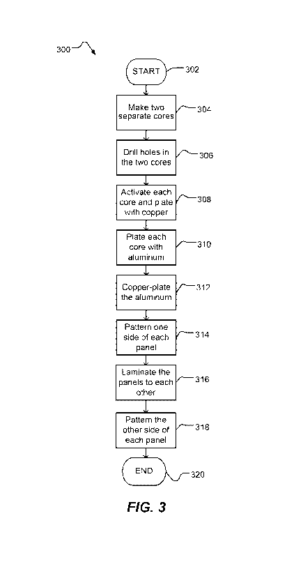
Figure 3 is a flow chart illustrating a method 300 for fabricating a
multilayer superconducting printed circuit board, according to one illustrated
implementation of the present disclosure. Method 300 includes acts 302-320,
though those skilled in the art will appreciate that in alternative
implementations
certain acts may be omitted and/or additional acts may be added. Those skilled
in the art will appreciate that the order of the acts is shown for exemplary
purposes only and may change in alternative implementations.
33
CA 03045487 2019-05-29
WO 2018/106942 PCT/US2017/065152
At 302, the method starts. At 304, two separate cores comprising
an electrically insulative substrate are made. At 306, one or more holes are
drilled or formed in each of the two cores. At 308, each core is activated,
and
the electrically insulative substrate is copper-plated. At 310, each copper-
plated core is plated with aluminum. At 312, the aluminum-plated core is
plated
with copper to form two panels each comprising a bimetal foil of Cu/Al/Cu.
Other implementations may use other suitable bimetal foils.
At 314, one side of each core is patterned. This side becomes an
inner layer of the multilayer PCB. At 316, the two panels are laminated to
each
other to form a multilayer superconducting PCB. At 318, the other side (i.e.,
the
outer side) of each panel is patterned. At 320, the method ends.
Method 300 is described in more detail above, and in reference to
Figures 2A, 2B, 2C, 2D, and 2E.
Figure 4 is a set of two cross-sectional views of a multilayer PCB
400, according to one illustrated implementation of the present disclosure.
PCB
400 comprises two cores 402 and 404. Core 402 comprises a via 406, and
core 404 comprises a via 408. Vias 406 and 408 may be superconducting vias.
Core 402 further comprises a trace 410, and core 404 further comprises a trace
412. Traces 410 and 412 may be superconducting traces. Traces 410 and 412
may comprise a superconducting metal such as aluminum for example.
As shown in Figure 4, traces 410 and 412 can be joined by a
segment of superconducting metal 414. In one implementation,
superconducting metal 414 includes tin. Superconducting metal 414 can
provide a superconducting electrical coupling between traces 410 and 412.
Superconducting metal 414 can provide a mechanical coupling of cores 402
and 404 to form a multilayer PCB.
In one implementation, superconducting vias 406 and 408, traces
410 and 412, and the segment of superconducting metal 414 form a
superconducting electrical communicative path.
In some embodiments of the present systems, methods and
apparatus, it may be advantageous to secure a distinct plug or core of
material
34
CA 03045487 2019-05-29
WO 2018/106942 PCT/US2017/065152
inside a superconducting via. In some applications, the superconducting metal
that plates the inner surface of a superconducting via may fragment or detach
from the inner surface of the via. The likelihood of this fragmentation may be
reduced by inserting a distinct plug or core inside the superconducting via.
For
example, a piece of wire, such as copper wire, may be inserted inside a
superconducting via. This wire may be secured in place, for example, by a
solder connection and/or by bending the ends of the wire that may protrude
from the superconducting via. Placing such a wire in a superconducting via
may help to protect the surface of the superconducting via and hold the
superconducting plating in place.
According to the present state of the art, a superconducting
material may generally only act as a superconductor if it is cooled below a
critical temperature that is characteristic of the specific material in
question. For
this reason, those of skill in the art will appreciate that a system that
implements
superconducting devices may implicitly include a system for cooling the
superconducting materials in the system. Systems and methods for such
cooling are well known in the art. A dilution refrigerator is an example of a
system that is commonly implemented for cooling a superconducting material to
a temperature at which the superconducting material may act as a
superconductor. In common practice, the cooling process in a dilution
refrigerator may use a mixture of at least two isotopes of helium (such as
helium-3 and helium-4). Full details on the operation of typical dilution
refrigerators may be found in F. Pobell, Matter and Methods at Low
Temperatures, Springer-Verlag Second Edition, 1996, pp. 120-156. However,
those of skill in the art will appreciate that the present systems, methods
and
apparatus are not limited to applications involving dilution refrigerators,
but
rather may be applied using any type of cooling system.
The above description of illustrated embodiments, including what
is described in the Abstract, is not intended to be exhaustive or to limit the
embodiments to the precise forms disclosed. Although specific embodiments of
and examples are described herein for illustrative purposes, various
equivalent
CA 03045487 2019-05-29
WO 2018/106942
PCT/US2017/065152
modifications can be made without departing from the spirit and scope of the
disclosure, as will be recognized by those skilled in the relevant art. The
teachings provided herein of the various embodiments can be applied to
multilayer superconducting PCB systems, methods and apparatus, not
necessarily the exemplary multilayer superconducting PCB systems, methods,
and apparatus generally described above.
The various embodiments described above can be combined to
provide further embodiments. All of the U.S. patents, U.S. patent application
publications, U.S. patent applications, foreign patents, foreign patent
applications and non-patent publications referred to in this specification
and/or
listed in the Application Data Sheet, including but not limited to US
Provisional
Patent Application Serial No. 60/979,031, filed October 10, 2007, entitled
"Systems, Methods and Apparatus for Multilayer Superconducting Printed
Circuit Boards", US Patent Application Serial No. 12/016,801, US Patent
Application Serial No. 12/016,709, United States Patent 8,315,678 entitled
"Systems, Methods, and Apparatus for Multilayer Superconducting Printed
Circuit Boards", US Provisional Patent Application Serial No. 60/881,358,
filed
January 18, 2007, entitled "Input/Output Systems and Devices for Use with
Superconducting Based Computing Systems", United States Patent 8,441,329
entitled "Input/Output Systems and Devices for Use with Superconducting
Based Computing Systems", US Provisional Patent Application Serial No.
62/431,333, filed December 7, 2016, entitled "Multilayer Superconducting
Printed Circuit Board Related Systems, Methods, And Apparatus" and United
States Patent 8,008,991 entitled "Systems, Methods and Apparatus for
Electrical Filters" are incorporated herein by reference, in their entirety.
Aspects of the embodiments can be modified, if necessary, to employ systems,
circuits and concepts of the various patents, applications and publications to
provide yet further embodiments.
These and other changes can be made to the embodiments in
light of the above-detailed description. In general, in the following claims,
the
terms used should not be construed to limit the claims to the specific
36
CA 03045487 2019-05-29
WO 2018/106942
PCT/US2017/065152
embodiments disclosed in the specification and the claims, but should be
construed to include all possible embodiments along with the full scope of
equivalents to which such claims are entitled. Accordingly, the claims are not
limited by the disclosure.
37