Note: Descriptions are shown in the official language in which they were submitted.
CA 03045981 2019-06-03
WO 2018/135223 PCT/JP2017/045752
Description
Title of Invention: SPECTROMETER, ANALYSIS EQUIPMENT,
AND WAVELENGTH-VARIABLE LIGHT SOURCE
Technical Field
[0001] The present invention relates to a spectrometer, an analysis
equipment, and a
wavelength-variable light source.
Background Art
[0002] What is called a spectrometer, which is for dispersing light of
measurement on a
wavelength basis, so as to obtain a spectroscopic spectrum of each of the
wavelengths,
is conventionally known in the art.
[0003] Note that a general spectrometer is configured with a concave
diffraction grating for
dispersing incident light of measurement into light with multiple wavelengths
and with
an array sensor that is capable of detecting each of the light with the
multiple
wavelengths (see PLT 1 as shown below, for example). For example, a silicon
(Si)
photodiode, an InGaAs (indium gallium arsenide) photodiode, etc., may be
employed
for an array sensor.
Citation List
Patent Literature
[0004] [PLT 1] Japanese Unexamined Patent Application Publication No. 2015-
148485
Summary of Invention
Technical Problem
[0005] However, conventionally, there has been an issue that a small-scale
and inexpensive
spectrometer cannot be provided because an array sensor employed for a
spectrometer
is large-scale and expensive.
[0006] As a solution to the above-described issue relating to the
conventional technique, the
object of the present invention is to enable to provide a small-scale and
inexpensive
spectrometer.
Solution to Problem
[0007] As a solution to the above-described issue, one aspect of the
present invention
provides a spectrometer including: a light incidence unit configured to allow
incidence
of light from outside; a diffraction grating configured to disperse, according
to
wavelength, the light that is incident through the light incidence unit; and a
reflection
unit including a reflection surface for reflecting the light that has been
dispersed
according to wavelength by the diffraction grating. Tilt of the reflection
surface is
changeable.
85316696
2
Advantageous Effects of Invention
[0008] According to the present invention, a small-scale and inexpensive
spectrometer
can be provided.
[0008a] According to one aspect of the present invention, there is provided
a
spectrometer comprising: a light incidence unit configured to allow incidence
of
light from outside; a diffraction grating configured to disperse, according to
wavelength, the light that is incident through the light incidence unit; a
reflection
unit including a reflection surface for reflecting the light that has been
dispersed
according to wavelength by the diffraction grating; and a light output unit
including
a light passage unit through which the light, which is reflected by the
reflection
unit, passes, wherein the reflection unit is configured to rotate about a
predetermined rotation axis, and the tilt of the reflection surface changes in
accordance with the rotation movement of the reflection unit.
Brief Description of Drawings
[0009] [fig. 1] FIG. 1 is a conceptual view illustrating a configuration of
a spectrometer
according to a first embodiment of the present invention;
[fig. 2] FIG. 2 is a schematic view of a configuration of a light reflection
unit
according to the first embodiment of the present invention;
[fig. 3] FIG. 3 is a cross sectional view taken along Line A-A' of the light
reflection
unit illustrated in FIG. 2;
[fig. 4] FIG. 4 is a cross sectional view taken along Line B-B' of the light
reflection
unit illustrated in FIG. 2;
[fig. 5] FIG. 5 is a schematic view illustrating a first configuration example
of a
concave diffraction grating according to the first embodiment of the present
invention;
[fig. 6] FIG. 6 is a schematic view illustrating a second configuration
example of
the concave diffraction grating according to the first embodiment of the
present
invention;
Date Recue/Date Received 2020-10-30
85316696
2a
[fig. 7] FIG. 7 is a schematic view illustrating a third configuration example
of the
concave diffraction grating according to the first embodiment of the present
invention;
[fig. 8] FIG. 8 is a conceptual view illustrating a first variation example of
a
configuration of the spectrometer according the first embodiment of the
present
invention;
[fig. 9] FIG. 9 is a conceptual view illustrating a second variation example
of a
configuration of the spectrometer according to the first embodiment of the
present
invention;
[fig. 10] FIG. 10 is a conceptual view illustrating a third variation example
of a
configuration of the spectrometer according to the first embodiment of the
present
invention;
[fig. 11] FIG. 11 is a conceptual view illustrating a fourth variation example
of a
configuration of the spectrometer according to the first embodiment of the
present
invention;
[fig. 12] FIG. 12 is a conceptual view illustrating a fifth variation example
of a
configuration of the spectrometer according to the first embodiment of the
present
invention;
[fig. 13] FIG. 13 is a conceptual view illustrating a sixth variation example
of a
configuration of the spectrometer according to the first embodiment of the
present
invention;
[fig. 14] FIG. 14 is a conceptual view illustrating a seventh variation
example of a
configuration of the spectrometer according to the first embodiment of the
present
Date Recue/Date Received 2020-10-30
3
CA 03045981 2019-06-03
WO 2018/135223 PCT/JP2017/045752
invention;
[fig.151FIG. 15 is a conceptual view illustrating an eighth variation example
of a con-
figuration of the spectrometer according to the first embodiment of the
present
invention;
lfig.161FIG. 16 is a conceptual view illustrating a configuration of a
spectrometer
according to a second embodiment of the present invention;
[fig.171FIG. 17 is a conceptual view illustrating a configuration (i.e., a
first example)
of a specific wavelength detecting device according to the second embodiment
of the
present invention;
lfig.18lFIG. 18 is a conceptual view illustrating a configuration (i.e., a
second
example) of the specific wavelength detecting device according to the second
em-
bodiment of the present invention;
lfig.191FIG. 19 is a drawing illustrating an example of an output signal of
the specific
wavelength detecting device according to the second embodiment of the present
invention;
[fig.201FIG. 20 is a drawing illustrating an example of an output signal of
the specific
wavelength detecting device according to the second embodiment of the present
invention;
Ifig.211FIG. 21 is a drawing illustrating an example of an output signal of
the specific
wavelength detecting device according to the second embodiment of the present
invention;
lfig.221FIG. 22 is a drawing illustrating an example of a time waveform for
deflection
angle of a movable light reflection part according to the second embodiment of
the
present invention;
[fig.231FIG. 23 is a conceptual view illustrating a first variation example of
a con-
figuration of the spectrometer according to the second embodiment of the
present
invention;
[fig.241FIG. 24 is a conceptual view illustrating a second variation example
of a con-
figuration of the spectrometer according to the second embodiment of the
present
invention;
lfig.251FIG. 25 is a conceptual view illustrating a third variation example of
a con-
figuration of the spectrometer according to the second embodiment of the
present
invention;
Ifig.261FIG. 26 is a conceptual view illustrating a fourth variation example
of a con-
figuration of the spectrometer according to the second embodiment of the
present
invention;
[fig.271FIG. 27 is a conceptual view illustrating another configuration of the
spec-
trometer according to the second embodiment of the present invention; and
4
CA 03045981 2019-06-03
WO 2018/135223 PCT/JP2017/045752
[fig.281FIG. 28 is a conceptual view illustrating a configuration of a
spectroscopic
measurement apparatus by use of the spectrometer according to the first
embodiment
of the present invention.
Description of Embodiments
[0010] <First Embodiment>
[0011] The following description explains the first embodiment of the
present invention,
with reference to the accompanying drawings.
[0012] (Configuration of a Spectrometer 10A)
[0013] FIG. 1 is a conceptual view illustrating a configuration of a
spectrometer 10A
according to the first embodiment of the present invention. The spectrometer
10A il-
lustrated in FIG. 1 is an example of a "spectrometer" in the present
invention. The
spectrometer 10A is configured with a light incidence part 1, a concave
diffraction
grating 2, a movable light reflection part 3, a light output part 4, a
substrate 5, and a
substrate 6.
100141 The light incidence part 1 is an example of a "light incidence unit"
in the present
invention. The light incidence part 1 includes a light passage part la. The
light
incidence part 1 allows externally emitted light to pass through the light
passage part
la, such that the light is incident to the spectrometer 10A. The light passage
part la is,
for example, in a pinhole-shape, a slit-shape, etc. The light incidence part 1
is provided
for the purpose of deciding an incidence position of light, improving
wavelength
resolution, etc.
100151 The concave diffraction grating 2 is an example of a "diffraction
grating'' in the
present invention. The concave diffraction grating 2 is formed on the
substrate 5. The
concave diffraction grating 2 causes wavelength dispersion of light that is
incident to
the spectrometer 10A from the light incidence part 1. The light (i.e.,
diffracted light) on
which wavelength dispersion is performed by the concave diffraction grating 2
is
reflected towards the movable light reflection part 3. Material for the
substrate 5 may
be, for example, semiconductor, glass, metal, resin, etc., but is not limited
to such
material. Note that the concave diffraction grating 2 may be formed directly
on the
substrate 5 and may be formed on a thin film layer (e.g., a resin layer, etc.)
formed on
the substrate 5.
[0016] The movable light reflection part 3 is an example of a "reflection
unit" in the present
embodiment. The movable light reflection part 3 is arranged inside an opening
part 6a
of the substrate 6 in the same plane of the substrate 6. Together with the
substrate 6,
the movable light reflection part 3 configures a light reflection unit 11. The
movable
light reflection part 3 reflects diffracted light, which has been dispersed by
the concave
diffraction grating 2, towards the light output part 4. The movable light
reflection part
5
CA 03045981 2019-06-03
WO 2018/135223 PCT/JP2017/045752
3 includes a rotation axis 3a. The movable light reflection part 3 is
configured to rotate
on the rotation axis 3a, such that tilt of the reflection surface for
reflecting diffracted
light can be changed. Material for the substrate 6 may be, for example,
semiconductor,
glass, metal, resin, etc., but is not limited to such material. However, in a
case of using
semiconductor as material for the substrate 6, an extremely thin and small-
scale
movable light reflection part 3 can be formed, by means of a semiconductor
process, a
microelectromechanical system (MEMS) process, etc. Furthermore, in the case of
using semiconductor as material for the substrate 6, a driving element by
means of
piezoelectric actuation, electrostatic actuation, electromagnetic actuation,
etc., can be
monolithically formed on the substrate 6. Therefore, the spectrometer 10A can
be
down-scaled because the movable light reflection part 3 can be driven without
an
external driving device such as a motor.
[0017] The light output part 4 is an example of a "light output unit" in
the present invention.
The light output part 4 includes a light passage part 4a. The light output
part 4 allows
diffracted light that has been reflected by the movable light reflection part
3 to pass
through the light passage part 4a at a focal point, such that the diffracted
light is ex-
ternally output. The light passage part 4a is, for example, in a pinhole-
shape, a slit-
shape. etc. The light output part 4 is provided for the purpose of deciding an
output
position of diffracted light, improving wavelength resolution, etc.
[0018] Note that each of the light incidence part 1 and the light output
part 4 may be formed
on a substrate. In the above case, material for the substrates may be, for
example, semi-
conductor, glass, metal, resin, etc., but is not limited to such material.
However, in a
case of using semiconductor as material for the substrates, the light
incidence part 1
and the light output part 4 can be formed with a high degree of accuracy and
at a low
cost, by means of a semiconductor process, an MEMS process, etc.
[0019] Additionally, in the spectrometer 10A, each of the above-described
constituent
elements is arranged at a predetermined position and fixed to the structure,
supports,
etc., to maintain a predetermined angle, as illustrated in FIG. 1.
[0020] (Configuration of the Light Reflection Unit 11)
[0021] The following description explains a specific configuration of the
light reflection unit
11, with reference to FIGS. 2 through 4. FIG. 2 is a schematic view of a
configuration
of the light reflection unit 11 according to the first embodiment of the
present
invention. As illustrated in FIG. 2, the light reflection unit 11 is
configured with a
movable light reflection part 3, a substrate 6, a driving circuit 7 (i.e. an
example of a
"driving unit" in the present invention), and a beam part 8. The movable light
re-
flection part 3 is arranged inside an opening part 6a of the substrate 6 in
the same plane
of the substrate 6. The opening part 6a is formed by means of a MEMS process
such as
an isotropic deep etching. The movable light reflection part 3 is supported by
the beam
6
CA 03045981 2019-06-03
WO 2018/135223 PCT/JP2017/045752
part 8 with respect to both an end part of the rotation axis 3a and the other
end part of
the rotation axis 3a.
[0022] Furthermore. in the example of FIG. 2, the movable light reflection
part 3 is
configured with a thin film part 3b and a reflection member 3c, which is
superimposed
on a reflection surface of the thin film part 3b. The reflection member 3c is
provided
for the purpose of improving the reflection rate of the movable light
reflection part 3.
As the thin film part 3b, a thin film silicon (Si) layer on a silicon-on-
insulator (SOI)
substrate, etc., may be employed, for example. Furthermore, as the reflection
member
3c, metal material such as aluminum (Al). silver (Ag), gold (Au), or platinum
(Pt) may
be used, for example.
[0023] FIG. 3 is a cross sectional view taken along Line A-A' of the light
reflection unit 11
illustrated in FIG. 2. In the example of FIG. 3, the beam part 8 is configured
with a thin
film part 8a, an electrode 8b, a piezoelectric film 8d, and an electrode 8c,
which are su-
perimposed in the said order from top (i.e., the positive direction of Z-axis)
to bottom
of FIG. 3. Having the above-described configuration, the beam part 8 is able
to
function as an actuator for driving the movable light reflection part 3 to
rotate, when
the driving circuit 7 (cf. FIG. 2) applies a voltage to the piezoelectric film
8d via the
electrodes 8b and 8c. For example, to externally output diffracted light with
a desired
wavelength, the movable light reflection part 3 is required to be tilted at a
prede-
termined angle that corresponds to the wavelength. For example, the driving
circuit 7
applies a predetermined voltage to the piezoelectric film 8d. Alternatively,
the driving
circuit 7 applies a voltage to the piezoelectric film 8d, based on a feedback
of an angle
detected by a tilt sensor, which is provided in the movable light reflection
part 3. In the
above ways, the movable light reflection part 3 can be tilted at a
predetermined angle.
Note that, the driving method for the movable light reflection part 3 is not
limited to
the piezoelectric actuation and may be another driving method such as
electrostatic
actuation or electromagnetic actuation.
[0024] FIG. 4 is a cross sectional view taken along Line B-B of the light
reflection unit 11
illustrated in FIG. 2. As illustrated in FIG. 4, the movable light reflection
part 3 is
configured to rotate on the rotation axis 3a in the clockwise or
counterclockwise
direction when being driven by the beam part 8 as explained with reference to
FIG. 3,
such that tilt of the reflection surface for reflecting diffracted light can
be changed.
[0025] (Configuration Examples of the Concave Diffraction Grating 2)
[0026] Next, the following description explains specific configurations of
the concave
diffraction grating 2, with reference to FIGS. 5 through 7.
[0027] FIG. 5 is a schematic view illustrating a first configuration
example of the concave
diffraction grating 2 according to the first embodiment of the present
invention. In the
example of FIG. 5, the concave diffraction grating 2 is configured with a
resin layer 14
7
CA 03045981 2019-06-03
WO 2018/135223 PCT/JP2017/045752
and a reflection member 15. Specifically, a concave surface is formed on a top
surface
of the substrate 5. Further, the resin layer 14, which is in a shape of a thin
film, is
formed on the concave surface. Furthermore, a diffraction grating is formed on
the
resin layer 14. Additionally, the reflection member 15 using metal material
such as Al,
Ag, Au, or Pt is formed on a surface of the diffraction grating for the
purpose of
improving the reflection rate.
[0028] For example, in a case where a Si substrate is employed as the
substrate 5, a concave
surface can be formed on the substrate 5 by forming a concave-surface-forming
pattern
on a resist applied on the substrate 5 by means of grayscale masking,
nanoimprint
technology, etc., and then performing dry-etching, etc. Furthermore, a
diffraction
grating can be formed on the resin layer 14 by forming the resin layer 14 on
the
concave surface of the substrate 5 and then transferring a template for a
concave
diffraction grating, which is prepared in another process, onto the resin
layer 14 and
curing the resin layer 14.
[0029] FIG. 6 is a schematic view illustrating a second configuration
example of the
concave diffraction grating 2 according to the first embodiment of the present
invention. In the example of FIG. 6, the concave diffraction grating 2 is
configured
with a reflection member 15. Specifically, a concave surface is formed on a
top surface
of the substrate 5. Further, a diffraction grating is formed on the concave
surface. Ad-
ditionally, the reflection member 15 using metal material such as Al, Ag, Au,
or Pt is
formed on a surface of the diffraction grating for the purpose of improving
the re-
flection rate. For example, the diffraction grating can be formed on the
concave surface
of the substrate 5 by applying a resist on the concave surface of the
substrate 5, then
forming a grating pattern on the resist by means of an interference exposure
method,
etc., and then performing dry-etching, etc.
[0030] FIG. 7 is a schematic view illustrating a third configuration
example of the concave
diffraction grating 2 according to the first embodiment of the present
invention. In the
example of FIG. 7, the concave diffraction grating 2 is configured with a
resin layer 14
and a reflection member 15. Specifically, a resin layer 14 is formed on a top
surface
(i.e., a flat surface) of the substrate 5. A concave surface is formed on a
top surface of
the resin layer 14 and a diffraction grating is formed on the concave surface.
Fur-
thermore, a reflection member 15 using metal material such as Al, Ag, Au, or
Pt is
formed on a surface of the diffraction grating for the purpose of improving
the re-
flection rate. For example, the diffraction grating can be formed on the resin
layer 14
by forming the resin layer 14 on the top surface (i.e., the flat surface) of
the substrate 5
and then transferring a template for a concave diffraction grating, which is
prepared in
another process, onto the resin layer 14 and curing the resin layer 14. The
process for
forming the configuration illustrated in FIG. 7 can be simple because a
process for
8
CA 03045981 2019-06-03
WO 2018/135223 PCT/JP2017/045752
forming a concave surface on the substrate 5 is not necessary.
[0031] Note that, regarding each of the concave diffraction gratings 2 as
illustrated in
FIGS.5 through 7, the cross section of a groove portion of a diffraction
grating may be
in a rectangular shape, a sinusoidal shape, a sawtooth-wave shape, etc.
[0032] Further, it is possible that each of the concave diffraction
gratings 2 as illustrated in
FIGS.5 through 7 may be configured without the reflection member 15. Further,
the
configuration of a concave diffraction grating 2 is not limited to as
illustrated in FIGS.
through 7. That is to say, the concave diffraction grating 2 may have a
configuration
other than as illustrated in FIGS. 5 through 7, as long as the concave
diffraction grating
2 has a similar function of wavelength dispersion. Furthermore, in a case
where
parallel light is incident from the light incidence part 1, a flat concave
diffraction
grating may be employed, instead of a concave diffraction grating 2, for
achieving the
similar function of wavelength dispersion. In the above case, a complex device
con-
figuration (e.g., a collimating optical system for forming light into parallel
light before
and after being incident to a flat diffraction grating), which is required in
a case of
employing a configuration for changing tilt of a flat diffraction grating, is
not
necessary.
[0033] (Function and Effect of a Spectrometer 10A)
[0034] A spectrometer 10A according to the present embodiment, which is
configured as
described above, drives the movable light reflection part 3 to change tilt of
the re-
flection surface of the movable light reflection part 3, such that a
wavelength of
diffracted light, which is externally output from the light output part 4, can
be changed.
Specifically, the focal length of diffracted light, on which wavelength
dispersion is
performed by the concave diffraction grating 2, differs based on each
wavelength.
Hence, a spectrometer 10A changes tilt of the reflection surface of the
movable light
reflection part 3. such that the position of the light passage part 4a of the
light output
part 4 matches a position that corresponds a focal length of diffracted light
with a
desired wavelength. In the above way, diffracted light with a desired
wavelength is
output from the light passage part 4a of the light output part 4, as
illustrated in FIG. 1.
Note that dashed lines of FIG. 1 schematically indicate a light path for light
with a
specific wavelength. In other words, in FIG. 1, a situation of setting tilt of
the re-
flection surface of the movable light reflection part 3 so as to output
diffracted light
with a predetermined wavelength is illustrated.
[0035] As described above, a spectrometer 10A according to the present
invention adjusts
tilt of the reflection surface of the movable light reflection part 3, so as
to output
diffracted light with a desired wavelength through the light passage part 4a
of the light
output part 4. Therefore, in a case of a spectrometer 10A according to the
present em-
bodiment, a spectroscopic spectrum of diffracted light with desired
wavelengths can be
9
CA 03045981 2019-06-03
WO 2018/135223 PCT/JP2017/045752
obtained by an externally-installed single light sensor (i.e., a light
detecting unit as
described below). In other words, in a case of a spectrometer 10A according to
the
present invention, a spectroscopic spectrum of diffracted light with various
wavelengths can be obtained without an array sensor, which is large-scale and
expensive. Therefore, in a case of a spectrometer 10A according to the present
em-
bodiment, it is possible to provide a small-scale and inexpensive
spectrometer.
[0036] Furthermore. in a case of a spectrometer 10A of the present
embodiment, diffracted
light with a desired wavelength is output through the light passage part 4a of
the light
output part 4 by changing tilt of the reflection surface of the movable light
reflection
part 3 without changing tilt of the concave diffraction grating 2. Therefore,
in a case of
a spectrometer 10A according to the present embodiment, a complex device con-
figuration (e.g., a configuration for accommodating change in the incident
angle of
light to the concave diffraction grating 2) that is required in a case of
employing a con-
figuration for changing tilt of a concave diffraction grating 2 is not
necessary.
Therefore, in a case of a spectrometer 10A according to the present
embodiment,
diffracted light with a desired wavelength can be output through the light
passage part
4a of the light output part 4 with a relatively simple configuration.
[0037] Furthermore. in a case of a spectrometer 10A according to the
present embodiment,
incident light is reflected twice: reflection by the concave diffraction
grating 2 and re-
flection by the movable light reflection part 3. Therefore, in a case of a
spectrometer
10A according to the present embodiment, a configuration can be simplified and
decrease in light intensity due to reflection loss can be prevented, in
comparison with a
configuration such as Japanese Unexamined Patent Application Publication No.
2015-148485, where light is reflected three times or more.
[0038] Note that a spectrometer 10A according to the present embodiment may
be employed
for configuring a spectroscopic measurement apparatus, in combination with at
least a
light detecting device for detecting diffracted light output through the light
passage
part 4a of the light output part 4. Here, the light detecting device may be
one having a
single light sensor. Further, a spectrometer 10A according to the present
embodiment
may be employed for configuring a monochromator, in combination with at least
an
optical fiber for guiding diffracted light output through the light passage
part 4a of the
light output part 4.
[0039] (Variation Examples of the Configuration of a Spectrometer)
[0040] The following description explains variation examples of the
configuration of a spec-
trometer. Note that, in the following explanation of each variation example,
difference
from the previously-explained spectrometer is explained. Further, in each
variation
example, each constituent element having the same function as a previously-
explained
constituent element is assigned the same reference sign, so as to omit
explanation of
10
CA 03045981 2019-06-03
WO 2018/135223 PCT/JP2017/045752
the previously-explained constituent element. Further, the operational
mechanism, etc.,
of a spectrometer is the same as previously explained, and therefore the
explanation is
omitted in each variation example.
[0041] (First Variation Example)
[0042] FIG. 8 is a conceptual view illustrating a first variation example
of a configuration of
a spectrometer according to the first embodiment of the present embodiment.
With
respect to a spectrometer 10B illustrated in FIG. 8, a light incidence part 1
and a
movable light reflection part 3 are formed on a single substrate 6.
Furthermore, with
respect to the spectrometer 10B, a light output part 4 and a concave
diffraction grating
2 are formed on a single substrate 5. For example, in a case of employing Si
substrates
as the substrates 5 and 6, the light incidence part 1 and the light output
part 4 are in-
tegrally formed on the substrates 6 and 5, respectively, by means of a
semiconductor
process, an MEMS process, etc.
[0043] In a case of the spectrometer 10B, the light incidence part 1 and
the light output part
4 can be formed on the substrates 6 and 5, respectively, with a high degree of
accuracy
by means of a semiconductor process. That is to say, in a case of the
spectrometer 10B,
adjustment for overall alignment is simplified because adjustment for
alignment of the
light incidence part 1 and the movable light reflection part 3 and adjustment
for
alignment between the light output part 4 and the concave diffraction grating
2 are not
required. Furthermore, the spectrometer 10B may be configured without any
parts of
the structure, supports, etc., intervening between the light incidence part 1
and the
movable light reflection part 3 and between the light output part 4 and the
concave
diffraction grating 2. Therefore, in a case of the spectrometer 10B, distances
between
the light incidence part 1 and the movable light reflection part 3 and between
the light
output part 4 and the concave diffraction grating 2 can be shorter, and
therefore a
smaller-scale spectrometer can be achieved.
[0044] (Second Variation Example)
[0045] FIG. 9 is a conceptual view illustrating a second variation example
of a configuration
of a spectrometer according to the first embodiment of the present invention.
With
respect to a spectrometer 10C illustrated in FIG. 9, a light incidence part 1
and a light
output part 4 are formed on a single substrate 16.
[0046] In a case of the spectrometer 10C, the light incidence part 1 and
the light output part
4 can be formed on the substrate 16 with a high degree of accuracy, by means
of a
semiconductor process. That is to say, in a case of the spectrometer 10C,
adjustment
for overall alignment is simplified because adjustment for alignment between
the light
incidence part 1 and the light output part 4 is not required.
[0047] (Third Variation Example)
1100481 FIG. 10 is a conceptual view illustrating a third variation example
of a configuration
11
CA 03045981 2019-06-03
WO 2018/135223 PCT/JP2017/045752
of a spectrometer according to the first embodiment of the present invention.
In
comparison with the spectrometer 10B illustrated in FIG. 8, a spectrometer 10D
il-
lustrated in FIG. 10 has a configuration that further includes a pair of
spacers 17, one
of which is on the right and the other of which is on the left, between the
substrate 5
and the substrate 6. The substrate 5 is an example of a "second substrate" in
the present
invention. The substrate 6 is an example of a "first substrate" of the present
invention.
Each of the spacers 17 is an example of an "intervening member" in the present
invention. Each of the substrates 5 and 6 is joined to the spacers 17. Each of
the
spacers 17 may be in a shape of a pole, a plate, etc. The distance between the
substrate
and the substrate 6 is adjusted by thickness of the spacers 17 into a proper
distance
for obtaining desired spectroscopic characteristics.
[0049] In a case of the spectrometer 10D, the distance between the
substrate 5 and the
substrate 6 is adjusted by thickness of the spacers 17 into a proper distance
for
obtaining desired spectroscopic characteristics. Therefore, in a case of the
spectrometer
10D, adjustment for alignment between the substrate 5 and the substrate 6 is
not
required. Note that each of the spacers 17 of the spectrometer 10D may be a
substrate.
In this case, each of the spacers 17 can be formed with a high degree of
accuracy, by
means of a semiconductor process. Furthermore, multiple spacers 17 can be fon-
ned at
once on a wafer with a high degree of accuracy. Therefore, a spectrometer with
a small
degree of variability and a low cost can be achieved.
[0050] (Fourth Variation Example)
[0051] FIG. 11 is a conceptual view illustrating a fourth variation example
of a con-
figuration of a spectrometer according to the first embodiment of the present
invention.
A spectrometer 10E illustrated in FIG. 11 is different from the spectrometer
10D il-
lustrated in FIG. 10 in terms of the point that a light output part 4 is
formed on the right
(i.e., at a position in the positive direction of Y-axis in FIG. 11) of the
concave
diffraction grating 2 on the substrate 5. The concave diffraction grating 2 of
the spec-
trometer 10E has a wider grating pitch, comparing with the spectrometer 10D il-
lustrated in FIG. 10. Accordingly, the diffraction angle of the concave
diffraction
grating 2 is changed, and therefore the position of the light output part 4 of
the spec-
trometer 10E is modified. In a case of the spectrometer 10E, as the concave
diffraction
grating 2 has a wider grating pitch in comparison with the spectrometer 10D,
the
concave diffraction grating 2 can be easily manufactured. Therefore, in a case
of the
spectrometer 10E, a spectrometer with a small degree of manufactural
variability and a
low cost can be achieved in comparison with a case of the spectrometer 10D.
[0052] (Fifth Variation Example)
[0053] FIG. 12 is a conceptual view illustrating a fifth variation example
of a configuration
of a spectrometer according to the first embodiment of the present invention.
A spec-
12
CA 03045981 2019-06-03
WO 2018/135223 PCT/JP2017/045752
trometer 1OF illustrated in FIG. 12 is different from the spectrometer 10D
illustrated in
FIG. 10 in terms of the point that the concave diffraction grating 2 is
arranged at an
angle with respect to the substrate 5, facing towards the light incidence part
1 (i.e., in
the negative direction of the Y-axis in FIG. 12), such that a normal with
respect to the
center of the concave diffraction grating 2 on the substrate 5 is not at right
angle to the
substrate surface of the substrate 5.
[0054] In a case of the spectrometer 10F, which has the above-described
configuration, the
incident angle of diffracted light to the movable light reflection part 3 is
adjusted
through the changed tilt of the concave diffraction grating 2, such that
required de-
flection angles of the movable light reflection part 3 become equal in the
positive and
the negative direction. Therefore, in a case of the spectrometer 10F, the same
range of
wavelengths can be measured with smaller deflection angles of the movable
light re-
flection part 3. Accordingly, in a case of the spectrometer 10F, the movable
light re-
flection part 3 can be driven with smaller driving force. Therefore, in a case
of the
spectrometer 10F, constituent elements (e.g., a driving element, a driving
circuit, a
power source, etc.) required for driving of the movable light reflection part
3 can be
smaller, which enables a smaller-scale spectrometer to be achieved with a
lower cost.
Furthermore, in a case of a spectrometer 10F, as the amount of turn with
respect to the
beam part 8 supporting the movable light reflection part 3 is decreased, it is
possible to
reduce stress imposed on the beam part 8. Therefore, in a case of the
spectrometer 10F,
stability, reliability, etc., with respect to rotation angle of the movable
light reflection
part 3 can be improved.
[0055] (Sixth Variation Example)
[0056] FIG. 13 is a conceptual view illustrating a sixth variation example
of a configuration
of a spectrometer according to the first embodiment of the present invention.
A spec-
trometer 10G illustrated in FIG. 13 is different from the spectrometer 10D
illustrated in
FIG. 10 in terms of the point that a spacer 17 on the left (i.e., at a
position in the
negative direction of the Y-axis in FIG. 10) is changed to a substrate 19 and
that a light
incidence part 1 and a light output part 4 are formed on the substrate 19.
[0057] The substrate 19 is an example of a "third substrate" in the present
invention. The
substrate 19 is arranged between the substrate 5 and the substrate 6 such that
the
substrate 19 is non-parallel and is vertical to the substrate 5 and the
substrate 6. Fur-
thermore, each of the substrate 5 and the substrate 6 is joined to the
substrate 19.
Material for the substrate 19 may be, for example, semiconductor, glass,
metal, resin,
etc., but is not limited to such material. However, in a case of using
semiconductor as
material for the substrate 19, an extremely thin and small-scale light
incidence part 1
and light output part 4 can be formed by means of a semiconductor process, a
MEMS
process, etc.
13
CA 03045981 2019-06-03
WO 2018/135223 PCT/JP2017/045752
[0058] In a case of the spectrometer 10G, the light incidence part 1 and
the light output part
4 can be formed on the substrate 19 with a high degree of positional accuracy
by
means of a semiconductor process. That is to say, in a case of the
spectrometer 10G,
adjustment for overall alignment is simplified because adjustment for
alignment
between the light incidence part 1 and the light output part 4 is not
required. Note that,
with respect to the spectrometer 10G, the light incidence part I can be formed
on the
substrate 6 and the light output part 4 can be formed on the substrate 19.
Contrarily,
with respect to the spectrometer 10G, the light incidence part I can be formed
on the
substrate 19 and the light output part 4 can be formed on the substrate 5.
[0059] (Seventh and Eighth Variation Examples)
[0060] FIG. 14 is a conceptual view illustrating a seventh variation
example of a con-
figuration of a spectrometer according to the first embodiment of the present
invention.
FIG. 15 is a conceptual view illustrating an eighth variation example of a
configuration
of a spectrometer according to the first embodiment of the present invention.
A spec-
trometer 10H illustrated in FIG. 14 is different from the spectrometer 10A
illustrated in
FIG. 1 in terms of the point that a light detecting part 18 is provided at the
location of
the light output part 4, instead of the light output part 4. A spectrometer
101 illustrated
in FIG. 15 is different from the spectrometer 10B illustrated in FIG. 8 in
terms of the
point that a light detecting part 18 is provided at the location of the light
output part 4,
instead of the light output part 4. The light detecting part 18 of each of the
spec-
trometers 10H and 101 is an example of a "light detecting unit" in the present
invention.
[0061] In a case of the spectrometer 10H or 101, a smaller-scale
spectrometer can be
achieved because there is no need for externally providing the light detecting
part 18.
Note that a reception surface of the light detecting part 18 may be formed in
the same
shape (e.g., a pinhole-shape, a slit-shape, etc.) as the light passage part 4a
of the light
output part 4. Further, the light detecting part 18 may include a light
interception
member in the same shape as the light output part 4 over the reception
surface. The
reception surface, the light interception member, etc., may be monolithically
formed
on a semiconductor substrate by means of a semiconductor process. Accordingly,
the
light detecting part 18 may be manufactured to be low-profile and small-scale.
[0062] <Second Embodiment>
[0063] Next, the following description explains a second embodiment of the
present
invention, with reference to FIGS. 16 through 27. As the second embodiment, an
example of a spectrometer further provided with a specific wavelength
detecting
device is explained.
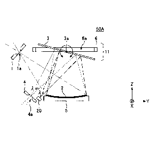
[0064] (Configuration of a Spectrometer 50A)
1100651 FIG. 16 is a conceptual view illustrating a configuration of a
spectrometer 50A
14
CA 03045981 2019-06-03
WO 2018/135223 PCT/JP2017/045752
according to the second embodiment of the present invention. The spectrometer
50A
illustrated in FIG. 16 is different from the spectrometer 10A according to the
first em-
bodiment (cf. FIG. 1) in terms of being further provided with a specific
wavelength
detecting device 20.
[0066] The specific wavelength detecting device 20 is an example of a
"specific wavelength
detecting unit" in the present invention. The specific wavelength detecting
device 20 is
provided near the focal point of output light (i.e., the position of the light
output part
4). The specific wavelength detecting device 20 is capable of detecting light
with
specific wavelength Xs and is placed near the light output part 4. The
specific
wavelength detecting device 20 detects light with specific wavelength Xs so as
to
enable the spectrometer 50A to detect whether the deflection angle range of
the
movable light reflection part 3 is sufficient for measuring a desired range of
wavelengths (Xm to kx) or whether the deflection angle range is constant.
[0067] For example, in a case of employing an InGaAs photodiode as a light
detecting
device, the range of wavelengths measured by the spectrometer 50A can be set
to 900
to 1700 nm or 900 to 2500 nm. In the above case, the specific wavelength Xs
may be
shorter than 900 nm, which is the minimum wavelength in the measuring range of
wavelengths, and may be longer than 1700 nm or 2500 nm, which is the maximum
wavelength in the measuring range of wavelengths. Specifically, in a case of
setting
the specific wavelength Xs to be equal to or shorter than around 1000 nm, the
above
configuration can be achieved with a lower cost because a Si photodiode can be
employed.
[0068] Note that dashed lines of FIG. 16 schematically indicate a light
path for light with the
minimum wavelength Xm in the measuring range of wavelengths. Furthermore,
dashed-dotted lines of FIG. 16 schematically indicate a light path for light
with the
specific wavelength Xs.
[0069] (Configuration of the Specific Wavelength Detecting Device 20)
[0070] The following description explains a specific configuration of the
specific
wavelength detecting device 20, with reference to FIGS. 17 and 18. FIG. 17 is
a
conceptual view illustrating a configuration (i.e., a first example) of a
specific
wavelength detecting device 20 according to the second embodiment of the
present
invention. For example, as illustrated in FIG. 17, the specific wavelength
detecting
device 20 is configured with a light detecting element 21 and a band-pass
filter 22. The
light detecting element 21 is an example of a "light detector" in the present
invention.
The light detecting element 21 detects light with specific wavelength Xs. As
the light
detecting element 21, a Si photodiode, and InGaAs photodiode, etc., may be
employed.
The band-pass filter 22 allows transmission of light with a particular range
of
wavelengths (including the specific wavelength Xs in the range). It is
preferable that, as
15
CA 03045981 2019-06-03
WO 2018/135223 PCT/JP2017/045752
the band-pass filter 22, a filter (e.g., a Fabry-Perot filter, etc.) with a
narrow passband
is employed.
[0071] FIG. 18 is a conceptual view illustrating a configuration (i.e., a
second example) of a
specific wavelength detecting device 20 according to the second embodiment of
the
present invention. As illustrated in FIG. 18, the specific wavelength
detecting device
20 may be further configured with a light interception member 23. The shape
and the
size of a light transmission part of the light interception member 23 may be
properly
chosen, based on requirements. Note that, instead of employing a band-pass
filter 22, a
light interception member 23, and a light detecting element 21, a light
detecting
element having functions as a bandpass filter and a light interception member
may be
employed for the specific wavelength detecting device 20. Furthermore, FIG. 27
is a
conceptual view illustrating another configuration of the spectrometer 50A
according
to the second embodiment of the present invention. Similarly to the
configuration il-
lustrated in FIG. 27, the specific wavelength detecting device 20 may be
integrally
formed on the light output part 4. For example, in a case where the light
output part 4
is formed out of a Si substrate and where the specific wavelength detecting
device 20
is a Si photodiode, the light output part 4 and the specific wavelength
detecting device
20 may be formed monolithically. Furthermore, as the band-pass filter 22 can
be
formed out of a Fabry-Perot filter, etc., by means of a semiconductor process
and the
light interception member 23 can be formed out of a metal thin film, etc., by
means of
a semiconductor process, the configuration of the specific wavelength
detecting device
20 illustrated in FIG. 18 can be integrally formed on the light output part 4.
Fur-
thermore, depending on the shape of the Si photodiode, a similar function may
be
obtained, even without forming the light interception member 23.
[0072] FIGS. 19 through 21 are drawings illustrating an example of an
output signal of the
specific wavelength detecting device 20 according to the second embodiment of
the
present invention. In FIGS. 19 through 21, examples of an output signal in a
case of
detecting light with specific wavelength Xs by means of the specific
wavelength
detecting device 20 are illustrated. In a case where resonance frequency of
the movable
light reflection part 3 is f, the driving cycle T is 1/f.
[0073] FIG. 19 is a drawing illustrating a situation where amplitude of
deflection angle of
the movable light reflection part 3 conforms to a measuring range of
wavelengths (i.e.,
km to Xx). In such a case as Xs = km, light with the specific wavelength Xs is
detected
at a position of the maximum deflection angle of the movable light reflection
part 3.
Therefore, the detection signal of the specific wavelength Xs is detected once
in a cycle
T.
[0074] FIG. 20 is a drawing illustrating a situation where amplitude of
deflection angle of
the movable light reflection part 3 is sufficient for a measuring range of
wavelengths
16
CA 03045981 2019-06-03
WO 2018/135223 PCT/JP2017/045752
(i.e., Xm to Xx). In this case, the detection signal of the specific
wavelength Xs is
detected twice in a cycle T.
[0075] FIG. 21 is a drawing illustrating a situation where amplitude of
deflection angle of
the movable light reflection part 3 is not sufficient for a measuring range of
wavelengths (i.e., Xm to Xx). In this case, amplitude of the detection signal
of the
specific wavelength Xs is decreased. When amplitude of deflection angle of the
movable light reflection part 3 is further decreased, the detection signal of
the specific
wavelength Xs is not output.
[0076] As a spectrometer is required to maintain a measuring range of
wavelengths (i.e.. Xm
to Xx) at all times, a situation of FIG. 19 or a situation of FIG. 20, in
which amplitude
of deflection angle of the movable light reflection part 3 is sufficient,
needs to be
maintained. Particularly, in the case of FIG. 20, it is possible to detect
that amplitude
of deflection angle of the movable light reflection part 3 is sufficient
without
depending on amplitude of the detection signal of the specific wavelength Xs,
by
detecting a time between two peaks, i.e., Td or Ts. Furthermore, by
controlling driving
of the movable light reflection part 3 such that Td or Ts is kept constant, it
is possible
to maintain a constant measuring range of wavelengths (i.e., Xm to Xx).
Furthermore,
by detecting light output through the light output part 4 in a range of Ts, it
is possible
to obtain a desired spectroscopic spectrum. Further, in a case where there is
possibility
that resonance frequency f of the movable light reflection part 3 fluctuates,
Td changes
with value off. Therefore, by measuring a cycle T (i.e., 1/0, it is possible
to control Td
to be constant in relation to resonance frequency f, so as to obtain a desired
spectrum.
[0077] Note that, as the range of T is a driving range for two-way motion
of the movable
light reflection part 3, two rounds of spectra are obtained practically. For
spectrum
data, a half of the obtained data or an average value of the obtained data may
be
utilized.
[0078] FIG. 22 is a drawing illustrating examples of a time waveform for
deflection angle of
the movable light reflection part 3 according to the second embodiment of the
present
invention. The solid line in FIG. 22 is indicative of a situation (i.e., the
situation of
FIG. 19) where deflection angle matches a measuring range of wavelengths and
where
light with a minimum wavelength Xm is output through the light output part 4
at the
time of a maximum value of deflection angle. The dashed line in FIG. 22 is
indicative
of a situation (i.e., the situation of FIG. 20) where deflection angle is
larger than the
measuring range of wavelengths. In this example, deflection angle exceeds an
angle
that corresponds to the minimum wavelength Xm, for time around a maximum value
of
deflection angle in the positive direction. Therefore, a specific wavelength
Xs is
detected at a timing of a deflection angle that corresponds to the minimum
wavelength
Xm. Accordingly, as illustrated in FIG. 20, two detection signals are
continuously
17
CA 03045981 2019-06-03
WO 2018/135223 PCT/JP2017/045752
detected in a cycle. The dashed-dotted line in FIG. 22 is indicative of a
situation (i.e.,
the situation of FIG. 21 or a situation where output of a specific wavelength
Xs is 0)
where deflection angle is not sufficient.
[0079] Note that a detection result of the specific wavelength detecting
device 20 is output
to the driving circuit 7 and is utilized for feedback-control of rotation
angle of the
movable light reflection part 3. In this case, for example, the driving
circuit 7 may
control a time interval (i.e., Td or Ts) of detection signals of the specific
wavelength Xs
to be constant, such that the movable light reflection part 3 is controlled to
have a
constant range of rotation angles.
[0080] (Variation Examples of a Configuration of a Spectrometer)
[0081] The following description explains variation examples of a
configuration of a spec-
trometer. Note that, in the following explanation of each of the variation
examples,
difference from the previously-explained spectrometers is explained.
Furthermore, in
each of the variation examples, constituent elements having the same function
as a
previously-explained constituent element are assigned the same reference sign
as the
previously-explained constituent element for omitting explanation.
Furthermore, the
operational mechanism, etc., of a spectrometer is the same as previously
explained, and
therefore the explanation is omitted in each variation example.
[0082] (First Variation Example)
[0083] FIG. 23 is a conceptual view illustrating a first variation example
of a configuration
of a spectrometer according to the second embodiment of the present invention.
A light
incidence part 1 and a movable light reflection part 3 of a spectrometer 50B
illustrated
in FIG. 23 are formed on a single substrate 6. Furthermore, a light output
part 4, a
concave diffraction grating 2, and a specific wavelength detecting device 20
of the
spectrometer 50B are formed on a single substrate 5. For example, in a case of
employing Si substrates for the substrates 5 and 6, the light incidence part 1
and the
light output part 4 may be integrally formed on the substrate 6 and the
substrate 5, re-
spectively, by means of a semiconductor process, a MEMS process, etc.
[0084] The specific wavelength detecting device 20 of the spectrometer 50B
may include a
light detecting element 21 and a band-pass filter 22 (cf. FIG. 17) and may
further
include a light interception member 23 (cf. FIG. 18). In the former case, the
light
detecting element 21 and the band-pass filter 22 can be monolithically formed
on the
substrate 5 because the light detecting element 21 and the band-pass filter 22
can be
formed out of a Fabry-Perot filter, etc., by means of a semiconductor process.
In the
latter case, the light interception member 23 can be also formed integrally
with the
light detecting element 21 and the band-pass filter 22 because the light
interception
member 23 can be formed out of a metal thin film, etc., by means of a
semiconductor
process.
Is
CA 03045981 2019-06-03
WO 2018/135223 PCT/JP2017/045752
[0085] In a case of the spectrometer 50B, which has the above-described
configuration, a
spectrometer can be smaller-scale because the specific wavelength detecting
device 20
can be integrally formed on the substrate 5. Furthermore, in a case of the
spectrometer
50B, the positional relation between the light output part 4 and the specific
wavelength
detecting device 20 can be controlled with a high degree of accuracy by
forming the
light output part 4 and the specific wavelength detecting device 20 by means
of a semi-
conductor process. Therefore, in a case of the spectrometer 50B, deflection
angle of the
movable light reflection part 3 can be detected with a high degree of
accuracy, so as to
stabilize a measuring range of wavelengths.
[0086] (Second Variation Example)
[0087] FIG. 24 is a conceptual view illustrating a second variation example
of a con-
figuration of a spectrometer according to the second embodiment of the present
invention. A spectrometer 50C illustrated in FIG. 24 is different from the
spectrometer
50B illustrated in FIG. 23 in terms of the point that a light output part 24
is formed at a
focal point of light with specific wavelength Xs and that a specific
wavelength
detecting device 20 is placed externally. The light output part 24 is an
example of a
"second light output unit" in the present invention. In a case of the
spectrometer 50C,
which has the above-described configuration, a process for the substrate 5 can
be
simplified because the specific wavelength detecting device 20 is not formed
on the
substrate 5. Furthermore, as the light output part 4 and the light output part
24 can be
formed on the substrate 5 simultaneously in a single process, the position
relation
between the light output part 4 and the light output part 24 can be controlled
with a
high degree of accuracy. Therefore, in a case of the spectrometer 50C,
deflection angle
of the movable light reflection part 3 can be accurately detected, so as to
stabilize a
measuring range of wavelengths.
[0088] (Third Variation Example)
[0089] FIG. 25 is a conceptual view illustrating a third variation example
of a configuration
of a spectrometer according to the second embodiment of the present invention.
A
spectrometer 50D illustrated in FIG. 25 is different from the spectrometer 50C
il-
lustrated in FIG. 24 in terms of the point that a light detecting element 21
and a band-
pass filter 22, which are constituent elements of a specific wavelength
detecting device
20, are placed separately. Specifically, the band-pass filter 22 is placed on
a substrate 5
so as to cover a light output part 24. Further, the light detecting element 21
is placed
externally. In a case of the spectrometer 50C, which has the above-described
con-
figuration, a spectrometer can be smaller-scale because only a light detecting
element
21 is placed externally, in comparison with a configuration in which a band-
pass filter
22 is externally placed as well.
1100901 (Fourth Variation Example)
19
CA 03045981 2019-06-03
WO 2018/135223 PCT/JP2017/045752
100911 FIG. 26 is a conceptual view illustrating a fourth variation example
of a con-
figuration of a spectrometer according to the second embodiment of the present
invention. A spectrometer 50E illustrated in FIG. 26 is different from the
spectrometer
50B illustrated in FIG. 23 in terms of the point that a specific wavelength
detecting
device 20 is arranged on the left (i.e., in the negative direction of the Y-
axis in FIG.
26) of the light output part 4 on the substrate 5. The positional change is
made in as-
sociation with setting the specific wavelength Xs to be longer than the
maximum
wavelength Xx in the measuring range of wavelengths. That is to say, the
specific
wavelength detecting device 20 is placed at a position where light with the
specific
wavelength Xs focuses when light with the maximum wavelength Xx passes the
light
output part 4.
1100921 Particularly, in a case where the maximum wavelength Xx in the
measuring range of
wavelengths is equal to or shorter than 2000 nm, there may be a configuration
in which
higher-order diffracted light with specific wavelength Xs' is detected at the
focal point
of light with the specific wavelength Xs. Although Xm, ?A, and Xs as explained
above
are first-order diffracted light, there is superimposition of second-order
diffracted light
at half wavelength for each position of the first-order diffracted light,
according to the
principle of diffraction. For example, in a case where the specific wavelength
Xs with
respect to first-order diffracted light is 2000 nm, there is second-order
diffracted light
with a wavelength of 1000 nm (i.e., Xs' = Xs/2) that focuses at the same
position of the
focal point of the first-order diffracted light. Therefore, as a less
expensive Si
photodiode can be employed in a case of detecting second-order diffracted
light with
wavelength Xs', cost-saving is possible.
1100931 Note that the specific wavelength detecting device 20 explained in
the second em-
bodiment may be applied to all of the spectrometers 10A through 101 explained
in the
first embodiment.
1100941 Furthermore, a spectrometer explained in each of the embodiments
may be
employed, together with a light source, to configure an analysis equipment.
For
example, in the analysis equipment, light of measurement is emitted by the
light source
towards a measurement object. Then, the light of measurement that is diffused
and
reflected by the measurement object is dispersed by a spectrometer. on a
wavelength
basis, so as to detect the light of measurement with each wavelength. In this
way, the
analysis equipment is capable of obtaining a spectroscopic spectrum of each
wavelength, which is characteristic depending on molecular structure of the
mea-
surement object. Furthermore, a spectrometer explained in each of the
embodiments
may be employed, together with a light source, to configure a wavelength-
variable
light source. An analysis equipment and a wavelength-variable light source
using a
spectrometer according to each of the embodiments as described above can be
85316696
achieved in a smaller scale and with a lower cost, as the spectrometer is
small-scale
and inexpensive.
[0095] FIG. 28 is a conceptual view illustrating a configuration of a
spectroscopic mea-
surement apparatus 70 by use of a spectrometer 10A according to the first
embodiment
of the present invention. The spectroscopic measurement apparatus 70
illustrated in
FIG. 28 is configured with the spectrometer 10A illustrated in FIG. 1, a light
detecting
device 30 placed outside of the light output part 4, and a light source 31. In
the spec-
troscopic measurement apparatus 70, light is emitted by the light source 31
towards a
measurement object 90, and then light reflected by the measurement object 90
is
incident from the light incidence part 1 to the spectrometer 10A. Light
diffracted by
the concave diffraction grating 2 is reflected by the movable light reflection
part 3 and
then, after being output through the light output part 4 in accordance with
tilt of the
movable light reflection part 3, is detected by the light detecting device 30.
In the
above way, the spectroscopic measurement apparatus 70 is capable of obtaining
an ab-
sorption spectroscopy spectrum of the measurement object 90. Note that the
detail of
the operational mechanism in the spectroscopic measurement apparatus 70 is the
same
as previously explained, and therefore the explanation is omitted here.
[0096] The above describes favorable embodiments of the present invention.
However, the
present invention is not limited to the embodiments, and various variations
and modi-
fications may be made without departing from the scope of the present
invention.
[0097] The present application is based on Japanese priority application
No. 2017-008806
filed on January 20, 2017, with the Japanese Patent Office, and Japanese
priority ap-
plication No. 2017-178919 filed on September 19, 2017, with the Japanese
Patent
Office.
Reference Signs List
[0098] 1 light incidence part (i.e., light incidence unit)
2 concave diffraction grating (i.e., diffraction grating)
3 movable light reflection part (i.e., reflection unit)
4 light output part (i.e., light output unit)
5 substrate (i.e., second substrate)
6 substrate (i.e., first substrate)
7 driving circuit (i.e., driving unit)
8 beam part
10A through 101 spectrometer
11 light reflection unit
14 resin layer
15 reflection member
Date Recue/Date Received 2020-10-30
21
CA 03045981 2019-06-03
WO 2018/135223
PCT/JP2017/045752
17 spacer (i.e., intervening member)
18 light detecting part (i.e., light detecting unit)
19 substrate (i.e., third substrate)
20 specific wavelength detecting device (i.e., specific wavelength detecting
unit)
21 light detecting element (i.e., light detector)
22 band-pass filter
23 light interception member
24 light output part (i.e., second light output unit)
50A through 50E spectrometer