Note: Descriptions are shown in the official language in which they were submitted.
CA 03046162 2019-06-05
WO 2018/109441 PCT/GB2017/053674
NON-VOLATILE MEMORY
The present invention relates to a non-volatile memory (NVM) cell and to a
method
of writing data to and reading data from a non-volatile memory cell.
The present invention aims to fill the gap between the high performance,
volatile,
expensive computer random access memory (RAM) and the low performance, low
cost,
non-volatile data storage devices such as hard disk drives (HDDs). Emerging
NVM
technologies attempting to fill this gap are referred to as storage class
memory (SCM).
In terms of improving the performance of data storage, the main candidate is
NAND-Flash, the dominant technology in solid state drives (SSDs), which is
currently too
expensive to replace HDDs and its low endurance, performance, and energy
efficiency
prevent its application as RAM. Improved HDD technology such as the Heat
Assisted
Magnetic Recording (HAMR) also suffers from low performance. Among non-
volatile
memory technologies under development the main contenders are spin-transfer
torque
RAM (STT-RAM, suffers from limited scalability, requires relatively high
current
densities to achieve switching between states), Ferroelectric RAM (FRAM, uses
destructive readout and suffers from lower endurance), Phase-change memory
(PCM,
suffers from low endurance, energy efficiency and relies on expensive, toxic
materials),
Resistive RAM (RRAM, uses destructive readout and the passive memory arrays
suffer
from the sneak path problem) and multicell devices based on these principles.
Existing NVM cells suffer from one or more of the following disadvantages:
they
require a transistor for reading and/or writing data, they require more than
two electrodes
for reading and writing data, they are not stackable and so cannot be formed
in three-
dimensional arrays, they have low packing density in two dimensions.
Summary of Invention
The present invention provides a non-volatile memory cell comprising: a
storage
layer comprised of a ferromagnetic material in which data is recordable as a
direction of
magnetisation; a piezomagnetic layer comprised of an antiperovskite
piezomagnetic
material selectively having a first type of effect on the storage layer and a
second type of
effect on the storage layer dependent upon the strain in the piezomagnetic
layer; a strain
inducing layer for inducing a strain in the piezomagnetic layer thereby to
switch from the
first type of effect to the second type of effect.
Therefore, the present invention makes use of the changing properties of
antiperovskite piezomagnetic materials with varying strain selectively to vary
the strength
of the interaction between the storage layer and the piezomagnetic layer. The
two types of
1
CA 03046162 2019-06-05
WO 2018/109441 PCT/GB2017/053674
effect allow writing to the memory cell. The magnetisation in the storage
layer affects a
magnetic state in the piezomagnetic layer. The magnetic state in the
piezomagnetic layer
affects the elastic properties of the piezomagnetic layer due to its strong
magneto-elastic
coupling. The piezomagnetic layer forms the top plate of a planar capacitor
and measuring
its capacity is used to read the magnetic state of the storage layer (the
magneto-capacitance
effect) using only two electrodes.
In an embodiment, the first type of effect is one where a net magnetisation of
the
piezomagnetic layer is strong enough to overcome the coercive field in the
storage layer
and for the magnetisation of the storage layer to align with the magnetisation
of the
piezomagnetic layer through dipolar coupling and the second type of effect is
one where
any magnetic field in the storage layer due to any magnetisation of the
piezomagnetic layer
is lower than the coercive field of the storage layer. Therefore, in the
second type of effect
the magnetisation of the storage layer does not change direction.
Therefore, in order to write information, voltage is applied to the
piezoelectric layer
which induces strain in the piezomagnetic layer to change its magnetisation.
The change
in magnetisation of the piezomagnetic layer is effective to change the
direction of
magnetisation of the storage layer due to dipolar coupling between the storage
layer and
the piezomagnetic layer. After the direction of magnetisation of the storage
layer has been
changed, the strain in the strain inducing (piezoelectric) layer is reduced to
a small value
(e.g. non-zero value) due to a small lattice mismatch between the
piezomagnetic and
strain-inducing layers or due to the ferroelectric polarisation of the strain-
inducing layer,
such that the magnetisation in the piezomagnetic layer reduces to a level such
that any
magnetic field in the storage layer is lower than the coercive field of the
storage layer.
Thereby the direction of magnetisation in the storage layer is unchanged once
the strain is
removed from the piezomagnetic layer (once the voltage is removed from the
piezoelectric
layer).
The advantage of this arrangement is that the same electrodes as used for
writing to
the storage layer can be used for reading the storage layer.
In an embodiment, the non-volatile memory cell comprises a non-magnetic layer
between the storage layer and the piezomagnetic layer for preventing an
exchange bias
between the storage layer and the piezomagnetic layer. If an exchange bias
existed
between the storage layer and the piezomagnetic layer, when the strain applied
to the
piezomagnetic layer in order to write to the storage layer is removed, the
direction of
magnetisation in the storage layer would also be affected. Thereby including a
non-
2
CA 03046162 2019-06-05
WO 2018/109441 PCT/GB2017/053674
magnetic layer between the storage layer and the piezomagnetic layer allows
voltage to be
removed from the NVM cell without losing the data stored in the storage layer.
In an embodiment, the antiperovskite piezomagnetic material has a Neel
temperature (TN) greater than 350K at a strain of +/- 30%, preferably +/- 10%,
most
preferably +/- 1%. This means that the antiperovskite piezomagnetic material
will
maintain its piezomagnetic properties at typical operating temperatures of the
non-volatile
memory cell and will not require, for example, any special cooling
arrangements to ensure
that the material does not rise above the Neel temperature and thereby become
paramagnetic.
In an embodiment, the antiperovskite piezomagnetic material is a Mn3SnN based
material (e.g. Mn3_xA,Sni-yByNi_z, where A and B are one or more elements
selected from
the list including: Ag, Al, Au, Co, Cu, Fe, Ga, Ge, In, Ir, Ni, Pd, Pt, Rh,
Sb, Si, Sn, Zn).
Mn3SnN is a material which has been found to have a Neel temperature of about
475 K as
well as a large change in the induced magnetisation for a small change in
strain and can
thereby provide a high degree of reliability.
In an embodiment, the first type of effect is one in which the piezomagnetic
layer is
in the paramagnetic state and no exchange bias interaction between the storage
layer and
the piezomagnetic layer is present thereby allowing the direction of
magnetisation of the
storage layer to be changed by an external magnetic field and the second type
of effect is
an exchange bias interaction in which the piezomagnetic material is in the
antiferromagnetic state so the direction of magnetisation of the storage layer
is pinned by
the piezomagnetic layer. An external magnetic field may be a switchable field
applied
globally to the whole array or locally to each bit or a constant perpendicular
field driving a
precessional magnetisation switching. In this embodiment, the newly discovered
property
of antiperovskite piezomagnetic materials that they exhibit a change in Neel
temperature
with strain is applied to the non-volatile memory cell. This allows, when the
antiperovskite piezomagnetic material is paramagnetic, for the direction of
magnetisation
of the storage layer to be varied. The strain applied to the piezomagnetic
material is then
released returning the antiperovskite piezomagnetic material to an
antiferromagnetic state
when it pins the direction of magnetisation of the storage layer by exchange
bias
interaction. Thereby the direction of magnetisation in the storage layer is
maintained even
when no voltage is applied to the memory cell. Thus, such a memory cell is non-
volatile,
highly resilient to thermal fluctuations or external magnetic fields, and not
power hungry.
In an embodiment, the piezomagnetic material has a Neel temperature which
varies
with strain and wherein the Neel temperature passes 293 K when the strain is
varied from +
3
CA 03046162 2019-06-05
WO 2018/109441 PCT/GB2017/053674
30% to -30%, preferably + 10% to -10%, most preferably + 1% to -1%. This means
that
the device can be operated at typical ambient temperatures and no heating or
cooling (such
as in HAMR) is necessary in order for the NVM cell to operate correctly.
In an embodiment, the antiperovskite piezomagnetic material is Mn3GaN or
Mn3NiN based e.g. Mn3_,AxGai-yByN:_z or Mn3-xAxNi -yByN -z, where A and B are
one or
more elements selected from the list including: Ag, Al, Au, Co, Cu, Fe, Ga,
Ge, In, Ir, Ni,
Pd, Pt, Rh, Sb, Si, Sn, Zn. A number of these materials have been found to
exhibit a
change in Neel temperature which varies with strain wherein the Neel
temperature passes
293 K when the strain is varied from + 1% to -1% and also exhibit a large
change in Neel
temperature in that strain range, thereby allowing easier control of the
writing to the
storage layer.
In an embodiment, the non-volatile memory cell comprises at least one
additional
electrode positioned adjacent the storage layer to induce a global or a local
time dependent
magnetic field for changing the direction of magnetisation of the storage
layer. In an
embodiment, the additional layer has constant magnetisation perpendicular to
the
magnetisation of the storage layer to induce precessional switching of the
magnetisation of
the storage layer when it becomes unpinned for one half of its precession
period. This
further mechanism is advantageous in the embodiment where the piezomagnetic
material is
made paramagnetic in a write procedure in order to unpin the storage layer. A
single
source of the applied magnetic field can be used to write data to multiple
memory cells.
In a preferred embodiment, the strain inducing layer is a piezoelectric layer.
This
allows fast switching between different strain rates and excellent durability.
In an embodiment, the strain inducing layer is a perovskite material. This is
advantageous as it is then possible to reduce any lattice mismatch between the
strain
inducing layer and the piezomagnetic layer. With a lower lattice mismatch both
tensile
and compressive strain can be induced in the piezomagnetic layer by the strain
inducing
layer and also any remaining strain in the piezomagnetic layer when the strain
inducing
layer is not activated (i.e. due to lattice mismatch) is reduced. This is
advantageous
because it improves the mechanical stability and durability of the memory
cell.
In an embodiment, a lattice mismatch between the storage layer and the
piezomagnetic layer and/or between the piezomagnetic layer and the strain
inducing layer
is less than 1%. This increases the durability of the device and in the case
of low mismatch
between the piezomagnetic layer and the inducing layer allows for both tensile
and
compressive strains to be induced in the piezomagnetic layer and thereby
enables the write
operations in the first type of embodiment. In the case that the non-volatile
memory cell is
4
CA 03046162 2019-06-05
WO 2018/109441 PCT/GB2017/053674
part of a two or three-dimensional array of memory cells, small lattice
mismatch enables
large arrays to be built which would otherwise have unacceptable levels of
strain in them.
In an embodiment, the storage layer is a perovskite layer. This is
advantageous as
the lattice mismatch between adjacent perovskite and antiperovskite layers
allows low
lattice mismatch between the layers with the accompanying advantages mentioned
above.
In an embodiment, the non-volatile memory cell further comprises: a first
electrode
connected to the storage layer on a side opposite the piezomagnetic layer; and
a second
electrode connected to the strain inducing layer on a side opposite the
piezomagnetic layer.
The non-volatile memory can then be read and written to with only those two
electrodes
and without the need for a transistor at each cell of the array. Thus, the NVM
cell is easily
addressable. In a two-dimensional array, individual memory cells can be
addressed with
first and second electrodes shared with other cells of the array.
In an embodiment, there is provided a two- or three- dimensional array of
memory
cells comprising a plurality of non-volatile memory cells of the present
invention. The
memory cells of the present invention are ideally suited to being incorporated
into a two or
three-dimensional array because, particularly if built with low lattice
mismatch between
the layers, stresses are not built up as more memory cells are formed adjacent
one another,
both laterally and vertically. The size of each memory cell is small and the
need for only
two electrodes to perform both the read and write functions means that a high
density
memory can be achieved.
In an embodiment, there is provided a method of writing data to and reading
data
from a non-volatile memory cell comprising a storage layer and an
antiperovskite
piezomagnetic layer, the method comprising the steps of: inducing a
polarisation in a first
or second direction in the storage layer thereby to write data to the memory
cell,
polarisation of the storage layer in the first direction inducing a first
magnetic state in the
antiperovskite piezomagnetic layer and polarisation of the storage layer in
the second
direction inducing a second magnetic state in the antiperovskite piezomagnetic
layer, and
measuring a magneto-capacitance of the memory cell, the magneto-capacitance of
the
antiperovskite piezomagnetic layer being different in the first magnetic state
than in the
second magnetic state, thereby to read the data stored in the storage layer.
Thus, the information stored in the storage layer can be read using only two
electrodes and without the need for a transistor and without overwriting the
data stored in
the memory. This is not achievable without the antiperovskite piezomagnetic
layer as the
capacity of a general ferroelectric capacitor is symmetric about the
orientation of its
electric polarisation. That is, the magneto-capacitance of the memory bit when
measured
CA 03046162 2019-06-05
WO 2018/109441 PCT/GB2017/053674
in a fully compensated antiferromagnetic state or paramagnetic state of the
antiperovskite
piezomagnetic layer is the same irrespective of the direction of the
ferroelectric
polarisation. Conversely, for the canted antiferromagnetic state of the
antiperovskite
piezomagnetic layer, the magneto-capacitance varies with the orientation of
the
ferroelectric polarisation which affects the size of the magnetisation in the
piezomagnetic
layer. This is due to the frustrated magnetism of the antiperovskite
piezomagnetic material
underpinning the so called magneto-elastic coupling.
In an embodiment, the measuring comprises applying an alternating voltage
across
the storage layer and antiperovskite layer and determining a reactance and
thereby the
magneto-capacitance of the memory cell. In an embodiment, the measuring
comprises
determining a shift in resonance frequency of the memory cell.
In an embodiment, the storage layer is comprised of a ferromagnetic material
and
the polarisation is a magnetic polarisation i.e. a magnetisation.
In an embodiment, the inducing is performed by inducing a magnetisation in the
antiperovskite piezomagnetic layer strong enough for the magnetic polarisation
of the
storage layer to align with the magnetisation of the antiperovskite
piezomagnetic layer
through dipolar coupling. Thus, the antiperovskite piezomagnetic material has
two
functions, both allowing the memory cell to be read and also being used in the
write
operation to induce the polarisation in the storage layer. This means that
only two
electrodes are needed to perform both the read and write functions and this
without
needing a transistor which uses power and uses up space.
In an embodiment, the non-volatile memory further comprises a strain inducing
layer and inducing a magnetisation in the antiperovskite piezomagnetic layer
is achieved
by inducing a strain in the antiperovskite piezomagnetic layer using the
strain inducing
layer. Thus, by applying a potential difference across the strain inducing
layer (which can
be a piezoelectric material), a strain can be induced in the antiperovskite
piezomagnetic
layer. A strain in the antiperovskite piezomagnetic layer results in the
generation of a
magnetic spin polarisation in the antiperovskite piezomagnetic layer. The
magnetic spin
polarisation in the antiperovskite piezomagnetic layer thereby induces the
magnetisation in
the storage layer, for example by dipolar coupling.
In an embodiment, the inducing comprises inducing a magnetisation in the
storage
layer using a magnetisation electrode. Such a magnetisation electrode can be
used to
induce polarisation in the first or second direction in the storage layer of
multiple non-
volatile memory cells.
6
CA 03046162 2019-06-05
WO 2018/109441 PCT/GB2017/053674
In an embodiment, the inducing further comprises inducing a strain in the
antiperovskite piezomagnetic layer thereby to turn the antiperovskite
piezomagnetic layer
paramagnetic. In this embodiment, the antiperovskite piezomagnetic layer is
used as a
switch to allow writing on the storage layer or not to allow writing on the
storage layer.
Thereby in combination with the externally applied magnetic field, a system of
reading and
writing data to and from the non-volatile memory cell can be achieved.
In an embodiment, the non-volatile memory cell further comprises a strain
inducing
layer and the inducing strain is accomplished by the strain inducing layer.
Thus, by
applying a potential difference across the strain inducing layer (which can be
a
piezoelectric material), a strain can be induced in the antiperovskite
piezomagnetic layer.
This can be used to turn the antiperovskite piezomagnetic layer from an
antiferromagnetic
material into a paramagnetic material. This switch has fast response times and
good
longevity and can be used to pin and not to pin the polarisation in the
storage layer.
In an embodiment, the storage layer is comprised of a ferroelectric material
and the
polarisation is an electric polarisation. In this embodiment, the non-volatile
memory cell
comprises a first electrode connected to the antiperovskite piezomagnetic
layer on a side
opposite the storage layer and a second electrode connected to the storage
layer on a side
opposite the antiperovskite piezomagnetic layer, and the inducing comprises
applying a
potential difference across the first and second electrodes, and the measuring
comprises
measuring the magneto-capacitance between the first and second electrodes.
Such a device
is extremely simple and compact and may be operated inside a transistor-less
array.
Embodiments of the invention will now be described by way of example only with
reference to and as illustrated in the following drawings:
Figure 1 is a schematic illustration of the lattice and magnetic structure of
an
antiperovskite piezomagnetic material;
Figure 2 is a graph of strain along the x-axis vs induced net magnetisation
along the
y axis for a selection of different antiperovskite piezomagnetic materials;
Figure 3 is a graph of strain along the x-axis vs (Neel temperature ¨ Neel
temperature at zero strain) in Kelvin along the y axis for a selection of
different
antiperovskite piezomagnetic materials;
Figure 4 is a graph of experimentally determined results for Mn3NiN ¨ Neel
temperature and saturation magnetisation on the y axis as a function of the c
axis strain on
the x axis with saturation magnetisation taken from M-H loops at 100K;
7
CA 03046162 2019-06-05
WO 2018/109441 PCT/GB2017/053674
Figure 5 is a graph of magneto-capacitance effect of
Mn3GaN/Bao 75Sr025TiO3/SrRu03 heterostructure on (LaA103)03(Sr2TaA106)0 7
substrate at
room temperature;
Figure 6 is a cross sectional schematic diagram of a non-volatile magnetic
memory
cell according to a first embodiment;
Figure 7 is a cross sectional schematic diagram of a non-volatile magnetic
memory
cell according to a second embodiment;
Figure 8 is a cross sectional schematic diagram of a non-volatile electric
memory
cell according to a third embodiment;
Figure 9 is a perspective schematic view of a two-dimensional magnetic memory
array according to an embodiment;
Figure 10 is an explanation of writing to a two-dimensional memory array of
the
first embodiment (and is also applicable to a two-dimensional memory array of
the third
embodiment);
Figure 11 is an explanation of writing a two-dimensional array of the second
embodiment;
Figure 12 is an explanation of reading of a two-dimensional memory array of
all
three embodiments; and
Figure 13 is a perspective schematic view of a three-dimensional magnetic
memory
array according to an embodiment.
The present invention makes use of the properties of Mn-based antiperovskites.
These materials are known to exhibit the piezomagnetic effect. The
piezomagnetic effect
is a change in magnetisation due to the application of a stress which is
manifested in the
canted antiferromagnetic state of the Mn-based antiperovskites.
Figure la illustrates the structure of a Mn-based antiperovskite in the
unstrained
state where there is no net magnetisation. Figure lb illustrates the case
where a tensile
strain is applied and there is an induced net magnetisation anti-parallel to
the [110]
direction, and Figure 1 c illustrates the case where a compressive strain is
applied which
induces a net magnetisation parallel to the [110] direction. As is
illustrated, on application
of a tensile strain or a compressive strain a net magnetic spin polarisation
(i.e.
magnetisation) is induced. The direction of magnetic spin polarisation is
opposite for
tensile and compressive strains.
Figure 2 is a graph along the x axis of percentage biaxial lattice strain and
along the
y axis of induced magnetisation. In Figure 2 the variation in induced
magnetisation is
8
CA 03046162 2019-06-05
WO 2018/109441 PCT/GB2017/053674
plotted for four different types of Mn-based antiperovskite material. As can
be seen, the
largest variation in magnetic field with strain occurs for Mn3SnN, with the
next most
sensitive material being Mn3NiN followed by Mn3InN and then Mn3GaN. Also
illustrated
is the Neel temperature at zero percent strain experimentally observed for
bulk form of
those materials. Above the Neel temperature, the materials become paramagnetic
rather
than antiferromagnetic and so the effect of change in magnetic spin
polarisation with
induced strain is not observed. The results in Figure 2 are the results of
simulations which
have been confirmed experimentally for Mn3NiN (see figure 4 which shows Neel
temperature and saturation magnetisation on the y axis as a function of the c
axis strain on
the x axis with saturation magnetisation taken from M-H loops at 100K).
The present inventors have discovered that the Neel temperature of Mn-based
antiperovskites changes strongly with induced strain. The sensitivity of the
Neel
temperature to induced strain is illustrated in Figure 3 where strain is
plotted along the x
axis and the deviation of the Neel temperature from its value at zero strain
in Kelvin along
the y axis for three different Mn-based antiperovskites. The results shown in
Figure 3 are
based on theoretical calculations which are known to overestimate the Neel
temperature
(using the KKR-DLM mean field approximation (quantum mechanical code developed
mainly by Professor J B Staunton at the University of Warwick)). Although the
values of
temperature in Kelvin are not representative of what is observed
experimentally, the
variations in Neel temperature are indicative of what is observed
experimentally. As can be
seen, both Mn3NiN and Mn3GaN exhibit a Neel temperature at around ambient
temperature (at zero percent strain the Neel temperatures are 240K (as seen in
Figure 4)
and 300K respectively, as determined experimentally). A change in strain in
the Mn-
based antiperovskite can be used to change the properties of the Mn-based
antiperovskite
from being piezomagnetic (below the Neel temperature) to being paramagnetic
(above the
Neel temperature). The results for the dependence of Neel temperature and
induced
magnetisation on strain in Mn3NiN have been confirmed experimentally (Figure
4).
Figure 5 shows the measured magneto-capacitance effect of
Mn3GaN/Bao 75Sr0 25TiO3/SrRu03 heterostructure on (LaA103)0 3(Sr2TaA106)0 7
substrate at
room temperature. The magneto-capacitance effect of more than 1400% under a
magnetic
field of 7T was obtained by applying a 1.5V DC bias between the bottom
electrode
(SrRu03) and a top electrode of Au. The change in the capacitance of Bao 75Sro
25TiO3
results from the interfacial strain induced by the (inverse) piezomagnetic
effect of the
Mn3GaN layer under the magnetic field. It is noted that the magneto-
capacitance effect is
9
CA 03046162 2019-06-05
WO 2018/109441 PCT/GB2017/053674
much less at a OV DC bias compared to the magneto-capacitance effect at 1.5V
DC bias.
The large magneto-capacitance underpins the reading mechanism.
The present inventors have developed NVM cells on the basis of the
understanding
illustrated in Figures 1-5 of the properties of Mn-based antiperovskites.
In the first and second embodiments, a non-volatile memory cell utilises the
properties of Mn-based antiperovskite piezomagnetic material illustrated in
Figures 2-5.
Figures 6 and 7 are cross-sectional schematic diagrams of non-volatile
magnetic memory
cells according to the first and second embodiments. The NVM cells comprise a
storage
layer 10 in which data is recordable. The storage layer 10 may be comprised of
a
ferromagnetic material. In this way, the data is recordable as a direction of
magnetisation.
A piezomagnetic layer 20 is also provided. The piezomagnetic layer 20 is
comprised of an antiperovskite piezomagnetic material, preferably Mn-based
antiperovskite piezomagnetic material. Depending upon the strain in the
piezomagnetic
layer 20, the piezomagnetic layer 20 selectively has a first type of effect on
the storage
layer 10 (for example when under a compressive or tensile strain) and a second
type of
effect on the storage layer 10 (for example under low or no tensile or
compressive strain).
A strain inducing layer 30 is provided for inducing a strain in the
piezomagnetic
layer 20 thereby to switch from the first type of effect to the second type of
effect.
A first electrode 50 is provided on a side of the storage layer 10 opposite to
the
piezomagnetic layer 20. A second electrode 60 is provided on a side of the
strain inducing
layer 30 opposite to the piezomagnetic layer 20. The layers 20, 30, and 60
form a planar
capacitor which exhibits the magneto-capacitance effect used to read out the
stored
information non-destructively by electrical means only (as described below).
By applying a voltage across the first and second electrodes 50, 60 a strain
may be
induced in the strain inducing layer 30. The strain induced by the potential
difference
across the first and second electrodes 50, 60 in the strain inducing layer 30
is transferred to
the piezomagnetic layer 20. As illustrated in Figures 2-5, inducing a strain
in the
piezomagnetic layer 20 changes the property of the piezomagnetic layer 20 in
terms of its
magnetisation and/or in terms of its Neel temperature. The change in property
of the
piezomagnetic layer 20 has an effect (e.g. the first type of effect) on the
storage layer 10
which is a different effect (e.g. the second type of effect) dependent upon
the strain in the
piezomagnetic layer 20.
In an embodiment, the piezomagnetic layer 20 is grown with the (001)
orientation
aligned perpendicular to the plane of the strain inducing layer 30 and the
storage layer 10.
This ensures good epitaxial growth, formation of the magnetic structure shown
in Figure 1,
CA 03046162 2019-06-05
WO 2018/109441 PCT/GB2017/053674
good mechanical stability, small lattice mismatch with the ferroelectric layer
30, and the
maximum change in property (magnetisation, first embodiment or Neel
temperature,
second embodiment) for a given in-plane strain.
The strain inducing layer 30 may be a piezoelectric material, for example a
ferroelectric material. In an embodiment, the strain inducing layer 30 has a
perovskite or
antiperovskite structure. For example, the strain inducing layer may be a
(Ba/Sr)TiO3
material. Having a perovskite structure may be advantageous because a well-
defined
interface and strong elastic coupling between the strain inducing layer 30 and
piezomagnetic layer 20 is thereby achievable. A clean crystalline interface
results in long
life of the non-volatile memory cell and a large transfer of the strain
induced in the strain
inducing layer 30 being transferred to the piezomagnetic layer 20.
Particularly in the case
of the first embodiment, a low lattice mismatch between the strain inducing
layer 30 and
piezomagnetic layer 20 is desirable. This is because when no potential
difference is
applied between the first and second electrodes 50, 60, it is desirable that
very little or no
strain exists in the piezomagnetic layer 20. When no potential difference is
applied, there is
zero magnetisation (or a small magnetisation induced by the spontaneous
electric
polarisation of the adjacent ferroelectric strain-inducing layer or residual
strain resulted
from lattice mismatch between the strain inducing layer 30 and piezomagnetic
layer 20) of
the piezomagnetic layer 20 and it is desirable to have as low a magnetisation
in the
piezomagnetic layer 20 as possible in the first embodiment when no potential
difference is
applied between the first and second electrodes 50, 60. Any mismatch between
the strain
inducing layer 30 and the piezomagnetic layer 20 may result in a strain in the
piezomagnetic layer 20 when zero potential difference is applied between the
first and
second electrodes 50, 60. As long as any magnetisation in the piezomagnetic
layer 20 at
zero potential difference is present between the first and second electrodes
50, 60 results in
a magnetic field in the storage layer 10 which is lower than the coercive
field of the storage
layer 10, that is acceptable.
The lattice constant of the strain inducing layer 30 and piezomagnetic layer
20 (and
between other layers) can be adjusted by changing the growth conditions and
composition
(as described below). In this way, the lattice mismatch between the various
layers can be
adjusted. Desirably the lattice mismatch between the storage layer 10 and the
piezomagnetic layer 20 and/or between the piezomagnetic layer 20 and the
strain inducing
layer 30 and/or between the first or second electrode 50/60 and its adjacent
layer is less
than 1%, more desirably less than 0.5%. This not only results in a long
lasting device and
other desirable properties as described elsewhere, but also means that it is
possible to
11
CA 03046162 2019-06-05
WO 2018/109441 PCT/GB2017/053674
develop a two- or even three- dimensional array of memory cells extending
laterally and
vertically which has a high degree of robustness.
The operation of the first embodiment of the present invention will now be
described in detail with reference to Figure 6. The embodiment of Figure 6
uses the
principle illustrated in Figure 2. That is, in order to write data to the
storage layer 10, a
potential difference is applied between the first and second electrodes 50, 60
in a certain
direction in order to contract or expand the strain inducing layer 30 and
thereby to apply a
compressive or tensile strain in the piezomagnetic layer 20. As a strain is
induced in the
piezomagnetic layer 20, a magnetisation will develop in the piezomagnetic
layer 20 in a
direction according to whether the strain is tensile or compressive. Through
dipolar
coupling between the piezomagnetic layer 20 and the storage layer 10, the
spontaneous
magnetisation of the storage layer 10 will be switched according to the
direction of
magnetisation of the piezomagnetic layer 20 in the first type of effect. In
this way, the
direction of magnetisation in the storage layer 10 can be changed by applying
a positive or
negative potential difference between the first and second electrodes 50, 60.
When the potential difference between the first and second electrodes 50, 60
is
removed, the strain inducing layer 30 returns to its original shape and the
strain in the
piezomagnetic layer 20 also returns to its original level (close to zero,
particularly if there
is low lattice mismatch between the piezomagnetic layer 20 and the strain
inducing layer
30). As a result, no magnetisation remains in the piezomagnetic layer once the
potential
difference between the first and second electrodes 50, 60 has been removed.
With negligible magnetisation in the piezomagnetic layer 20, and assuming that
there is no exchange bias effect between the piezomagnetic layer 20 and the
storage layer
10, the magnetisation of the storage layer 10 remains fixed by the magnetic
anisotropy
(coercive field) of the ferromagnetic storage layer (assuming no external
magnetic field)
and this is the second type of effect.
In an embodiment, in order to avoid exchange bias between the piezomagnetic
layer 20 and the storage layer 10, a (metallic) non-magnetic layer 15 may be
provided
between the storage layer 10 and the piezomagnetic layer 20. The non-magnetic
layer 15
may be relatively thin (of the order of a nanometre). For such a thin layer,
the lattice
constant of the material will match that of the adjacent layers (the
piezomagnetic layer 20
and the storage layer 10) such that no strain will be induced by the presence
of the non-
magnetic layer 15. The non-magnetic layer 15 prevents exchange bias between
the storage
layer 10 and the piezomagnetic layer 20. The prevention of exchange bias
between those
12
CA 03046162 2019-06-05
WO 2018/109441 PCT/GB2017/053674
two layers means that when the magnetisation in the piezomagnetic layer 20 is
removed,
any magnetisation in the storage layer 10 is unaffected.
Even if a small magnetisation remains in the piezomagnetic layer 20 after the
removal of the potential difference between the first and second electrodes
50, 60, so long
as any magnetic field acting on the storage layer 10 resulting from the
magnetisation of
layer 20 is lower than the coercive field of the storage layer 10, no change
in the
magnetisation of the storage layer 10 will occur. Therefore, the first
embodiment makes
use of magnetic anisotropy (combination of magneto-crystalline and shape
anisotropy) of
the ferromagnetic material of the storage layer 10. The lateral dimensions of
each memory
bit are smaller than typical magnetic domain sizes so the storage layer 10 is
assumed to be
in a single domain state where the coercive fields are determined by the
magnetic
anisotropy.
In order to change the data (direction of magnetisation) stored in the storage
layer
10, a potential difference opposite in direction to that previously applied is
applied between
the first and second electrodes 50, 60. This induces the opposite of a tensile
or
compressive strain in the strain inducing layer 30 and thereby in the
piezomagnetic layer
20 and so a magnetisation opposite in direction develops. Thereby, via the
dipolar
coupling, the direction of magnetisation in the storage layer 10 is changed.
In the first embodiment, the preferred antiperovskite piezomagnetic material
is
Mn3SnN or Mn3SnN based as this material according to Figure 2 exhibits the
greatest
change induced magnetic field with strain. The material can be optimised to
have a
desirable lattice parameter and piezomagnetic properties by changing its
chemical
composition, e.g., Mn3,A,Sni_yByNi_, where A and B are one or more elements
selected
from the list including: Ag, Al, Au, Co, Cu, Fe, Ga, Ge, In, Ir, Ni, Pd, Pt,
Rh, Sb, Si, Sn,
Zn. It could also be derived from other antiperovskite than Mn3SnN. In
general, it can be
any material with piezomagnetism at room temperature and good lattice match
with the
other layers.
In an embodiment, the piezomagnetic layer 20 is in contact with a surface of
the
strain inducing layer 30. In an embodiment, the non-magnetic layer 15 is in
contact with
the piezomagnetic layer 20. In an embodiment, the storage layer 10 is in
contact with the
non-magnetic layer 15. In an embodiment, the first electrode 50 is in contact
with the
storage layer 10. In an embodiment, the second electrode 60 is in contact with
the strain
inducing layer 30.
In an embodiment, the storage layer 10 is a perovskite or antiperovskite
material,
for example Co3FeN. The strain inducing layer 30 may be formed on an electrode
which
13
CA 03046162 2019-06-05
WO 2018/109441 PCT/GB2017/053674
itself is formed on a substrate, for example a substrate of MgO, SrTiO3,
Nb:SrTiO3 or Si.
In an embodiment, the substrate has lattice parameters which match those the
electrode and
strain inducing layer 30. In an embodiment, the substrate (for example
Nb:SrTiO3 or doped
Si) on which the layers are grown can be used as the electrode and a separate
electrode is
not needed.
The first electrode 50 can be made of a metal or a conducting perovskite such
as
Nb:SrTiO3 or SrRu03. The second electrode 60 may be made of Nb:SrTiO3 or
SrRu03.
In order to read the data stored in the storage layer 10, use is made of the
magneto-
capacitance effect. A further property of antiperovskite piezomagnetic
materials is that
their stiffness changes as a result of the magnetic field present in them due
to the magneto-
elastic coupling. The presence of magnetisation in the storage layer 10
results in a
magnetic field in the piezomagnetic layer 20 even at zero strain. The magnetic
field in the
piezomagnetic layer 20 results in a change in the elasticity of the
piezomagnetic layer 20
compared to when no magnetic field is present in the piezomagnetic layer 20.
The change
in elasticity in the piezomagnetic layer 20 can be measured as a change in the
magneto-,
capacitance of the capacitor formed by layers 20, 30, and 60. The change in
magneto-
capacitance is asymmetric, meaning that the measured capacity is different for
the two
opposite alignments of magnetisation in the storage layer 10. Thus, by
measuring the
magneto-capacitance of the capacitor formed by layers 20, 30, and 60 it is
possible to
determine the direction of magnetisation in the storage layer 10. Thereby by
measuring the
magneto-capacitance between the first and second electrodes 50, 60 the
direction of the
magnetisation in the storage layer 10 can be determined.
One way of measuring the magneto-capacitance between the first and second
electrodes 50, 60 comprises applying an alternating voltage between the first
and second
electrodes 50, 60 and measuring the response (reactance). This is explained
further below
with reference to Figure 10.
Thereby with only two electrodes it is possible to both write to the storage
layer 10
and read from the storage layer 10 without the need for a transistor and
without the need
for a third or more electrodes. This is desirable as designs of two or three-
dimensional
memories comprising plural non-volatile memory cells of the present invention
are
possible which are particularly compact and simple in design.
A second embodiment will now be described with reference to Figure 7. The
second embodiment is the same as the first embodiment except as described
below.
The second embodiment relies on the behaviour of the piezomagnetic layer 20 as
illustrated in Figures 3-5. That is, the property of the piezomagnetic layer
20 is switched
14
CA 03046162 2019-06-05
WO 2018/109441 PCT/GB2017/053674
from antiferromagnetic behaviour (second type of effect) to paramagnetic
behaviour (first
type of effect) by inducing a strain in it (and thereby changing the Neel
temperature to
below the temperature experienced by the piezomagnetic layer 20). In the
second
embodiment, the non-magnetic layer 15 of the first embodiment is omitted. As a
result, an
exchange bias exists between the storage layer 10 and the piezomagnetic layer
20 when the
piezomagnetic layer is antiferromagnetic (e.g. when no potential difference is
applied
between the first and second electrodes 50, 60).
When a potential difference is applied between the first and second electrodes
50,
60, the strain induced by the strain inducing layer 30 in the piezomagnetic
layer 20 is
effective to lower the Neel temperature of the piezomagnetic layer 20 such
that the
antiperovskite piezomagnetic layer 20 becomes paramagnetic. When the
piezomagnetic
layer 20 is paramagnetic, no exchange bias exists between the piezomagnetic
layer 20 and
the storage layer 10. However, when the piezomagnetic layer 20 is
antiferromagnetic (e.g.
after the potential difference is turned off), an exchange bias does exist
between the
piezomagnetic layer 20 and the storage layer 10. When an exchange bias exists
between
the piezomagnetic layer 20 and the storage layer 10, the direction of
magnetisation of the
storage layer 10 is fixed, even if a magnetic field greater in strength than
the coercive field
is present. Layer 20 can fix the magnetisation of layer 10 to at least two
different directions
depending on the magnetic state of layer 10 present when layer 20 turns
antiferromagnetic.
The second embodiment thereby applies a potential difference between the first
and
second layers 50, 60 to induce a strain in the piezomagnetic layer 20 (through
the strain
inducing layer 30) to change the properties of the piezomagnetic layer 20
between canted
antiferromagnetic and paramagnetic. Once the piezomagnetic layer 20 is
paramagnetic, it
is possible to change the direction of magnetisation in the storage layer 10.
This can be
achieved, for example using an external magnetic field. For this purpose, at
least one
additional electrode 70 inducing a magnetic field or a perpendicularly
magnetised layer 70
can be provided, for example. Individual additional electrodes 70 can act
globally over two
or more memory cells, or locally to a single memory cell. Alternatively, an
additional layer
with constant magnetisation perpendicular to the magnetisation of the storage
layer 10 is
included to induce precessional switching of the magnetisation of the storage
layer 10
when it becomes unpinned for one half of its precession period. This further
mechanism is
advantageous in the embodiment where the piezomagnetic material 20 is made
paramagnetic in a write procedure in order to unpin the storage layer 10. By
inducing a
magnetic field in the storage layer 10 using the electrode 70, the direction
of magnetisation
of the storage layer 10 can be changed. After the direction of magnetisation
in the storage
CA 03046162 2019-06-05
WO 2018/109441 PCT/GB2017/053674
layer 10 has been changed, thereby to write data to the storage layer 10, the
potential
difference applied across the first and second electrodes 50, 60 is removed.
Thereby the
Neel temperature of the piezomagnetic layer 20 is raised above the ambient
temperature so
that the piezomagnetic layer 20 acts as an antiferromagnet. When the
piezomagnetic layer
20 acts as an antiferromagnet, the direction of magnetisation (in this case
magnetic spin
polarisation) of the storage layer 10 is fixed due to the exchange bias
interaction between
the piezomagnetic layer 20 and the storage layer 10. Thereby even if the
magnetisation
electrode 70 is used to write information to an adjacent non-volatile memory
cell and the
magnetic field extends into the storage layer 10 of the memory cell under
consideration,
the direction of magnetisation of the storage layer 10 of the memory cell
under
consideration will not be changed.
In the second embodiment, the data is read from the non-volatile memory cell
in
the same way as the first embodiment by using the magneto-capacitance effect.
However
in this case the direction of magnetisation in the storage layer is reversed
by applying a
strain below TN to layer 20 and then after storage layer 10 is reversed, apply
a fast strain
pulse to turn piezomagnetic layer 20 paramagnetic and thereby reset the
pinning direction
without changing the new magnetisation direction of storage layer 10.
In the second embodiment, the most preferred antiperovskite piezomagnetic
material is Mn3GaN or Mn3NiN, or Mn3GaN or Mn3NiN based materials such as e.g.
Mn3_
xAxGai_yByNi_z or Mn3_xAxNii_yByNi_z, where A and B are one or more elements
selected
from the list including: Ag, Al, Au, Co, Cu, Fe, Ga, Ge, In, Ir, Ni, Pd, Pt,
Rh, Sb, Si, Sn,
Zn, as these materials have a Neel temperature at zero strain roughly equal to
the ambient
temperature and the temperature at which the memory operates. Preferably the
piezomagnetic material has a Neel temperature which varies with strain and
wherein the
Neel temperature passes 293k when the strain is varied from + 30% to -30%,
preferably +
10% to -10%, most preferably +1% to -1%. If such a material is used it is not
necessary to
heat or to cool the non-volatile memory cell as the change in Neel temperature
can be
effected at ambient temperature.
A third embodiment will now be described with reference to Figure 8. The third
embodiment is the same as the first and second embodiments except as described
below.
In the third embodiment, the non-volatile memory cell comprises exactly the
same layers
as the cell of the second embodiment except layers 10 and 70 which are not
needed. The
information is stored in the ferroelectric layer 30 instead.
In the third embodiment, the storage layer is a ferroelectric layer 30 (as in
the first
and second embodiment but the additional piezoelectric property is now not
required) in
16
CA 03046162 2019-06-05
WO 2018/109441 PCT/GB2017/053674
which data is recordable as a direction of electric polarisation. Data can be
written to the
non-volatile electric memory cell by applying a potential difference between
the first and
second electrodes 50, 60. This can switch an electric polarisation in the
ferroelectric layer
30, depending on the polarity of the applied potential difference. Electric
polarisation will
remain even once the potential difference between the first and second
electrodes 50, 60 is
removed due to electric hysteresis of the ferroelectric material.
The electric polarisation in the ferroelectric layer 30 induces a magnetic
moment in
the piezomagnetic layer 20. This magnetic moment results in a change in the
magneto-
capacitance of the capacitor formed by layers 20, 30, and 60 which can be
measured in the
same way as in the first and second embodiments. As in the first and second
embodiments
the determined magneto-capacitance can be related to the direction of
polarisation (electric
in the case of the third embodiment). Thereby, the data stored in the storage
layer 30 can
be read.
The reading and writing of memory bits in an N-by-N array with the cross-bar
geometry can be accomplished non-destructively and without a transistor at
each bit
following the same steps as in case of the first and second embodiments as
described
below with reference to Figures 9-12.
All of the embodiments resist structural fatigue and are orders of magnitude
better
in this regard than typical flash memory. The first and second embodiments are
even more
resistance to structural fatigue than the third embodiment.
In the third embodiment, the ferroelectric layer 30 may be in contact with the
piezomagnetic layer 20. In an embodiment the ferroelectric layer 30 is formed
of
perovskite ferroelectric material (for example PbTiO3, SrTiO3, BaTiO3,
BaxSr1_xTiO3,
Ba(ZrxTii_x)TiO3). The piezomagnetic layer 20 may be formed of any Mn-based
antiperovskite material such as Mn3SnN, Mn3GaN or Mn3NiN, or Mn3SnN, Mn3GaN or
Mn3NiN based materials, as described above.
The non-volatile memory cells of the present invention have the advantage of
easily
being incorporated into two or three-dimensional arrays.
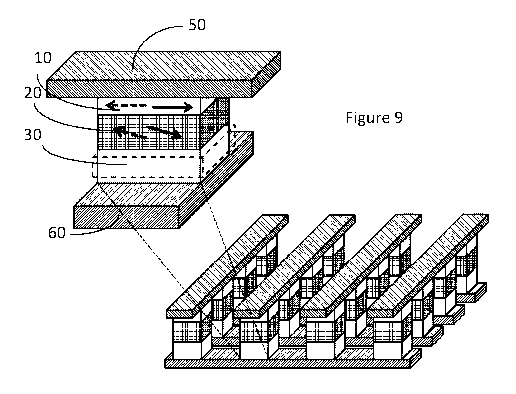
Figure 9 is a perspective schematic view of a two-dimensional array of
magnetic
memory cells according to an embodiment. As can be seen, a plurality of non-
volatile
memory cells according to the first or second embodiment are placed in a two-
dimensional
array. The first and second electrodes 50, 60 are in the form of strips. A
plurality of first
and second electrodes extend in orthogonal directions and each electrode is
connected to a
plurality of memory cells extending along the length of the electrode 50, 60.
Each memory
cell is thereby individually addressable by applying a potential difference
between
17
CA 03046162 2019-06-05
WO 2018/109441 PCT/GB2017/053674
electrodes 50 extending in a first direction and second electrodes 60
extending in the
orthogonal direction as described above for each embodiment (Figures 10 and 11
show
details of the potential difference applied in the first & third embodiments
and the second
embodiment, respectively). In this way, a densely packed two-dimensional non-
volatile
memory can be assembled in which individual memory cells are individually
addressable
and in which no transistors are needed for reading or writing data to the
individual memory
cells.
As explained above, in the first embodiment, magnetisation of the storage
layer 10
remains locked by the coercive field parallel (state 1) or antiparallel (state
0) to the small
magnetisation of the piezomagnetic layer 20. Each alignment state leads to a
different
magnetic state of the piezomagnetic layer 20 and thereby to different elastic
properties
which are detectable by magneto-capacitance measurement. This writing
mechanism
allows for addressing of individual bits integrated in an N-by-N array where
each bit is
connected to one of N top leads and to one of N bottom leads. The top and
bottom set of
leads are perpendicular to each other (cross-bar geometry), as illustrated in
Figure 9.
Figure 10 shows how to write the state of a memory bit of a memory cell
according to the
first embodiment (the same principles apply to the third embodiment, but with
the different
layered structure). DC-electric potentials Vtop and Vg are applied to the top
and bottom
leads contacting the memory cell of interest, respectively. A smaller DC-
potential (e.g.
V/3) is applied to the rest of the top leads and e.g. 2*Vt0p/3 is applied to
the rest of the
bottom leads. This results in a large voltage (Vtop, where Vg=0 is the ground)
at the
memory bit of interest which induces a strain in the piezomagnetic layer 20
which in turn
induces a magnetisation which is large enough to overcome the coercive field
of the
storage layer 10 and switch its magnetisation. All the other individual memory
cells of the
array are subject to a voltage which is only a third (2*Vtop/3-Vtop/3=Vtop/3)
of the switching
voltage (Vtop) so their state is not affected (a voltage below a threshold set
by the coercive
field).
In order to read information, as illustrated in Figure 12, a small AC-voltage
is
applied to the plates of the capacitor (piezomagnetic layer 20 and the bottom
contact layer
60) which is not large enough to induce a strain that could alter the magnetic
state of the
storage layer 10 but allows for a measurement of reactance and thereby of the
capacity of
the memory bit. The capacity depends on the relative permittivity and
dimensions of the
insulating strain-inducing layer 30, which in turn depends on the elastic
properties of the
piezomagnetic layer 20, which depend on the alignment of the magnetisation in
the storage
layer 10 (or 30 in scenario 3). This reading mechanism allows for addressing
of individual
18
CA 03046162 2019-06-05
WO 2018/109441 PCT/GB2017/053674
bits integrated in the N-by-N array described above. To read a memory bit, an
AC-voltage
is applied to the top and bottom leads contacting the relevant memory bit and
an AC-
voltage with opposite phase is applied to all leads not contacting the
relevant memory bit.
Thereby, at any point in time the voltage at any bit connected to the same
leads as the
relevant memory bit is zero and the voltage at any other bit is of the same
size but opposite
polarity as the voltage at the memory bit of interest. Therefore, the capacity
of the memory
bit of interest can be read without being affected by signal from other bits
connected to the
same leads and without affecting the memory state of any bit (non-destructive
readout).
Alternatively, the difference of magneto-capacitance between the two magnetic
states of the piezomagnetic layer can be determined as a shift of a resonance
frequency of a
circuit where the single memory cell is the capacitor and the inductor is in a
control unit
external to the memory array.
To write the state of a particular memory bit of the second embodiment in an N-
by-
N array with cross-bar geometry described above, DC-electrical potentials Vtop
and Vg are
applied to the top and bottom leads contacting the particular memory bit,
respectively as
illustrated in Figure 11. An opposite voltage is applied to all leads not
contacting the
particular memory bit (Vtop to the bottom leads and Vg to the top leads). This
results in a
large voltage (Vtop¨ Vg) at the particular memory bit which induces a strain
in the
piezomagnetic layer 20 which turns that layer paramagnetic so the particular
memory bit is
writable by an external magnetic field (not illustrated in Figure 11). All the
other memory
bits of the array are subject to zero voltage or the same voltage with
opposite polarity (Vg¨
so their Neel temperature is even higher above the ambient temperature and the
magnetisation of their storage layer is fixed.
The reading in the N-by-N array of the second embodiment is the same as in
case of
the first and third embodiment described with reference to figure 12.
In the third embodiment, writing is accomplished by applying a DC voltage as
in
case of the first embodiment. However this time the voltage must be large
enough to
switch a ferroelectric polarisation of a selected bit between a first and
second direction in
the ferroelectric layer 30 thereby to write data to the memory cell, the
ferroelectric
polarisation of the ferroelectric layer 30 in the first direction induces a
first magnetic state
in the antiperovskite piezomagnetic layer 20 and the ferroelectric
polarisation of the
ferroelectric layer 30 in the second direction induces a second magnetic state
in the
antiperovskite piezomagnetic layer 20; the voltage applied to the rest of the
bits is not
sufficient to switch their electric polarisation; the voltage is then removed
which does not
affect the ferroelectric polarisation. The read method comprises the steps of:
an AC voltage
19
CA 03046162 2019-06-05
WO 2018/109441 PCT/GB2017/053674
is applied to the 2D memory array as in the first type of embodiment as
illustrated in
Figure 12 to measure a magneto-capacitance of the selected memory cell, the
voltage
applied at any point in time to the rest of the cells connected to the same
leads is zero. The
magneto-capacitance of the selected memory bit is different in the first
magnetic state than
in the second magnetic state of the piezomagnetic layer, thereby allowing to
read the data
stored in the storage layer.
For all embodiments, because of the low lattice mismatch between individual
layers, it is possible to build a three-dimensional memory array using similar
principles in
which electrodes between layers of memory cells are used to address memory
cells on both
sides of that electrode. In order to be able to reach the electrodes passing
in the x-y
direction, the width of the layers in the x and y directions decreases with
height. Such a
memory is illustrated schematically in Figure 13.
Other arrangements of two and three-dimensional arrays are possible and within
the
scope of the skilled person.
The multilayers of this device can be manufactured using any thin film
deposition
method, optimised for the required layers. For example, a pulsed laser
deposition (PLD)
can be used. Example growth conditions for each thin film follow below.
Step 1: Substrate selection and cleaning.
Any suitable oxide substrate (e.g. MgO, SrTiO3, Nb:SrTiO3,
(LaA103)03(Sr2TaA106)07) or Si can be used as the substrate. The substrate is
cleaned with
a standard solvent clean procedure prior to the growth. The standard solvent
clean
procedure which may be a three-minute clean in an ultrasonic bath with
Acetone, then
Isopropanol and finally Distilled Water, with a N2 blow dry after each solvent
step. In an
embodiment, the substrate may become the bottom electrode 60.
Step 2: Multilayer Growth (PLD and Magnetron Sputtering).
Thin films are deposited by PLD using a KrF excimer laser (X-248 nm).
Stoichiometric single phase targets of SrRu03, Nb:SrTiO3, BaTiO3, BaxSri-
xTiO3,
BaZrxTi1,03, Mn3SnN and Mn3GaNrespectively, are ablated by a laser with
fluency of
0.8J/cm2 at 10 Hz.
Layer 1 ¨ Second Electrode 60 ¨ 100 nm SrRu03 thin film is grown at 700 C ¨
780 C under an 02 partial pressure of 50 ¨ 300 mTorr. After deposition, the
grown film is
CA 03046162 2019-06-05
WO 2018/109441 PCT/GB2017/053674
subsequently in-situ post-annealed for 20 minutes at the growth temperature
under an 02
partial pressure of 600 Torr. Then, the sample is cooled down to room
temperature at
C/min under an 02 partial pressure of 600 Torr.
Or 100 nm Nb:SrTiO3 thin film, grown at 700 C under an 02 partial pressure of
0 ¨
60 mTorr. After growth, the sample is cooled down to room temperature at 10
C/min under
an 02 partial pressure of 600 Torr.
Layer 2 ¨ Piezoelectric material of strain inducing layer 30 ¨ 100 nm
BaTiO3 (BaxSr1_xTiO3 or BaZrxTi1_,03) thin film is grown at 750 C ¨ 800 C
under an 02
partial pressure of 150 ¨ 300 mTorr. After growth, the sample is cooled down
to room
temperature at 10 C/min under an 02 partial pressure of 600 Torr.
Layer 3 ¨ Piezomagnetic layer 20 of Mn3XN, where X is any suitable element ¨
for
example, 100 nm Mn3SnN thin film is grown at 300 C ¨ 550 C under a N2 partial
pressure
of 0 ¨ 12 mTorr. After growth, the sample is cooled down to room temperature
at
10 C/min under a N2 partial pressure of 0 ¨ 12 mTorr.
Or 100 nm Mn3GaN grown at 300 C ¨ 550 C under a N2 partial pressure of 0 ¨ 12
mTorr. After growth, the sample is cooled down to room temperature at 10 C/min
under
the N2 partial pressure of 0 ¨ 12 mTorr.
Spacer Layer (only for embodiment 1) ¨ Perovskite paramagnet of non-magnetic
layer 15 ¨ a 1-2 nm Platinum (Pt) thin film is grown on a sample (comprised of
the
substrate, layers 60, 30, and 20) by DC magnetron sputtering. The sample is
heated to
800 C in ultra-high vacuum and annealed for 1 hour. Pt thin film is deposited
at 100W DC
power. After growth, the sample is cooled down to room temperature at 10 C/min
under
vacuum.
Layer 4 ¨ Ferromagnetic material of storage layer 10 - 20-50 nm Co3FeN thin
film is
grown at 300 C ¨ 500 C by RF magnetron sputtering from a Co3Fe target in 5-20
mTorr
Ar+N2 gas mixture atmosphere in which the volume concentration of N2 gas is in
a range
of 5 ¨ 15%. After growth, the sample is cooled down to room temperature at 10
C/min.
21
CA 03046162 2019-06-05
WO 2018/109441 PCT/GB2017/053674
Layer 5 ¨ First Electrode 50¨ 100 nm of a metal (for example Pt, Au) or a
conductive
perovskite thin film (for example SrRu03, Nb:SrTiO3).
100 nm Pt thin film is grown by DC magnetron sputtering. The sample is heated
to
800 C in ultra-high vacuum and annealed for 1 hour. Pt thin film is deposited
at 100W DC
power. After growth, the sample is cooled down to room temperature at 10 C/min
under
vacuum.
Or 100 nm SrRu03 thin film is grown at 700 C ¨ 780 C under an 02 partial
pressure of 50 ¨ 300 mTorr. After deposition, the grown film is subsequently
in-situ post-
annealed for 20 minutes at the growth temperature under an 02 partial pressure
of 600
Torr. Then, the sample is cooled down to room temperature at 10 C/min under
the 02
partial pressure of 600 Torr.
Or 100 nm Nb:SrTiO3 thin film, grown at 700 C under an 02 partial pressure of
0-
60 mTorr. After growth, the sample is cooled down to room temperature at 10
C/min under
an 02 partial pressure of 600 Torr.
Step 3: Photolithography.
A standard photolithography process has been implemented to apply an array
pattern. For 2D devices, all layers can be deposited and then patterned. For
3D stacking
device, each memory cell layer has to be patterned before the next layer is
deposited.
Step 4: Etching.
A standard Argon Ion Milling process to remove material and transfer the
pattern
from photolithography onto the sample, or any other suitable chemical or
physical etching
technique is implemented.
22