Note: Descriptions are shown in the official language in which they were submitted.
CA 03046200 2019-06-05
WO 2018/106761 PCT/US2017/064831
FREEZABLE FLUID CELL FOR CRYO-ELECTRON MICROSCOPY
CROSS-REFERENCES TO RELATED APPLICATIONS
[0001] This application is based on, claims the benefit of, and
incorporates herein by
reference, U.S. Provisional Patent Application 62/430,666, filed December 6,
2016.
STATEMENT REGARDING FEDERALLY SPONSORED RESEARCH
[0002] Not applicable.
TECHNICAL FIELD
[0003] This disclosure relates to cryo-electron microscopy and improved
fluid cells for
holding samples for cryo-electron microscopy.
BACKGROUND
[0004] Cryo-electron microscopy ("cryo-EM") is an imaging technique
performed on thin
films of vitrified aqueous samples. Cryo-EM is gaining popularity in
structural biology, and has
made it possible to observe the architecture of cells, viruses and protein
assemblies in their native
state at molecular resolution. Cryo-EM is based upon the principle of imaging
radiation-sensitive
specimen in a transmission electron microscope under cryogenic conditions and
high vacuum.
[0005] Plunge-freezing aqueous solutions into a cryogen, such as liquid
ethane, is a
common method used to prepare specimens for cryo-EM applications. Freezing
samples at
cryogenic temperatures reduces the extent of radiation damage that is caused
to the biological
sample. Specifically, electron irradiation leads to the breaking of chemical
bonds and the creation
of free radicals which, in turn, causes further damage to the sample. The
development of the
method to rapidly freeze or vitrify biological samples in thin-frozen layers
allows for the reduction
in radiation damage and for samples to be imaged with a higher radiation dose.
Additionally,
preserving the biological samples at cryogenic temperatures allows for the
preservation of the
biological sample under a high vacuum.
- 1 -
CA 03046200 2019-06-05
WO 2018/106761 PCT/US2017/064831
SUMMARY OF THE INVENTION
[0006] Disclosed herein is a system and method for imaging a biological
sample using a
freezable fluid cell for cryo-electron microscopy. As used herein, the term
"biological sample"
refers to a variety of macromolecule assemblies including, but not limited to,
protein molecules,
small peptides, individual bacteria, viruses, intact tissue sections, and
plunge-frozen cells. In the
disclosed methodology, an aqueous droplet containing a biological sample is
introduced into an
inlet port of the freezable fluid cell, in which the biological sample is
pulled into the device by
capillary action. The biological sample is then pulled into a thin, planar
fluid cell regime within
the cell. The freezable fluid cell is then rapidly cooled to immobilize the
biological sample in a
thin film of ice, which may alternatively be referred as a vitrified
biological sample. The thin film
can then be imaged using cryo-electron microscopy.
[0007] Previous approaches for imaging cryo-EM samples used robotic
blotting methods
for creating thin, vitrified biological samples which were often poorly
controlled. That is, robotic
blotting methods typically include depositing a few microliters of a purified
protein solution onto
a metal (usually copper) grid, on top of which lies a thin film of amorphous
carbon configured
with holes. A portion of the protein solution enters the holes of the
amorphous carbon grid, and
the remaining solution is blotted away using filter paper prior to plunge
freezing in liquid ethane.
These previous blotting methods resulted in frozen samples with variable ice
thicknesses due to
large air-liquid interfaces, and concentration gradients of the macromolecule
assemblies. The
variable ice thicknesses and concentration gradients necessitated time
intensive manual screening
of the vitrified biological sample to locate suitable regions for imaging.
Furthermore, the variable
ice thickness associated with previous blotting methods results in
inconsistent background noise
signals across the sample. Inconsistent background noise signals complicates
data post processing
and image reconstruction. This sample preparation stage of cryo-EM is widely
considered the
bottleneck in structure determination and an obstacle to automation of
structure determination.
[0008] The present disclosure addresses the aforementioned shortcomings
by providing a
freezable fluid cell to define the ice thickness of the biological sample. The
present disclosure also
removes the air-liquid interface that has been largely unavoidable using
robotic blotting methods,
which can be problematic in three-dimensional structure determination. By
removing the air-
liquid interface and plunge freezing the biological sample within a planar
fluid cell regime, the
- 2 -
CA 03046200 2019-06-05
WO 2018/106761 PCT/US2017/064831
present disclosure addresses the problem of variable ice thickness and poor
macromolecule
distribution.
[0009] The present disclosure also facilitates the automation process.
Previous methods
hindered automation for high-resolution cryo-EM imaging because traditional
blotting and plunge
freezing systems create ice thickness that varies across the substrate
surface. This necessitates
manual intervention to find areas that are sufficiently thin to obtain high-
resolution information,
yet not so thin that proteins are excluded from the ice. For example, thick
ice diminishes signal,
but if ice is too thin proteins will be pushed away. The present disclosure
facilitates automation
because it creates ice of customized and uniform ice thickness that also
accommodates the proteins.
As a consequence, a computer controlled imaging system can move from point to
point acquiring
images and the images will be of consistent quality because the ice thickness
is constant. Further,
the present disclosure also facilitates the automation process through a
regular array of imaging
windows.
[0010] According to one aspect, the present disclosure provides a
freezable fluid cell
system for cryo-electron microscopy. The freezable fluid cell system comprises
a top chip and a
bottom chip. The top chip includes a first structural member joined to a first
electron transparent
member. The bottom chip includes a second structural member joined to a second
electron
transparent member. The freezable fluid cell also includes a spacer positioned
between the top
chip and the bottom chip in which the spacer joins the top chip and the bottom
chip to define one
or more channels between the first electron transparent member and the second
electron
transparent member. The top chip further includes one or more inlet ports and
outlet ports that
extend through the first structural member and the first electron transparent
member such that the
inlet port, the outlet port, and the channel are in fluid communication. The
inlet port and the exit
port allow the freezable fluid cell device to be used and reused without
disassembly of the device.
[0011] Suitable materials for the first and second electron transparent
members may
include silica, silicon nitride, silicon carbide, graphene, or derivatives
thereof that are deposited
onto the respective first or second structural member. It is contemplated that
use of graphene or
silicon carbide may improve the image resolution by reducing the noise present
in the system.
[0012] In some forms, the first and second electron transparent members
each may have a
thickness that is 150 nm or less. In some non-limiting examples, the thickness
may range between
2 nm to 100 nm, or may range between 2 nm to 75 nm, or may range between 2 nm
to 50 nm, or
- 3 -
CA 03046200 2019-06-05
WO 2018/106761 PCT/US2017/064831
may range between 2 nm to 40 nm, or may range between 2 nm to 30 nm, or may
range between
2 nm to 20 nm, or may range between 2 nm to 10 nm, or may range between 2 nm
to 5 nm. It is
also contemplated the thickness of the first and second electron transparent
members may approach
an atomic thickness when using materials, such as, but not limited to
graphene. The atomic
thickness may be less than 2 nm, for example, the thickness may range between
0.4 nm to 1.7 nm,
which is approximately the thickness of a single layer of graphene. The
thickness for first and
second electron transparent members does not have to be the same.
[0013] In some forms, the first and second structural members may each
comprise silicon
and may each have a thickness of 500 p.m or less. In some non-limiting
examples, the thickness
of the first and second structural support members may range between 10 and
200 p.m, or between
20 and 180 p.m, or between 30 and 170 p.m, or between 40 and 160 p.m, or
between 50 and 150
p.m. Moreover, each of the first and second structural members may contain a
plurality of
trapezoidal recesses that extend through the respective one of the first or
structural member to form
respective first and second imaging windows on the surface of the respective
first and second
electron transparent member. The first and second imaging windows may each
have an area that
is less than 10 mm2. In one non-limiting example, the area of the imaging
windows may be
between 1 and 20 tm2.
[0014] In some forms, the spacer may comprise silicon oxide, indium, or
microparticle
beads and may have a thickness of 2 p.m or less. In some non-limiting
examples, the thickness of
the spacer 108 for cell biology applications may benefit from having the
thickness of the spacer
be around 1 p.m, while high-resolution protein imaging benefits from the
thickness of the spacer
108 being around 20 nm. In some configurations, the thickness of the spacer
108 may be between
20 nm and 1 p.m. In a preferred configuration, thickness of the spacer 108 may
be between 20 and
200 nm. In the case of indium, the thermal and electrical conductivity of
indium may facilitate
charge dissipation during imaging.
[0015] According to another aspect, the present disclosure also provides a
method for imaging a
biological sample using cryo-electron microscopy. A biological sample is
deposited into the inlet
channel of the freezable fluid cell system described above (which may have any
of the various
workable permutations in structure described herein) with the biological
sample filling the total
volume within the channel. The biological sample is then frozen to produce a
vitrified biological
sample. An electron beam is directed through the first electron transparent
member, the vitrified
- 4 -
CA 03046200 2019-06-05
WO 2018/106761 PCT/US2017/064831
biological sample, and the second electron transparent member. A collection of
images are
acquired and collectively processed using statistical methods.
[0016] In some forms, the statistical methods may include principal component
analysis,
multivariate analysis, or covariance analysis.
[0017] In some forms, the method may further include the steps of
acquiring a series of
images at different tilts relative to the direction of the incident electron
beam, processing the
images through an imaging filter, and computationally combining the images to
produce
tomograms and a three-dimensional image of the vitrified biological sample.
[0018] In some forms, the step of directing an electron beam and
processing the image may
further include, acquiring a series of images using a fluorescent microscope,
locating the position
of fluorescent biological samples, and merging the data from the fluorescent
images with the cryo-
EM images such that the fluorescent biological samples are identifiable within
the cryo-EM
images.
[0019] In some forms, the biological sample may include an aqueous
solution further
containing one or more virus, protein molecule, bacteria, or tissue samples.
[0020] The foregoing and other aspects and advantages of the invention
will appear from
the following description. In the description, reference is made to the
accompanying drawings
which form a part hereof, and in which there is shown by way of illustration a
preferred
embodiment of the invention. Such embodiment does not necessarily represent
the full scope of
the invention, however, and reference is made therefore to the claims and
herein for interpreting
the scope of the invention.
BRIEF DESCRIPTION OF DRAWINGS
[0021] FIG. 1A shows top and cross-sectional views of a top chip for a
freezable fluid
cell system.
[0022] FIG. 1B shows top and cross-sectional views of a spacer for the
freezable fluid
cell system.
[0023] FIG. 1C shows top and cross-sectional views of a bottom chip for
the freezable
fluid cell system.
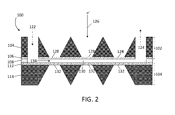
[0024] FIG. 2 shows a representative cross-sectional side view of an
assembled freezable
fluid cell system taken along 2-2 in FIGS. 1A, 1B, and 1C.
- 5 -
CA 03046200 2019-06-05
WO 2018/106761 PCT/US2017/064831
[0025] FIG. 3A shows an image of vesicular material from rotovirus VLP
preparation
taken from the freezable fluid cell system. The scale bar of the image is
approximately 100 nm.
[0026] FIG. 3B shows another image of vesicular material from rotovirus
VLP
preparation taken from the freezable fluid cell system.
[0027] FIG. 4A shows top and cross-sectional views of a top chip for a
freezable fluid
cell system.
[0028] FIG. 4B shows top and cross-sectional views of a spacer for the
freezable fluid
cell system.
[0029] FIG. 4C shows top and cross-sectional views of a bottom chip for
the freezable
fluid cell system.
[0030] FIG. 5 shows a schematic flow chart illustrating one non-limiting
example of a
method for reducing noise associated with a crystalline lattice in imaging
windows of the
freezable fluid cell.
[0031] FIG. 6 shows one non-limiting example of using the method of FIG.
5 on a single
crystal silicon imaging window. The following is shown: a real space image of
the single crystal
silicon imaging window (left), a reciprocal space image with diffraction spots
(left middle),
masks over the diffraction spots (right middle), and a corrected real image of
the single crystal
silicon imaging window with improved contrast (right).
[0032] FIG. 7 shows one non-limiting example of using the method of FIG.
5 on a single
crystal silicon imaging window having a gold nanoparticle in a imaging
channel. The following
is shown: a real space image of the single crystal silicon imaging window and
the gold
nanoparticle (left), a reciprocal space image with diffraction spots (left
middle), masks over the
diffraction spots (right middle), and a corrected real image of the single
crystal silicon imaging
window and the gold nanoparticle with improved contrast (right).
[0033] FIG. 8 shows a schematic flow chart illustrating one non-limiting
example of a
method to fabricate the freezable fluid cell system
DETAILED DESCRIPTION
[0034] Referring first to FIGS. 1A, 1B, 1C, and 2, one exemplary
embodiment of a
freezable fluid cell system 100 according to the present disclosure is shown.
The freezable fluid
cell system 100 comprises a top chip 102, a spacer 108, and a bottom chip 110.
In each of FIGS.
- 6 -
CA 03046200 2019-06-05
WO 2018/106761 PCT/US2017/064831
1A, 1B, and 1C, a top view along with a respective pair of cross sectional
side views for each
section (top, bottom, spacer) of the freezable fluid cell system 100 is
illustrated.
[0035]
In FIG. 1A, the top chip 102 of a freezable fluid cell system 100 is shown.
The
top chip 102 includes a first structural member 104 joined to a first electron
transparent member
106. The top chip 102 has at least one inlet port 122 and at least one exit
port 124 that extends
through the first structural member 104 and the first electron transparent
member 106 such that at
least one channel 134 within the spacer 108 (described in more detail below
and show in FIGS.
1B and 2) can remain in fluid communication with the inlet port 122 and the
exit port 124. The
top chip 102 also includes one or more imaging windows 128 that extend through
the first
structural member 104 to an exposed or uncovered section of the first electron
transparent member
106.
[0036]
Turning to FIG. 1C, the bottom chip 110 is shown. Similar to the top chip 102,
the
bottom chip 110 has a second structural member 114 and a second electron
transparent member
112. The second electron transparent member 112 joins the bottom chip 110 to
the spacer 108.
The bottom chip 110 also has one or more imaging windows 132 that extend
through the second
structural member 114 to an exposed or uncovered section of the first electron
transparent member
112. The imaging windows 128, 132 may include side walls that are vertical or
that have an inward
slope.
[0037]
Now with reference to FIGS. 1B and 2, the spacer 108 is positioned between the
top chip 102 and the bottom chip 110, with the spacer 108 providing structural
support, joining the
top chip 102 with the bottom chip 110, and defining a space therebetween. As
illustrated, the
spacer 108 has a plurality of openings formed therein that, along with the top
chip 102 and bottom
chip 110, defines one or more channels 134 into which the biological sample
130 can be drawn
into the freezable fluid cell system 100 by capillary forces through the inlet
port 122. The
biological sample 130 may then be frozen to establish a thin, vitrified film.
After imaging and
thawing of the sample, the sample may then be removed from the at least one
channel 134 within
the spacer 108 through the exit port 124 to be reused.
[0038]
As best illustrated in FIG. 2, during cryo-EM imaging, the electron beam 126
produced by a cryo-EM device will initially be directed through one or more of
imaging windows
128 in the top chip 102, pass through the frozen sample 130, pass through one
or more of imaging
windows 132, and be received by or collected one or more detectors. Data
collected by the detector
- 7 -
CA 03046200 2019-06-05
WO 2018/106761 PCT/US2017/064831
includes two-dimensional projections of biological molecules configured within
the biological
sample 130. Relative orientations of the individual particles can be
determined by processing the
two-dimensional projections using a computer to produce an image, i.e., a two-
dimensional or
three-dimensional structure of the biological molecule in the biological
sample 130. The two-
dimensional projections may be combined into a three-dimensional
reconstruction through the use
of computer hardware and software using methods known to those skilled in the
art.
[0039] During imaging of a biological sample 130, the most relevant
sources of
background noise within the freezable fluid cell system 100 can be attributed
to the ice thickness,
the first electron transparent member 106, and the second electron transparent
member 112. The
background noise within the freezable fluid cell system 100 therefore depends
on the thickness
and composition of each of these members.
[0040] In some forms, the first electron transparent member 106 and the
second electron
transparent member 112 can comprise a compound having a crystalline lattice.
For example, the
first electron transparent member 106 may comprise silicon nitride, silicon
carbide, graphene,
silica, derivatives or mixtures thereof Silicon carbide offers advantages
because the background
noise associated with silicon carbide can be computationally reduced in
reciprocal space during
post-processing. This is due to the characteristic solid crystalline lattice
of silicon carbide. This
offers benefits over silicon nitride, which contains an amorphous solid phase,
whose background
noise cannot be conveniently removed in post-processing steps. Similarly,
graphene also exhibits
a crystalline lattice, allowing for the background noise to be reduced in post-
processing steps.
Graphene also has an atomic thickness, and therefore contributes negligibly to
background noise
during image processing. In other configurations, the first electron
transparent layer 106 and the
second electron transparent layer 112 could include other allotropes of carbon
such as graphite,
charcoal, carbon nanotubes, and fullerenes. The first electron transparent
layer 106 and the second
electron transparent layer 112 may also be coated with a thin film. Suitable
thin film include, but
are not limited to, silicon nitride coatings.
[0041] In some configurations, the electron transparent members 106, 112
may have a
thickness that is 150 nm or less. As mentioned above, the thickness of the
electron transparent
members 106, 112 are significant contributors to background noise and
reduction of their thickness
while maintaining the structural integrity of the freezable fluid cell system
100 can help reduce
noise. In other configurations, the thickness of the electron transparent
members 106, 112 may
- 8 -
CA 03046200 2019-06-05
WO 2018/106761 PCT/US2017/064831
range between 2 nm to 100 nm, or may range between 2 nm to 75 nm, or may range
between 2 nm
to 50 nm, or may range between 2 nm to 40 nm, or may range between 2 nm to 30
nm, or may
range between 2 nm to 20 nm, or may range between 2 nm to 10 nm, or may range
between 2 nm
to 5 nm. It is also contemplated the thickness of the first and second
electron transparent members
may approach an atomic thickness when using materials, such as, but not
limited to graphene. The
atomic thickness may be less than 2 nm, for example, the thickness may range
between 0.4 nm to
1.7 nm, which is approximately the thickness of a single layer of graphene.
The thickness for each
of the electron transparent members 106, 112 does not have to be the same. The
first and second
imaging windows 128, 132 may each have an area that is less than 10 mm2. In
one non-limiting
example, the area of the imaging windows may between 1 and 20 tm2.
[0042] It is to be appreciated that the term "electron transparent" as
used herein does not
require the electron transparent members to be 100% transparent. Rather, any
material that permits
an adequate proportion of the electron beam 126 to pass through the electron
transparent members
to allow for an image to be acquired may be used.
[0043] Suitable materials for the first structural support member 104 and
the second
structural support member 114 may include silicon, silicon dioxide, gold,
derivatives or mixtures
thereof. The thickness of the structural support members 104 and 114 may be
500 p.m or less. In
some non-limiting examples, the thickness of the structural support members
104 and 114 may
range between 10 and 200 p.m, or between 20 and 180 p.m, or between 30 and 170
p.m, or between
40 and 160 p.m, or between 50 and 150 p.m. In other configurations, suitable
materials for the
structural support members 104, 114 may comprise a synthetic organic or
inorganic polymer such
as, but not limited to polyethylene, polypropylene, polyvinyl chloride,
polystyrene, nylon, Teflon,
thermoplastic polyurethanes, and derivatives thereof
[0044] In some configurations, suitable materials for the spacer 108 may
comprise silicon
oxide, aluminum oxide, aluminum silicate, gallium, or indium. In one
particular configuration,
the spacer 108 comprises silicon dioxide or indium. Indium can offer several
advantages over
silicon dioxide. First, indium has a suitable electrical conductivity that can
facilitate charge
dissipation during imaging. Second, indium has a higher density and provides
improved structural
integrity for the freezable fluid cell system 100. Third, the low temperature
thermal evaporation
of indium simplifies the patterning of indium and its thickness control onto
the bottom chip during
manufacturing.
- 9 -
CA 03046200 2019-06-05
WO 2018/106761 PCT/US2017/064831
[0045] As mentioned above, the thickness of the spacer 108 defines and
ultimately
corresponds to the thickness of the vitrified biological sample 130, which
thickness contributes to
the background noise within the freezable fluid cell system 100. Accordingly,
it is desirable to
minimize the thickness of the spacer 108 while maintaining structural
integrity. However, it is to
be appreciated that different biological imaging applications benefit from
different thicknesses of
the spacer 108. In some forms, the thickness of the spacer may be 2 p.m or
less. In some non-
limiting examples, the thickness of the spacer 108 for cell biology
applications may benefit from
having the thickness of the spacer be around 1 p.m, while high-resolution
protein imaging benefits
from the thickness of the spacer 108 being around 20 nm. In some
configurations, the thickness
of the spacer 108 may be between 20 nm and 1 p.m. In a preferred
configuration, thickness of the
spacer 108 may be between 20 and 200 nm.
[0046] In some forms, the spacer 108 may comprise microparticle beads 408
as depicted
in FIGS. 4A, 4B, and 4C. This embodiment parallels the freezable fluid cell
100 disclosed in
FIGS. 1A, 1B, and 1C. In this configuration, the microparticle beads 408 are
positioned such that
each of the four corners of the top chip 402 and bottom chip 410 are joined by
the microparticle
beads 408. Similar to above, the microparticle beads 408 may be made of
silicon oxide, aluminum
oxide, aluminum silicate, gallium, or indium. In this configuration, the
microparticle beads 408
do not cover the entire periphery between top chip 402 and bottom chip 410.
Therefore, the interior
space 434 of the freezable fluid cell device 400 for encapsulating the
biological sample 430 will
have an open interface to air along four sidewalls with a thickness defined by
the microparticle
beads. In this configuration, the biological sample 430 is loaded by capillary
action along the open
interfaces.
[0047] In one aspect, the microparticle beads 408 do not bond the top
chip 402 to the
bottom chip 410, rather the microparticle beads are placed in the corners of
the bottom chip 410
followed by the placement of the top chip 402 on top of the microparticle
beads 408 to assemble
the freezable fluid device 400. This allows for the freezable fluid device 400
to be disassembled
and for each of the components to be easily washed between trials.
Microparticle beads 408 can
be particularly advantageous for certain biological samples 430. In
particular, the open interface
allows air to be in contact with the biological sample 430, which allows cells
to grow inside of the
freezable fluid cell device 400. In this case, cells are seeded inside of the
freezable fluid cell device
400 and immersed in cell culture media. The open interface then allows for
nutrients in the cell
- 10 -
CA 03046200 2019-06-05
WO 2018/106761 PCT/US2017/064831
culture media to diffuse into the freezable fluid chamber to enable the cells
to grow. Once the
cells are sufficiently grown, the device is removed and plunge frozen for
imaging as described
above.
[0048] With reference to FIG. 3, a non-limiting image of the biological
sample 130 taken
with the freezable fluid cell system 100 is shown. Specifically, FIG 3 shows a
vesicular material
observed in a rotavirus VLP preparation, imaged with the freezable fluid cell
system 100 after
plunge freezing in liquid ethane. An advantageous aspect of the freezable
fluid cell system 100 is
that the uniformly defined ice layer formed upon freezing the fluid cell, and
high contrast at the
first imaging window 128 edge (i.e. where the first electron transparent
member 106 overlaps with
tapered edge of the first structural member 104) makes the device amenable to
automated data
collection. Automation is currently used in cryo-EM, but high-resolution work
is hampered
because resulting data is of inconsistent quality owing to lack of uniformity
in the ice layer on
standard cryo-EM systems.
[0049] In addition to unimodal cryo-EM imaging of cells and proteins, the
freezable fluid
cell system 100 could be used for multimodal correlative imaging with
fluorescence light
microscopy and cryo-EM. For example, the freezable fluid cell system 100 could
be populated
with a mixture of fluorescent and non-fluorescent proteins, frozen, and then
imaged with a
fluorescent microscope to localize the fluorescent proteins. Cryo-EM imaging
could then be done,
and then data from both imaging modalities merged to identify the fluorescent
molecules in the
cryo-EM image data (i.e. cryo-EM data does not capture fluorescence but can be
augmented with
data from the fluorescent light microscope). Alternatively, this same approach
could be adopted
with cells expressing fluorescent proteins of interest. After protein
localization with the fluorescent
microscope, the proteins could be localized in the electron microscope and
micrographs or
tomograms acquired.
[0050] The present disclosure also pertains to a method of using the
freezable fluid cell
system 100 to image a biological sample 130 using cryo-EM. First, the
biological sample 130 is
deposited into the inlet port 122 of the freezable fluid cell system 100. The
biological sample 130
is deposited such that it fills the total volume of the at least one channels
134 of the spacer 108.
The freezable fluid cell system 100 is then cooled to produce a vitrified
biological sample 130.
The vitrified biological sample is formed such that it is of uniform thickness
along the length of
the at least one channels 134, and so that no air interface exists between the
vitrified biological
- 11 -
CA 03046200 2019-06-05
WO 2018/106761 PCT/US2017/064831
sample 130 and either of the electron transparent members 106, 112. Next, an
electron beam is
directed through the first electron transparent member 106, the vitrified
biological sample 130, and
the second electron transparent member 112. Finally, the image is processed
using statistical
methods.
[0051] In some configurations, cooling the biological sample 130 involves
plunge freezing
into a cryogen, such as liquid ethane cooled by liquid nitrogen. Alternatives
to the cryogen could
include liquid propane. The methods disclosed above are not limited to two-
dimensional imaging,
but could include three-dimensional imaging. To collect three-dimensional
images of the
biological sample 130, a series of images are collected, with each image taken
at a different tilt
relative to the direction of the incident electron beam 126. Images are then
combined
computationally, to generate tomograms. Averaging methods can then be employed
to obtain more
detailed structural information. If the structure is morphologically
heterogeneous, multiple
tomograms may be used to identify patterns in structural variation.
[0052] In some forms, imaging the biological sample 130 using cryo-EM
includes a
method 500 for reducing noise associated with the crystalline lattice of the
imaging windows 128,
132. Referring to FIG. 5, the method 500 includes acquiring a real space image
502, i.e. a TEM
image, of the imaging windows 128, 132 in the freezable fluid cell system 100.
A reciprocal space
image 504 is then produced from the real space image by applying, for example,
a Fourier
transform or a diffraction pattern analysis, such as, but not limited to, a
Gatan program or the like.
The reciprocal space image 504 comprises diffraction spots associated with the
crystalline lattice
of the imaging windows 128, 132 that may be identified and masked using a
noise reduction
operation 506. The noise reduction operation 506 may include, for example,
employing Gaussian
shaped soft-edged masks in reciprocal space to suppress certain frequency
ranges.
[0053] A corrected real image 508 is then generated from the masked
reciprocal space
image by, for example, taking the inverse Fourier transform of the masked
reciprocal space image.
To further illustrate the method 500, FIG. 6 shows one non-liming example of
reducing noise
associated with a crystalline lattice in a single crystal silicon imaging
window. The single crystal
silicon imaging window illustrated in FIG. 6 has a thickness of 35 nm, and is
deposited on a silicon
structural member having a 100 p.m thickness. A real space image of the single
crystal silicon
imaging window (left) is shown taken from a <1-0-0> orientation for
diffraction studies. FIG. 6
further illustrates a reciprocal space image with diffraction spots evident
(left middle). The
- 12 -
CA 03046200 2019-06-05
WO 2018/106761 PCT/US2017/064831
reciprocal space image is generated from the real space image using a fast
Fourier transform
diffraction pattern analysis with Gatan programing. Diffraction patterns of
the single crystal
silicon imaging window are identified and masked as shown in FIG. 6 (right
middle). A corrected
real space image (right) is then generated by applying an inverse fast Fourier
transform to reduce
the signal associated with the single crystal silicon imagine window. Reducing
the noise
associated with the crystalline lattice of the imaging window produces a real
image with improved
contrast.
[0054] FIG. 7 illustrates another non-limiting example of reducing noise
associated with a
crystalline lattice in a single crystal silicon imaging window having a gold
nanoparticle in the
imaging channel. The single crystal silicon imaging window illustrated in FIG.
7 has a thickness
of 35 nm, and is deposited on a silicon structural member having a 100 p.m
thickness. A real space
image of the single crystal silicon imaging window and the gold nanoparticle
(left) is shown taken
from a <1-0-0> orientation for diffraction studies. FIG. 7 further illustrates
a reciprocal space
image with diffraction spots evident (left middle). The reciprocal space image
is generated from
the real space image using a fast Fourier transform diffraction pattern
analysis with Gatan
programing. Diffraction patterns of the single crystal silicon imaging window
are identified and
masked as shown in FIG. 7 (right middle). A corrected real space image (right)
is then generated
by applying an inverse fast Fourier transform to reduce the signal associated
with the single crystal
silicon imagine window. The corrected real space image (right) includes
improved contrast over
the real space image (left).
[0055] Although FIGS. 6-7 illustrate a method for reducing noise
associated with the
crystalline lattice of a single imaging window; however, the method 500 could
be performed on a
freezable fluid cell system 100 having a first imaging window 128 and a second
imaging window
132. That is, background noise attributed to the crystalline lattice of both
imaging windows 128,
132 could be reduced simultaneously by identifying and masking independent
diffraction patterns
using a method similar to the one described above.
[0056] Referring to FIG. 8 a flowchart is provided for one implementation
of a method
800 for fabricating a freezable fluid cell system 100 in accordance with the
present disclosure, for
example from a top chip 102 and a bottom chip 110. Initially during
fabrication, the top chip 102
and the bottom chip 110 may be provided as substantially planar substrates
having multiple layers.
For example, as described above, the top chip 102 may include a first
structural member 104 joined
- 13 -
CA 03046200 2019-06-05
WO 2018/106761 PCT/US2017/064831
to a first electron transparent member 106, and the bottom chip 110 may
include a second structural
member 114 joined to a second electron transparent member 112.
[0057] The method 800 further includes patterning the top chip 806 to
form an inlet port
122, an exit port 124, and a first imaging window 128 in the first structural
member 104 and the
first electron transparent member 106. In some aspects, the method 800
includes an optional step
of depositing a masking agent 804 onto portions of the top chip 102, i.e. the
first structural member
104 and the first electron transparent member 106, to protect regions of
interest during etching.
As used herein, a "masking agent" refers to a material that may be photo-
resistant or chemical-
resistant to etching agents. Suitable masking agents for the present
disclosure include durable
materials such as silicon nitride and derivatives thereof
[0058] Suitable patterning techniques for the present disclosure may
include
photolithography, dry etching, wet etching, or similar techniques known in the
art to etch portions
of a thin film from a bulk substrate. In one non-limiting example, wet etching
techniques such as
buffered oxide etching (BOE) or tetramethylammonium hydroxide (TMAH) are
performed to
pattern regions of interest on the substrate. Suitable deposition techniques
for the present
disclosure may include chemical deposition and physical deposition methods.
Non-limiting
deposition methods may include, for example, chemical vapor deposition (CVD),
atomic layer
deposition (ALD), physical vapor deposition (PVD), sputtering, or similar
methods.
[0059] The method 800 further includes patterning the bottom chip 810 to
form a second
imaging window 132 in the second structural member 114. Similar to above,
patterning the bottom
chip 810 may include an optional step of depositing a masking agent 808 onto
portions of the
bottom chip 110, i.e. the second structural member 114 and the second electron
transparent
member 112, to protect regions of interest during etching. After patterning, a
spacer 108 may be
deposited 810 onto either the top chip 102 or the bottom chip 110. In one non-
limiting example,
the spacer 108 may be deposited onto the first electron transparent member 106
or the second
electron transparent member 112. After deposition, the method 800 further
includes coupling the
spacer 812 to the top chip 102 and the bottom chip 110 to form a channel 134
in fluid
communication with the inlet port 122 and the exit port 124. As used herein,
"coupling" may refer
to chemically bonding the spacer 108 to the top chip 102 and the bottom chip
110, or it may refer
to placing the spacer 108 into contact with the top chip 102 and the bottom
chip 110.
- 14 -
CA 03046200 2019-06-05
WO 2018/106761 PCT/US2017/064831
[0060] It should be appreciated that various other modifications and
variations to the preferred
embodiments can be made within the spirit and scope of the invention.
Therefore, the invention
should not be limited to the described embodiments. To ascertain the full
scope of the invention,
the following claims should be referenced.
- 15 -