Note: Descriptions are shown in the official language in which they were submitted.
Title
PIXEL UNIT STRUCTURE AND MANUFACTURING METHOD THEREOF
Background of the Invention
1. Field of the Invention
[0001] The present invention relates to a pixel unit structure and
a manufacturing method thereof, and more specifically, the present
invention relates to a pixel unit structure with a display medium
module and a manufacturing method thereof.
2. Description of the Prior Art
[0002] With the advancement of technology, users are getting more
demanding about visual display and require display devices with the
advantages of compactness, excellent display quality, large-sized
panel, high color saturation, low cost and low power consumption.
(0003] Existing display devices maybe categorized into self-luminous
and non-self-luminous ones. Liquid crystal display (LCD) devices are
one of the primary non-self-luminous flat panel display devices,
wherein the amount of light passing through a liquid crystal medium
is modulated by controlling the voltage of the upper and lower
electrodes of the liquid crystal medium. The effect of color display
is achieved with further employment of a color filter layer, a
polarizer and some optical films.
[0004] Self-luminous flat panel display devices may be categorized
into field emissive display, plasma display, electroluminescent
display, organic light-emitting diode display and so on. In an organic
light-emitting diode display (OLED), light-emitting polymers are
deposited between an upper electrode layer and a lower electrode layer.
With further employment of a conductive layer of electrons and holes,
light is generated by means of an external electric field which moves
the carriers and causes the electrons and holes to re-combine. In
comparison, an organic light-emitting diode display device is
characterized by its wide viewing angle, fast responding speed, thin
1
DateRecue/DateReceived2023-10-26
panel and flexibility; further, it requires neither backlighting nor color
filter and may be made
large-sized.
[0005] The display panel of both LCD and OLED devices has a plate of
transparent glass for a
substrate, directly forming a thin-film transistor, a lower electrode layer, a
display medium layer,
an upper electrode layer and others thereon. The thin-film transistor may
control the voltage or
current imposed on the upper electrode layer and/or the lower electrode layer
to control the state of
the display medium.
[0006] However, a glass substrate may not endure a high annealing temperature
(the strain
temperature of glass being around 650 C). Therefore, the manufacturing process
of the foregoing
elements has to be performed at a relatively low temperature. This may cause a
low mobility rate
of electron in the thin-film transistor, which means a larger-sized transistor
is required for
providing sufficient charging ability.
[0007] Further, thelargerthesizeofthegl asssubstrate, thelarger the area of
the thin-film transistor
formed on the glass substrate (that is, thearray ofthethin-film transistor has
largerdimensions). The
manufacturing process of the thin-film transistor will have the disadvantages
of expensive
equipment, complicated manufacturing process, longer manufacturing time, and
unstable mass
production quality and yield rate. Therefore, a large-dimensioned array of
thin-film transistor is
harder to manufacture and its manufacturing cost is higher.
[0008] In view of the foregoing, existing display devices still have various
disadvantages to
overcome.
Summary of the Invention
According to an aspect of the invention, there is provided a display device
comprising: a housing
structure; and a plurality of pixel unit structures, independently assembled
with the housing structure,
each of the pixel unit structures comprising: a display medium module
comprising a first electrode
disposed on a first substrate, a second electrode and a display medium,
wherein the first electrode and
the second electrode are separated from each other, and the display medium is
disposed between the
first electrode and the second electrode; and an active switching element
electrically connected to the first
2
Date Recue/Date Received 2023-10-26
electrode for allowing the first electrode and the second electrode to change
the state of the display
medium, and wherein the active switching element includes a chip part and a
transistor portion with the
transistor portion formed on the chip part; wherein each of the pixel unit
structures is independently
disassembled from the housing structure and replaced with another pixel unit
structure.
According to another aspect of the invention, there is provided a pixel unit
structure, comprising: a
display medium module comprising a first electrode disposed on a first
substrate, a second electrode and
a display medium, wherein the first electrode and the second electrode are
separated from each other,
and the display medium is disposed between the first electrode and the second
electrode; and an active
switching element electrically connected to the first electrode for allowing
the first electrode and the
second electrode to change the state of the display medium, and wherein the
active switching element
includes a chip part and a transistor portion with the transistor portion
formed on the chip part; wherein no
element of the pixel unit structure is connected to and/or integrated with any
element of another pixel unit
structure.
[0009] It is a primary aspect of the present invention to provide a pixel unit
structure and a
manufacturing method thereof, wherein the
2a
Date Recue/Date Received 2023-10-26
pixel unit structure may be applied in a display device to improve
one of the disadvantages of existing display devices, for example,
to improve the manufacturing yield rate, lower the manufacturing cost,
reduce the manufacturing time, or improve the mobility rate of
electron, and so on.
[0010] To achieve the foregoing object, the present invention
provides a pixel unit structure comprising a display medium module
and an active switching element. The display medium module comprises
a first electrode, a second electrode and a display medium. The first
electrode and the second electrode are separated from each other,
and the display medium is disposed between the first electrode and
the second electrode. The active switching element is electrically
connected to the first electrode for allowing the first electrode
and the second electrode to change the state of the display medium.
The active switching element comprises a chip part and a transistor
portion, with the transistor portion formed on the chip part.
[0011] To achieve the foregoing object, the present invention
provides a manufacturing method for manufacturing a pixel unit
structure according to the present invention, comprising the
following steps: separately manufacture a display medium module and
an active switching element; assemble the active switching element
on the display medium module; wherein the display medium module
comprises a first electrode, a second electrode and a display medium,
the first electrode and the second electrode are separated from each
other, the display medium is disposed between the first electrode
and the second electrode, the active switching element comprises a
chip part and a transistor portion with the transistor portion formed
on the chip part, and the active switching element is electrically
connected to the first electrode for allowing the first electrode
and the second electrode to change the state of the display medium.
[0012] Thus, a pixel unit structure and a manufacturing method thereof
according to the present invention may provide at least the following
3
Date Recue/Date Received 2023-10-26
advantageous effects: the active switching element is manufactured
before being assembled on the display medium module; that is, the
active switching element is not directly manufactured on some portion
of the display medium module. As such, the manufacturing process
condition of the active switching element may be less restricted by
the characteristics of the display medium module (e.g. material
property). Further, the active switching element is manufactured on
a wafer, which may endure a higher processing temperature, and the
processing technique of wafers is also more matured and advanced.
Therefore, active switching elements manufactured on wafers may have
better characteristics (e.g. a higher yield rate or a faster mobility
rate of electron in a transistor).
[0013] On the other hand, the pixel unit structure maybe independently
disposed, assembled and disassembled. In the case of a display panel
composed of a plurality of pixel unit structures, a damaged pixel
unit structure may be disassembled and replaced by a new one. As such,
there is no need to replace an entire display panel for the sake of
a single damaged pixel unit structure.
[0014] The foregoing objects, technical features and advantages of
the present invention will become apparent after the following
detailed description of preferred embodiments in conjunction with
the attached drawings.
[0015] These and other objectives of the present invention will no
doubt become obvious to those of ordinary skill in the art after
reading the following detailed description of the preferred
embodiment that is illustrated in the various figures and drawings.
Brief Description of the Drawings
[0016] Figure 1 is a top view of a pixel unit structure according to
a first preferred embodiment of the present invention;
[0017] Figures 2A and 2B are cross-section views of the pixel unit
4
Date Recue/Date Received 2023-10-26
structure of Figure 1;
[0018] Figures 3A to 3C are cross-section views of a pixel unit
structure according to a second preferred embodiment of the present
invention;
[0019] Figures 4A and 4B are cross-section views of a pixel unit
structure according to a third preferred embodiment of the present
invention;
[0020] Figures SA and 5B are cross-section views of a pixel unit
structure according to a fourth preferred embodiment of the present
invention;
[0021] Figure 6 is a flow diagram showing a manufacturing method of
a pixel unit structure according to a fifth preferred embodiment of
the present invention;
[0022] Figure 7A is a three-dimensional view of a display device
according to a sixth preferred embodiment of the present invention;
[0023] Figure 7B is a detailed drawing showing the display device of
Figure 7A in partial enlargement;
[0024] Figure 7C is a partial cross-section view of the display device
of Figure 7A; and
[0025] Figure 8 is an application schematic view of the display device
of Figure 7A.
Detailed Description
[0026] The implementation method of the present invention will be
further illustrated by way of the following description of six
preferred embodiments. But it should be noted that the six preferred
embodiments described below are illustrative and exemplary only
rather than limiting the application of the present invention to the
described environment, application, structure, procedure or steps.
Elements that are not directly related to the present invention are
ignored from the drawings. The scale relations among elements in the
drawings are illustrated rather than limiting of the actual scales
of the present invention. Unless noted otherwise, identical (or
similar) reference symbols correspond to identical (or similar)
elements.
Date Recue/Date Received 2023-10-26
[0027] Please refer to Figure 1, showing a top view of a pixel unit
structure lA according to a first preferred embodiment of the present
invention. The pixel unit structure lA may serve as part of a display
panel (not shown in the drawing) for displaying a pixel part of an
image; that is, a display panel may include one or a plurality of
pixel unit structures lA according to the present embodiment. The
pixel unit structure lA may include an active switching element 13,
a display medium module 15 and other elements. The active switching
element 13 may be used to control the state of the display medium
module 15 to further control the amount of light passing through a
display medium module 15 (or modulating the properties of light)
More specific technical contents will be illustrated below.
[0028] Please refer to both Figures 2A and 2B, showing cross-section
views of the pixel unit structure lA of Figure 1. The active switching
element 13 may include a chip part 133 and a transistor portion 135,
with the transistor portion 135 formed on the chip part 133. That
is, the chip part 133 is part of a wafer (not shown in the drawings).
The wafer may be silicon wafer, gallium arsenide wafer, sapphire wafer,
indium phosphide wafer or gallium nitride wafer and so on (silicon
wafer is used in the present preferred embodiment). The transistor
portion 135 is formed on the wafer by a semiconductor manufacturing
process (exposure, development, etching, diffusion, deposition, and
so on). A plurality of transistor portions 135 may be simultaneously
formed on the wafer and then the wafer maybe divided into a plurality
of parts by a cutting process (with each part including one or more
transistor portions 135). Each of these parts is a foregoing active
switching element 13. The active switching element 13 may also be
regarded as a chip or die.
[0029] Further, the transistor portion 135 may be formed of one of
the following semiconductor materials: silicon, silicon on insulator
(SOI), germanium, selenium, gallium arsenide, gallium nitride,
three-five compound, two-six compound, four-four compound, four-four
6
Date Recue/Date Received 2023-10-26
alloy, amorphous silicon, and a combination thereof. In addition,
the active switching element 13 may also include a plurality of
electrodes 137 formed on the chip part 133 and/or the transistor
portion 135 for electrically connecting to the source electrode, gate
electrode and drain electrode of the transistor portion 135
separately.
[0030] The display medium module 15 comprises a first electrode 151,
a second electrode 153 and a display medium 155. The first electrode
151 and the second electrode 153 are separated from each other and
may face each other. And the display medium 155 is disposed between
the first electrode 151 and the second electrode 153. The first
electrode 151 and the second electrode 153 may also be called pixel
electrode and common electrode and may be transparent electrodes (e.g.
formed of indium tin oxide). Electrical energy may be imposed on the
first electrode 151 and the second electrode 153 to change the
magnitude and/or the direction of the voltage, current, inductance,
capacitance, electrical field, and magnetic field between the first
electrode 151 and the second electrode 153 and one of the combinations
thereof.
[0031] The first electrode 151 may also be electrically connected to
the active switching element 13 (e.g. via the electrode 137 of the
active switching element 13). The active switching element 13 may
control whether electrical energy is to be imposed on the first
electrode 151 and/or the second electrode 153.
[0032] The display medium 155 may also be called light modulation
medium. Its state may be changed via the first electrode 151 and the
second electrode 153 to control the amount of light passing through
(or modulate the properties of light). Specifically, the active
switching element 13 may control the electrical energy imposed on
the first electrode 151 and/or the second electrodes 153, causing
the voltage and so on between the first electrode 151 and the second
electrode 153 to change, which causes the state of the display medium
7
Date Recue/Date Received 2023-10-26
155 to change. Inthe case of a display medium 155 made of non-self-
luminous liquid crystal, change in the state of the display medium 155
means torsion of the liquid crystal. In the case of a display medium 155
made of self-luminous organic light-emitting diode, change in the state of
the display medium 155 means light generation of the organic light-
emitting diode. The type of the display medium 155 is relevant to the
configuration of the first electrode 151andthe second electrode 153. For
example, if the display medium 155 is in-plane-switching liquid crystal, the
first electrode 151 and the second electrode 153 may be arranged on the
same plane.
[0033] Besides non-self-luminous and self-luminous medium materials, in
other preferred embodiments the display medium 155 may also include
color filter material, conductive material, insulating material, light
absorbing material, light reflecting material, photo refractive material,
light
deflecting material, light diffusing material and at least one of the
foregoing
materials (the foregoing materials may be formed on thefirst substrate 157A
and/or the second substrate 157B described below, or maybe formed into a
plate body before being disposed on the first substrate 157A and/or the
second substrate 157B). Non-self-luminous medium materials may include
at least one of electrophoretic material, electric fluid material, liquid
crystal
material, micro electromechanical reflective material, electrowetting
material, electric ink material, magnetic fluid material, electrochromic
material, electromorphous material and thermochrornic material. Self-
luminous medium materials may include at least one of electroluminescent
material, photoluminescent material, cathodoluminescent material, field
emissive luminescent material, vacuum fluorescent material and light-
emitting diode material for producing white, red, green, blue, orange,
yellow and other colors, or combinations thereof.
[0034] The display medium module 15 may also include a first substrate
157A and a second substrate 157B, which are disposed facing each other
and separate from each other and are used for supporting the first
8
Date Recue/Date Received 2023-10-26
electrode 151, the second electrode 153 and/or the display medium
155. The first electrode 151 may be disposed on the first substrate
157A, the second electrode 153 may be disposed on the first substrate
157A and/or the second substrate 157B (depending on the type of the
display medium 155), and the display medium 155 may be disposed between
the first substrate 157A and the second substrate 157B (or, when the
display medium module 15 comprises only one of the first substrate
157A and the second substrate 157B, the display medium 155 may be
disposed on the first substrate 157A or the second substrate 157B).
The active switching element 13 may be disposed on the first substrate
157A and/or the second substrate 157B, but not directly manufactured
on the first substrate 157A and/or the second substrate 157B; that
is, the active switching element 13 is manufactured before being
assembled to the first substrate 157A and/or the second substrate
157B. Further, the active switching element 13 may be disposed on
a surface of the first substrate 157A and/or the second substrate
157B.
[0035] The first substrate 157A or the second substrate 157B may be
made of (but not limited to) the following materials: transparent
material, opaque material, flexible material, rigid material,
metallic material, ceramic material, insulating material, metal
compound material, metal alloy material, organic material, inorganic
material, composite material, semiconductor material and one of the
combinations thereof. In the present preferred embodiment, the first
substrate 157A and the second substrate 157B are made of transparent
material (such as glass).
[0036] The foregoing flexible material may include: polyethylene
naphthalate (PEN), polyvinyl chloride (PVC), polyether sulfone (PES),
polyethylene terephthalt (PET), polyarylate (PAR), polystyrene (PS),
polycarbonate (PC), polyimide (PI), polymethyl methacrylate (PMMA),
polyacrylonitrile (PAN), polyamide (PA) and one of the combinations
thereof.
9
Date Recue/Date Received 2023-10-26
[0037] The pixel unit structure lA may also include a control signal line
17 and a data signal line 19. The control signal line 17 and the data
signal line 19 maybe formed on the first substrate 157A and/or the second
substrate 157B and electrically connected to the active switching element
13 (e.g. via the electrode 137of the active switching element 13). The on
and off of the active switching element 13 may be controlled via the
control signal line 17, and electrical energy (i.e. pixel content, which
is represented in the form of voltage or electric current) may optionally
be transmitted to the active switching element 13 via the data signal line
19andbe further imposed on the first electrode 151. The control signal
line 17, data signal line 19, first electrode 151and/or second electrode
153 may be located on a same horizontal layer or on different horizontal
layers of the first substrate 157A and/or the second substrate 157B.
[0038] Further, the control signal line 17, data signal line 19, first
electrode 151 and/or second electrode 153 maybe made of (but not limited
to) the following materials: transparent conductive material, non-
transparent conductive material, flexible conductive material, rigid
conductive material, metallic conductive material, metal compound
material, metal alloy material, organic conductive material, inorganic
conductive material, and composite conductive material, and one of the
combinations thereof.
[0039] As illustrated above, the active switching element 13 is made from
a wafer and not directly formed on some portion of the display medium
module 15. Therefore, the manufacturing of the active switching element 13
may not be restricted by the characteristics of the display medium module
15. In addition, when the active switching element 13 is manufactured on a
wafer, since wafers may endure a higher processing temperature, and since
wafer processing technique is more matured and advanced, the active
switching element 13 manufactured on a wafer may have better
characteristics (e.g. of a smaller size, with a higher yield rate or a
faster mobility rate in a transistor).
Date Recue/Date Received 2023-10-26
[0040] Further, it has been noted above that the display panel (not
shown in the drawings) may include a plurality of pixel unit structures
1A. In this type of configuration, the first substrate 157A of the
display medium module 15 in these pixel unit structures lA may be
connected and integrated and so may the second substrate 157B. One
of the first electrode 151 and the second electrode 153 may also be
connected and integrated to serve as a common electrode.
[0041] The foregoing description illustrates the technical content
of a pixel unit structure lA according to the present preferred
embodiment. The technical content of pixel unit structures lA
according to other preferred embodiments of the present invention
is described below. The technical content of the pixel unit structure
in each of these preferred embodiments may be cross-referenced, so
identical description is omitted or simplified.
[0042] Please refer to Figure 3A, showing a cross-section view of a
pixel unit structure 1B according to a second preferred embodiment
of the present invention. The pixel unit structure 12 is similar to
the pixel unit structure 1A, both including an active switching
element 13 and a display medium module 15. The pixel unit structure
1B further comprises one or a plurality of functional elements 21
(a plurality of functional elements 21 are employed as an example
in the present preferred embodiment).
[0043] The plurality of functional elements 21 are electronic
elements each having (but not limited to) a specific function, for
example: one of a touch sensing functional element, a displacement
sensing functional element, a hygrothermal sensing functional element,
an acoustic sensing functional element, an electromagnetic sensing
functional element, an image capturing functional element, a memory
functional element, a control functional element, a wireless
communication functional element, a self-luminous functional element,
a passive functional element (inductor, resistor, capacitor or a
combination thereof) and a photovoltaic functional element.
11
Date Recue/Date Received 2023-10-26
[0044] The touch sensing functional element may include: one of a
photo-sensing element, a piezoelectric sensing element, a capacitance
sensing element, a resistance sensing element, an inductance sensing
element, an electromagnetic sensing element, an electric charge
sensing element, a voltage sensing element, a current sensing element
and an acoustic sensing element.
[0045] The plurality of functional elements 21 may be disposed on the
first substrate (not shown in the drawing) and/or the second substrate
157B of the display medium module 15, but not directly formed on some
portion of the display medium module 15. That is, the functional
elements 21 are manufactured before being assembled on the display
medium module 15. Therefore, the functional elements 21 can also be
manufactured independently without the restriction from the
characteristics of the display medium module 15. The functional
elements 21 may be electrically connected to the active switching
element 13, control signal line 17, or data signal line 19 (or the
pixel unit structure 1B may include other signal lines or electrodes
for electrically connecting to the functional elements 21) for
achieving the controlling functions of the functional elements 21,
being controlled by the functional elements 21, transmitting signals
to the functional elements 21, or receiving signals from the
functional elements 21, and so on.
[0046] With the functional elements 21, the pixel unit structure 1B
may provide other functions besides image display (display, touch,
sensing, photography, data transmission, power generation, and so
on). For example, an image capturing functional element may enable
the pixel unit structure 1B to capture part of an image; a memory
functional element may record the state of the pixel medium 155 or
the data of the functional element 21 itself; a control functional
element may control the active switching element 13; a wireless
communication functional element may wirelessly transmit and receive
data from the control module of a display device (which will be further
12
DateRecue/DateReceived2023-10-26
described in the preferred embodiments below); a photovoltaic functional
element may convert ambient light illumination into electrical power, and
so on.
[0047] Please refer to Figure 3B, showing another cross-section view of a
pixel unit structure 1B according to a second preferred embodiment of the
present invention. The pixel unit structure 1Bmay optionally further
include a package carrier 23, therein maybe packaged an active switching
element 13 and/or functional elements 21 before the package carrier 23 is
assembled to the display medium module 15. That is, after the active
switching element 13 or functional elements 21 are manufactured on a
wafer, they may be first packaged in a package carrier 23 before being
assembled to the display medium module 15. The active switching element 13
and functional elements 21 may be manufactured on a same wafer (or on
different wafers) and then packaged together in the package carrier 23.
The package carrier 23 may protect the active switching element 13 and
functional elements 21 and may facilitate the process of assembling them
to the display medium module 15.
(0048] The manufacture material of the package carrier 23may1nc1ude (but
not limited to): semiconductor material, conductive material, insulating
material, organic material, inorganic material, metallic material,
metallic alloy material, ceramic material, compound material, transparent
material, opaque material, flexible material, rigid material, non-metallic
material, and one of the combinations thereof. The package carrier 23 may
also include a substrate, a conductive line, a conductive connecting pad,
a conductive connecting pole, a conductive connecting bump, a conductive
connecting joint, an insulating medium layer, an insulating medium, an
adhesive medium, a connecting wire, or a combination thereof, and so on.
[0049] Please refer to Figure 3C, showing another cross-section view of a
pixel unit structure 1B according to a second preferred embodiment of the
present invention. After the active switching element 13 and
13
Date Recite/Date Received 2023-10-26
the functional elements 21 are packaged in the package carrier 23,
other functional elements 21' may also be disposed on the package
carrier 23 (e.g. photovoltaic functional element, which may convert
ambient light illumination into electric power to be provided to the
package carrier 23. The pixel unit structure 1B may include one or
a plurality of optical elements 25, which are disposed or formed on
the package carrier 23 and positioned in correspondence to functional
elements 21 related to optics (e.g. image capturing functional
element). The optical elements 25 may include at least one of a convex
lens, a concave lens and an optical prism for changing the direction
of ambient light illumination to be received by the functional
elements 21.
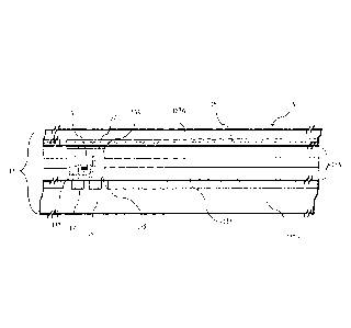
[0050] Please refer to Figures 4A and 4B, showing cross-section views
of a pixel unit structure 1C according to a third preferred embodiment
of the present invention. The pixel unit structure 1C is similar to
the pixel unit structure 1A, both including an active switching
element 13 and a display medium module 15. The pixel unit structure
1C further comprises a carrier board 27.
[0051] Specifically, the carrier board 27 may allow the display medium
module 15 to be disposed thereon, and the active switching element
13 may be disposed on the carrier board 27. The carrier board 27 may
also include a wire, an electrode and other elements for the display
medium module 15 and the active switching element 13 to be electrically
connected to each other. The control signal line 17 and the data signal
line 19 may also be formed on the carrier board 27 and connected to
the active switching element 13.
[0052] Further, the carrier board 27 may include a concave groove 271
(or through hole), wherein may the active switching element 13 be
disposed. The first substrate 157A and/or the second substrate 157B
of the display medium module 15 may also include a through hole 159A,
and the active switching element 13 may be disposed in the concave
groove 271 through the through hole 159A. The carrier board 27 may
14
Date Recue/Date Received 2023-10-26
also include a sidewall insulating layer, an electric conductive pole,
an electric conductive pad, an insulating medium or a combination
thereof, which are disposed in the concave groove 271 for electrically
connecting the active switching element 13 to other elements or
isolating the active switching element 13 from other elements.
[0053] The disposition of the carrier board 27 facilitates the
electrical connection arrangement among the elements of the pixel
unit structure 1C, especially when the pixel unit structure 1C
comprises a plurality of functional elements (not shown in the
drawings).
[0054] Please refer to Figures SA and 5B, showing cross-section views
of a pixel unit structure 1D according to a fourth preferred embodiment
of the present invention. The pixel unit structure 1D is similar to
the pixel unit structure 1A, except that the first substrate 157A
and/or the second substrate 157B of the pixel unit structure 1D
comprises a through hole 159A and/or a concave groove 159B.
[0055]As Figure SA shows, when the active switching element 13 is
disposed in the through hole 159A, its electrode 137 may be exposed
on the first substrate 157A and/or the second substrate 157B. Then
on the electrode 137 may be disposed solder, solder wire, solder bump
and so on for electrically connecting the electrode 137 to other
elements. As Figure 5B shows, when the active switching element 13
is disposed in the concave groove 159B, the active switching element
13 only partially protrudes from the first substrate 157A and/or the
second substrate 157B, and the active switching element 13 may be
electrically connected to the control signal line 17 and the data
signal line 19 in the concave groove 1593.
[WM] The pixel unit structure 1D may also include an optical element
25', which may be formed in the display medium module 15, e.g. formed
on the first electrode 151 or the second electrode 153 (or the optical
element 25' is directly formed from the first electrode 151 or the
Date Recue/Date Received 2023-10-26
second electrode 153), and which may be optically coupled with the
display medium 155. As such, the optical element 25' may guide ambient
light illumination into the display medium module 15, and then the
display medium 155 may modulate the amount or characteristics of the
ambient light illumination leaving the display medium module 15. When
there is sufficient ambient light illumination, the pixel unit
structure 10 may directly use the ambient light illumination to
achieve the function of image pixel display or light modulation. The
optical element 25' may include at least one of a convex lens, a concave
lens and an optical prism.
UMW] Described below are a manufacturing method of a pixel unit
structure according to the present invention and its application as
a display device.
VMS] Please refer to Figure 6, showing a flow diagram of a
manufacturing method of a pixel unit structure according to a fifth
preferred embodiment of the present invention. The manufacturing
method may produce one or a plurality of identical or similar pixel
unit structures lA to 10 of the foregoing preferred embodiments.
Therefore, the technical content of the manufacturing method and the
technical content of the pixel unit structures lA to 10 may be
cross-referenced.
[0059] As Step S101 shows, firstly manufacture an active switching
element; that is, in contrast with a display medium module of a pixel
unit structure, the active switching element is independently
manufactured, rather than being directly manufactured on the display
medium module. The functional elements are also manufactured in
advance and may be manufactured on a same wafer as (or on different
wafers from) the active switching element. The functional elements
and the active switching element may be on the same chip or die (or
different chips or dice)
(0060] Next, as Step S105 shows, assemble the pre-manufactured active
16
DateRecue/DateReceived2023-10-26
switching element to the display medium module. At this moment, the
display medium module may still be in the process of being manufactured;
for example, only after the active switching element is disposed on
the second substrate of the display medium module are the display
medium and the first substrate sequentially disposed on the second
substrate. In addition, in Step 5105, functional elements may also
be simultaneously assembled to the display medium module.
[0061] Further, before performing Step S105, the pre-manufactured
active switching element may be optionally packaged in a package
carrier (e.g. in Step S103); the functional elements may also be
simultaneously packaged in the package carrier. Therefore, if there
is no need of a package carrier, S103 may be omitted.
[0062] Please refer to Figures 7A and 7B, showing a three-dimensional
view and a partial enlargement view of a display device according
to a sixth preferred embodiment of the present invention. The display
device 2 may include a plurality of pixel unit structures lE and a
housing structure 31. The plurality of pixel unit structures lE may
be one of the foregoing pixel unit structures lA to 10 or a technical
combination thereof, and the plurality of pixel unit structures lE
are disposed in the housing structure 31. The housing structure 31
may include a transparent substrate (e.g. a glass or plastic substrate)
for allowing the plurality of pixel unit structures lE to be observed
through the transparent substrate.
[0063]Further, if the display media 155 of the pixel unit structures
lE are made of non-self-luminous medium material, the display device
2 may further include a light source module 33, positioned on any
side of the display medium module 15 of the plurality of pixel unit
structures lE (e.g. rear side, upper side, underside, front side,
left side, right side) for providing light to the display medium module
15. If the display media 155 of the pixel unit structures lE are made
of self-luminous medium material or use ambient light illumination
for its light source, the light source module 33 may be optionally
17
Date Recue/Date Received 2023-10-26
omitted or turned off (i.e. the light source module 33 does not provide
light); or, when the display media 155 made of self-luminous medium
material do not provide sufficient light or when there is insufficient
ambient light illumination, the light source module 33 may provide
additional light.
[1:1064] Further, the pixel unit structure lE may include a functional
element 21 having the function of wireless communication. The
functional element 21 may wirelessly receive the control signals and
data signals from the control module 35 of the display device 2 and
further transmit these signals to the active switching element 13.
That is, the control module 35 may be electrically connected to the
active switching element 13 without passing through a substantial
wire (e.g. the control signal line 17 and the data signal line 19
as shown in Figure 1). The control module 35 may wirelessly control
the active switching element 13 to further control the state of the
display medium 155. In addition, a functional element 21 with the
function of wireless communication may simultaneously be electrically
connected to the active switching elements 13 of a plurality of pixel
unit structures 1E. Therefore, the total number of functional elements
21 may be fewer than the total number of active switching elements
13.
[0065] The foregoing functional element 21 with the function of
wireless communication may be of (but not limited to) the following
types: radio frequency (RF) wireless transmission, Zigbee wireless
transmission, blue-tooth communication, infrared ray, wireless
fidelity (Wi-Fi) wireless transmission, personal area networks (PAN),
local area networks (LAN), near field communication (NFC), radio
frequency identification (RFID), global system for mobile
communication (GSM) and worldwide interoperability for microwave
access (WiMAX), long-term evolution (LTE), 5th generation wireless
communication and one of the combinations thereof.
[0066] Further, the shape combination of the display medium module
18
Date Recue/Date Received 2023-10-26
15 in a pixel unit structure lE may be from (but not limited to) the
following: square, rectangular, fan-shaped, triangular, trapezoid,
round, polygonal, irregular, or one of the combinations thereof. In
the present embodiment, the display medium module 15 is arranged as
a hexagon for an example.
[0067] Further, as Figure 7C shows, the pixel unit structures lE may
be arranged as independently assembled and disassembled, i.e. none
of the elements of any pixel unit structure lE is connected and
integrated to any of the elements of another pixel unit structure
1E. Thus, each of the pixel unit structures lE may be independently
disassembled from the housing structure 31. Therefore, when one of
the pixel unit structures lE is damaged, it may be disassembled and
replaced with a good pixel unit structure 1E.
[0068] Please refer to Figure 8, showing an application schematic view
of the display device 2 of Figure 7A. The display device 2 may not
only be applied to electronic products such as computer and mobile
phone but also to any product that may be equipped with a display
function such as a transportation vehicle, wear products, building
and billboard. Take a car 100 for an example, the display device 2
may serve as a rear car light 101 of the car 100 for showing images
100A of various kinds of driving information (e.g. turning, changing
lanes, slowing down, speeding up, speed per hour, warning and the
like) to other vehicles or pedestrians. In addition, with the
functional element 21 of the pixel unit structure 1E, the display
device 2 may be equipped with the functions of displacement sensing,
hygrothermal sensing, acoustic sensing, electromagnetic sensing,
image capturing and the like for sensing various environmental
information outside the car.
[0069] Besides serving as a rear car light 101 of the car 100, the
display device 2 may also serve as a front car light (not shown in
the drawing), a dashboard (not shown in the drawing) and the like
of the car 100 or may be disposed on the glass of the car 100. In
19
Date Recue/Date Received 2023-10-26
addition, because the display medium module 15 of the plurality of
pixel unit structures lE of the display device 2 may be made of flexible
material, or the plurality of pixel unit structures lE may be
independently assembled and disassembled, the display device 2 may
be disposed along a curved shell 102 of the car 100 to serve as a
lacquer or color painting design on the curved shell 102. This way,
a user may easily change the lacquer or color painting design on the
curved shell 102 and the curved shell 102 may also display images
100A of driving information.
[0070] The display device 2 may also be applied to a traffic notice
board 200 for showing images 200A of destination, route and other
information; the display device 2 may also be applied to a road warning
device 300 for showing an image 300A to inform drivers of the road
conditions ahead. The display device 2 may also serve as a road marker
or road sign and the like.
[0071] The foregoing description illustrates the technical content
of the pixel unit structure, a manufacturing method thereof, and a
display device according to various preferred embodiments of the
present invention. The foregoing description is illustrated of the
present invention rather than limiting of the present invention. Any
change easily made by those ordinarily skilled in the art of the
present invention or any equivalent arrangement falls within the
spirit and scope of the present invention, which is illustrated in
the appended claims.
[0072] Those skilled in the art will readily observe that numerous
modifications and alterations of the device and method may be made
while retaining the teachings of the invention. Accordingly, the above
disclosure should be construed as limited only by the metes and bounds
of the appended claims.
DateRecue/DateReceived2023-10-26