Note: Descriptions are shown in the official language in which they were submitted.
ACTIVE BYPASS CONTROL DEVICE AND METHOD FOR PHOTOVOLTAIC
MODULE
FIELD
[0001] The present disclosure relates to the field of power electronics, in
particular to an
active bypass control device and an active bypass control method for a
photovoltaic module.
BACKGROUND
[0002] In the field of photovoltaic power generation, in order to prevent the
hot spot effect
of a photovoltaic module, a bypass diode is usually arranged in a junction box
of the
photovoltaic module. In a case that a substring in the photovoltaic module is
shaded and the
power thereof is insufficient, the current is automatically transferred from
the substring to the
external parallel diode loop, avoiding heat generation of the abnormal
substring as a load,
while not affecting the power generation of other substrings. In some module-
level products,
such as a shutdown device and an optimizer, a diode is also connected in
parallel with the
output port of the photovoltaic module. In the case of device abnormal
shutdown, the branch
in which the photovoltaic module is located is bypassed, so that the remaining
photovoltaic
modules in the same substring are not affected.
[0003] The current of a conventional photovoltaic module is generally about
10A, and the
current of a double-sided photovoltaic module even reaches 13A. When entering
the bypass
mode, the current flows through the parallel diode. Depending on the
performance of the
diode, the loss usually ranges from 3W to 6W. The large power consumption
results in the
temperature in the conventional junction box being above 150 . The junction
box may heat up
and bulge under the continuous high temperature. In this case, the life of the
diode is reduced,
resulting in reduced reliability of the product. Further, in order to improve
heat dissipation, a
metal piece having a larger area may be required for the diode, or a potting
sealant with better
thermal conductivity may be used, or a diode with better performance may be
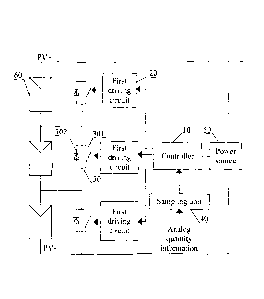
selected, which
all result in increase of the cost. In addition, the system loss is large,
bringing a certain loss to
the system power generation.
1
13346669.3 - -
34273/47
CA 3049551 2019-07-15
SUMMARY
[0004] There are provided an active bypass control device and an active bypass
control
method for a photovoltaic module in the present disclosure, to solve problems
in the
conventional technology of low reliability, high cost and large system loss.
[0005] The following technical solutions are provided in the present
disclosure.
[0006] In a first aspect, an active bypass control device for a photovoltaic
module is
provided. The active bypass control device includes a power source, a sampling
unit, a
controller, N first driving circuits, and N first controllable switches, where
N is a positive
integer, where
[0007] an output end of the power source is connected to a power supply end of
the
controller;
[0008] an output end of the sampling unit is connected to an input end of the
controller;
[0009] each of the N first controllable switches is connected between one of N
pairs of
bypass ports corresponding to the first controllable switch, and the first
controllable switch
includes a first switch and a first diode that are antiparallel, the first
diode is reversely
connected between the pair of bypass ports, and a control end of the first
switch is connected
to one output end of the controller via one of the N first driving circuits
corresponding to the
first controllable switch;
[0010] the sampling unit is configured to: detect, for each first controllable
switch, analog
quantity information of the first controllable switch, and output a sampling
signal based on the
analog quantity information; and
[0011] the controller is configured to: determine, based on the sampling
signal, whether the
analog quantity information of the first controllable switch meets a
predetermined bypass
condition; and control, in a case that the analog quantity information meets
the predetermined
bypass condition, the first switch in the first controllable switch to be
turned on by using the
first driving circuit corresponding to the first controllable switch.
[0012] In an embodiment, the controller is further configured to: after
controlling the first
switch in the first controllable switch to be turned on,
control the first switch to be turned off by using the first driving circuit
corresponding to
-2-
13346669.3
34273/47
CA 3049551 2019-07-15
the first controllable switch in a case that a time period during which the
first switch is turned
on exceeds a first preset time period; and
determine, based on a sampling signal outputted by the sampling unit after
performing
re-detecting on the first controllable switch, whether the analog quantity
information
corresponding to the sampling signal meets the predetermined bypass condition
[0013] In an embodiment, the controller is further configured to: before
determining
whether the analog quantity information meets the predetermined bypass
condition,
perform software filtering on the sampling signal.
[0014] In an embodiment, the analog quantity information is one of a voltage,
a current,
power, and a branch temperature;
[0015] in a case that the analog quantity information is the voltage, the
predetermined
bypass condition is that, the number of times that a voltage of the first
controllable switch is
lower than a preset voltage threshold is greater than or equal to a preset
number of times, or a
time period during which the voltage of the first controllable switch is lower
than the preset
voltage threshold is greater than or equal to a second preset time period;
[0016] in a case that the analog quantity information is the current, the
predetermined
bypass condition is that, the number of times that a current of the first
controllable switch is
greater than a preset current threshold is greater than or equal to a preset
number of times, or a
time period during which the current of the first controllable switch is
greater than the preset
current threshold is greater than or equal to a second preset time period;
[0017] in a case that the analog quantity information is the power, the
predetermined bypass
condition is that, the number of times that power of the first controllable
switch is greater than
a preset power threshold is greater than or equal to a preset number of times,
or a time period
during which the power of the first controllable switch is greater than the
preset power
threshold is greater than or equal to a second preset time period; and
[0018] in a case that the analog quantity information is the branch
temperature, the
predetermined bypass condition is that, the number of times that a branch
temperature of the
first controllable switch is higher than a preset temperature threshold is
greater than or equal
to a preset number of times, or a time period during which the branch
temperature of the first
-3-
13346669.3
34273/47
CA 3049551 2019-07-15
controllable switch is greater than the preset temperature threshold is
greater than or equal to a
second preset time period.
[0019] In an embodiment, the first controllable switch is a triode having a
body diode or a
switch transistor having a body diode; and
[0020] the first switch is a relay, a triode or a switch transistor.
[0021] In an embodiment, an input end of the power source is connected between
two ends
of the photovoltaic module.
[0022] In an embodiment, the N pairs of bypass ports are arranged between two
ends of the
photovoltaic module, or the N pairs of bypass ports are arranged between two
ends of at least
one substring in the photovoltaic module, or the N pairs of bypass ports are
arranged between
two ends of the photovoltaic module and two ends of at least one substring in
the photovoltaic
module.
[0023] In an embodiment, in a case that the N pairs of bypass ports are
arranged between
the two ends of the photovoltaic module and the active bypass control device
for a
photovoltaic module is applied to a shutdown device, the other output end of
the controller is
connected to a control end of a second controllable switch in the shutdown
device via a
second driving circuit;
[0024] the second controllable switch is connected between the first
controllable switch and
the photovoltaic module; and
[0025] the controller is further configured to:
control the second controllable switch to be turned on by using the second
driving circuit
in a case that the photovoltaic module is in a normal condition; and
control the second controllable switch to be turned off by using the second
driving circuit
in a case that the photovoltaic module is in an abnormal condition.
[0026] In a second aspect, there is provided an active bypass control method
for a
photovoltaic module, applied to the active bypass control device for a
photovoltaic module
described in the first aspect. The active bypass control method includes:
[0027] detecting, by the sampling unit for each first controllable switch,
analog quantity
-4-
13346669.3
34273/47
CA 3049551 2019-07-15
information of the first controllable switch, and outputting, by the sampling
unit, a sampling
signal based on the analog quantity information;
[0028] determining, by the controller based on the sampling signal, whether
the analog
quantity information of the first controllable switch meets a predetermined
bypass condition;
and
[0029] controlling, by the controller, the first switch in the first
controllable switch to be
turned on by using the first driving circuit corresponding to the first
controllable switch in a
case that the analog quantity information meets the predetermined bypass
condition.
[0030] In an embodiment, after controlling the first switch in the first
controllable switch to
be turned on, the active bypass control method further includes:
[0031] counting, by the controller, a time period during which the first
switch is turned on;
[0032] determining, by the controller, whether the time period during which
the first switch
is turned on exceeds a first preset time period;
[0033] controlling, by the controller, the first switch to be turned off by
using the
corresponding first driving circuit in a case that the time period during
which the first switch
is turned on exceeds the first preset time period; and
[0034] re-detecting, by the sampling unit, analog quantity information of the
first
controllable switch, and re-outputting, by the sampling unit, a sampling
signal based on the
analog quantity information.
[0035] With the active bypass control device for a photovoltaic module
provided in the
present disclosure, in the case that the controller determines, based on the
sampling signal
outputted by the sampling unit, that the analog quantity information of the
first controllable
switch meets the predetermined bypass condition, the controller controls the
first switch in the
first controllable switch to be turned on by using the first driving circuit
corresponding to the
first controllable switch, so that the first diode in the first controllable
switch is prevented
from having a large power consumption, thereby solving the problems in the
conventional
technology of low reliability, high cost and large system loss caused by the
large power
consumption of the first diode.
-5-
13346669.3
34273/47
CA 3049551 2019-07-15
BRIEF DESCRIPTION OF THE DRAWINGS
[0036] In order to more clearly illustrate technical solutions in embodiments
of the present
disclosure or in the conventional technology, the drawings used in the
description of the
embodiments or the conventional technology are briefly described below.
Apparently, the
drawings in the following description show only some embodiments of the
present disclosure,
and other drawings may be obtained by those skilled in the art from the
drawings without any
creative work.
[0037] Figure 1 is a schematic diagram showing an active bypass control device
for a
photovoltaic module according to an embodiment of the present disclosure;
[0038] Figure 2 is a schematic diagram showing an active bypass control device
for a
photovoltaic module according to another embodiment of the present disclosure;
[0039] Figure 3 is a schematic diagram showing an active bypass control device
for a
photovoltaic module according to another embodiment of the present disclosure;
[0040] Figure 4 is a schematic diagram showing an active bypass control device
for a
photovoltaic module according to another embodiment of the present disclosure;
[0041] Figure 5 is a schematic diagram showing an active bypass control device
for a
photovoltaic module according to another embodiment of the present disclosure;
[0042] Figure 6 is a flowchart showing an active bypass control method for a
photovoltaic
module according to an embodiment of the present disclosure; and
[0043] Figure 7 is a flowchart showing an active bypass control method for a
photovoltaic
module according to another embodiment of the present disclosure.
DETAILED DESCRIPTION OF EMBODIMENTS
[0044] Technical solutions of embodiments of the present disclosure are
clearly and
completely described in the following in conjunction with the drawings of the
embodiments
of the present disclosure. Apparently, the embodiments described in the
following are only
some embodiments of the present disclosure, rather than all the embodiments.
Any other
embodiments obtained by those skilled in the art based on the embodiments in
the present
disclosure without any creative work fall in the scope of protection of the
present disclosure.
-6-
13346669.3
34273/47
CA 3049551 2019-07-15
[0045] Reference is made to Figure 1, which is a schematic diagram showing an
active
bypass control device for a photovoltaic module according to an embodiment of
the present
disclosure. In this embodiment, the active bypass control device may include:
a power source
50, a sampling unit 40, a controller 10, N first driving circuits 20, and N
first controllable
switches 30, where N is a positive integer.
[0046] An output end of the power source 50 is connected to a power supply end
of the
controller 10, so that the power source 50 supplies power required for
operation of the
controller 10. The power source 50 may also supply power required for
operation of other
modules in the device. In an embodiment, an input end of the power source 50
is connected to
the photovoltaic module to take power from the photovoltaic module side. In
this case, circuit
configuration of the device is simplified, facilitating maintenance and
overhaul of the device.
Alternatively, the power source 50 is implemented by an independent external
power source
and is not connected to an output line of the photovoltaic module, which can
improve
reliability of the device provided in the present disclosure to some extent.
In this case, the
normal operation of the power source 50 can not be affected by partial failure
of the output
line of the photovoltaic module, and thus normal power consumption of the
controller 10 and
other modules connected with the power source 50 can not be affected. It
should be noted that
the power source 50 is not limited to those described in the embodiment of the
present
disclosure, as long as the power source 50 can supply the power to the
controller 10 and the
other modules.
[0047] The N first controllable switches 30 are respectively connected between
N pairs of
bypass ports. In a case that a bypass device is required only for the
photovoltaic module, the
N pairs of bypass ports are arranged between two ends of the photovoltaic
module, and in this
case N=1. In a case that a bypass device is required for each of N substrings
in the
photovoltaic module, each of the N pairs of bypass ports is arranged between
two ends of one
of the N substrings in the photovoltaic module, and in this case N>1. In a
case that a bypass
device is required for the photovoltaic module and a bypass device is required
for each of
(N-1) substrings among the N substrings in the photovoltaic module, one of the
N pairs of
bypass ports is arranged between the two ends of the photovoltaic module, and
each of the
remaining (N-1) pairs among the N pairs of bypass ports is arranged between
two ends of one
of the (N-1) substrings, and in this case N>2. It should be noted that the
above shows
- 7 -
I 3346669.3
34273/47
CA 3049551 2019-07-15
preferred solutions. In practical applications, the N pairs of bypass ports
may be arranged for
one or some substrings in the photovoltaic module, each of which is provided
with the first
controllable switch connected in parallel with the substring, while each of
other substrings
than the one or some substrings is only provided with an antiparallel diode.
The setting of the
N pairs of bypass ports is not limited thereto, which may depend on
application environments.
[0048] Figure 1 shows a case that the photovoltaic module includes three
substrings 60,
each of which is provided with a first driving circuit 20 and a first
controllable switch 30. The
following description is given by taking the case shown in Figure 1 as an
example.
[0049] Each substring 60 corresponds to one first controllable switch 30, and
each first
controllable switch 30 corresponds to one first driving circuit 20. Each first
controllable
switch 30 is driven by the corresponding first driving circuit 20 under
control of the controller
10, to bypass the substring 60 connected in parallel with the first
controllable switch 30, so as
to achieve independent protection for the substring 60.
[0050] The first controllable switch 30 includes a first switch 301 and a
first diode 302. The
first diode 302 is connected in antiparallel with the corresponding substring
60, and the first
switch 301 is connected in parallel with the corresponding substring 60. A
control end of the
first switch 301 is connected to one output end of the controller 10 via the
corresponding first
driving circuit 20, so that the first switch 301 receives a control signal
transmitted by the
controller 10 via the corresponding first driving circuit 20. The first switch
301 is turned on or
turned off based on the received control signal. The first switch 301 may be
implemented by a
relay, a triode or a switch transistor. The first diode 302 may be implemented
by a bypass
diode provided in the photovoltaic module, or may be implemented by a diode
installed
together with the first switch 301. The first controllable switch 30 may be
implemented by a
triode having a body diode or a switch transistor having a body diode. The
implementations of
the above components are not limited thereto, which may depend on the
application
environments.
[0051] The sampling unit 40 is configured to: detect, for each first
controllable switch 30,
analog quantity information of the first controllable switch 30. An output end
of the sampling
unit 40 is connected to an input end of the controller 10 .The sampling unit
40 generates a
sampling signal based on the analog quantity information and provides the
sampling signal to
-8-
133466693
34273/47
CA 3049551 2019-07-15
the controller 10. The analog quantity information of the first controllable
switch 30 that may
be acquired by the sampling unit 40 is one of a voltage, a current, power, and
a branch
temperature, which is not limited herein and may be depend on the application
environments.
[0052] The controller 10 operates on power supplied by the power source 50,
and
determines, based on the sampling signal provided by the sampling unit 40,
whether the
analog quantity information of the first controllable switch 30 meets a
predetermined bypass
condition. If it is determined that the analog quantity information of the
first controllable
switch 30 meets the predetermined bypass condition, the controller 10 controls
the first switch
301 in the first controllable switch 30 to be turned on by using the
corresponding first driving
circuit 20. Since an internal resistance of the first switch 301 is smaller
than that of the first
diode 302, a current generated by the corresponding substring 60 is mainly or
completely
transmitted through the first switch 301 in the conductive state, so that
power consumption of
the first diode 302 in the first controllable switch 30 in the conductive
state is reduced.
[0053] With the active bypass control device for a photovoltaic module
according this
embodiment, the first diode in the first controllable switch is prevented from
having a large
power consumption due to a large current, thereby solving problems in the
conventional
technology of low reliability, high cost and large system loss caused by the
large power
consumption of the first diode.
[0054] It should be noted that, in actual applications, if the first switch in
the first
controllable switch corresponding to a shaded photovoltaic power generation
unit is kept in
the conductive state, an output end of the photovoltaic power generation unit
is kept in the
short-circuited state, and the outputted current is transmitted through the
first switch. In this
case, even if the shaded photovoltaic power generation unit is no longer
unshaded to restore to
a normal operation state, the photovoltaic power generation unit can not
provide power
abnormally, which is apparently unreasonable.
[0055] Based on the above embodiment, an active bypass control device of a
photovoltaic
module is further provided according to another embodiment of the present
disclosure. In this
embodiment, after controlling the first switch to be turned on by the
corresponding first
driving circuit, the controller counts a time period during which the first
switch is turned on.
When the time period during which the first switch is turned on exceeds a
first preset time
-9-
13346669.3
34273/47
CA 3049551 2019-07-15
period, the controller transmits a control signal to the corresponding first
driving circuit, to
control the corresponding first switch to be turned off by using the first
driving circuit, so that
the corresponding photovoltaic power generation unit is no longer forward
short-circuited by
the first switch.
[0056] The controller re-receives the sampling signal of the photovoltaic
power generation
unit provided by the sampling unit, and determines whether the analog quantity
information of
the corresponding first controllable switch meets the predetermined bypass
condition. If the
photovoltaic power generation unit is no longer unshaded, the photovoltaic
power generation
unit may be re-connected to a power supply network for normal operation. If
the photovoltaic
power generation unit is still shaded and can not operate normally, the
controller controls the
corresponding first switch to be turned on again based on the sampling signal
provided by the
sampling unit, so that the current of the photovoltaic power generation unit
is transmitted
through the first switch. The controller performs the counting again, and the
above process is
repeatedly performed until the photovoltaic power generation unit is no longer
unshaded.
Then, the controller controls the first switch to be turned off, so that the
output end of the
photovoltaic power generation unit is no longer short-circuited. The
photovoltaic power
generation unit is connected to the power supply network for the normal
operation.
[0057] Other structures and operation principles in this embodiment are the
same as those in
the above embodiments, which are not repeated herein.
[0058] Based on the above embodiments, the sampling process and the
determination
process are described in detail below.
[0059] In an embodiment, after receiving the sampling signal, the controller
10 may further
perform software filtering on the received sampling signal to filter out
electromagnetic
interference to the sampling signal during transmission, so as to improve the
accuracy of the
controller 10 in determining whether the analog quantity information of the
first controllable
switch 30 meets the predetermined bypass condition, and thus the controller 10
transmits the
control signal to the corresponding first driving circuit 20 in time and
accurately.
[0060] The first controllable switch may have different circuit structures due
to different
analog quantity information acquired by the sampling unit, and the
predetermined bypass
condition may also vary with the analog quantity information.
- 10 -
13346669.3
34273/47
CA 3049551 2019-07-15
[0061] Reference is made to Figure 2, which is schematic diagram showing an
active
bypass control device for a photovoltaic module according to another
embodiment of the
present disclosure. The first controllable switch 30 is implemented by a
switch transistor
having a body diode, and other structures in this embodiment are the same as
the embodiment
shown in Figure I, which are not repeated herein.
[0062] The body diode in the first controllable switch 30 is connected in
antiparallel with
the corresponding substring 60, and a component realizing the switch function
in the first
controllable switch 30 is connected in parallel with the substring 60. The
sampling unit 40
acquires a voltage of the first controllable switch 30. The sampling unit 40
may directly
acquire voltages of the first controllable switches 30. Alternatively, the
sampling unit 40 may
acquire voltages at nodes, and obtains the voltages of the first controllable
switches 30 by
subtraction between adjacent nodes.
[0063] In a case that the sampling unit acquires the voltage of the first
controllable switch,
the predetermined bypass condition is that, the number of times that the
voltage of the first
controllable switch is lower than a preset voltage threshold is greater than
or equal to a preset
number of times, or a time period during which the voltage of the first
controllable switch is
lower than the preset voltage threshold is greater than or equal to a second
preset time period.
[0064] Reference is made to Figure 3, which is schematic diagram showing an
active
bypass control device for a photovoltaic module according to another
embodiment of the
present disclosure. Based on the embodiment shown in Figure 2, a sampling
resistor 303 is
connected in series in a loop of the first controllable switch 30, and is used
to acquire a current
of the corresponding first controllable switch 30. In an embodiment, the
current of the first
controllable switches 30 may be acquired by a current sensor. The sampling
resistor 303 or the
current sensor may be arranged between the first controllable switch 30 and a
positive
terminal or a negative terminal of the substring 60. In this case, a correct
current may be
obtained.
[0065] In a case that the sampling unit acquires the current of the first
controllable switch,
the predetermined bypass condition is that, the number of times that the
current of the first
controllable switch is greater than a preset current threshold is greater than
or equal to a preset
number of times, or a time period during which the current of the first
controllable switch is
-11-
13346669.3
34273/47
CA 3049551 2019-07-15
greater than a preset current threshold is greater than or equal to a second
preset time period.
[0066] Further, the analog quantity information of the first controllable
switch may also be
the power or the branch temperature. In a case that the analog quantity
information is the
power, the predetermined bypass condition is that, the number of times that
the power of the
first controllable switch is greater than a preset power threshold is greater
than or equal to a
preset number of times, or a time period during which the power of the first
controllable
switch is greater than the preset power threshold is greater than or equal to
a second preset
time period. In a case that the analog quantity information is the branch
temperature, the
predetermined bypass condition is that, the number of times that the branch
temperature of the
first controllable switch is higher than a preset temperature threshold is
greater than or equal
to a preset number of times, or a time period during which the branch
temperature of the first
controllable switch is greater than the preset temperature threshold is
greater than or equal to a
second preset time period.
[0067] It should be noted that the preset number of times and the second
preset time period
are set in order to avoid a detection error and improve detection accuracy, so
that a
determination result of the controller is reliable. The preset number of times
and the second
preset time period may be set according to the application environments, which
are not limited
herein. Further, the analog quantity information of the first controllable
switch is not limited
to those described in the embodiments of the present disclosure, as long as
the analog quantity
information can indicate a physical state of the first controllable switch.
[0068] Reference is made to Figure 4, which is a schematic diagram showing an
active
bypass control device for a photovoltaic module according to another
embodiment of the
present disclosure. It can be seen from Figure 4 that, the first switch 301 in
the first
controllable switch 30 is implemented by a relay. The first driving circuit 20
transmits a drive
current to a coil of the relay based on the control signal of the controller
10, so that the coil of
the relay is energized. After the coil of the relay is energized, a normally
open contact of the
relay is controlled to be closed. The output current of the corresponding
substring 60 may be
transmitted through the contact of the relay, so that the power consumption of
the first diode
302 can be reduced.
[0069] In the embodiment shown in Figure 4, the analog quantity information of
the first
- 12 -
13346669 3
34273/47
CA 3049551 2019-07-15
controllable switch 30 may also be acquired by the sampling unit, which is not
repeated
herein.
[0070] Other structures and operation principles in this embodiment are the
same as those in
the above embodiments, which are not repeated herein.
[0071] The active bypass control device according to any one above embodiment
may be
used separately or integrated in a shutdown device or an optimizer of the
photovoltaic module.
Reference is made to Figure 5, which is a schematic diagram showing a shutdown
device of a
photovoltaic module according to an embodiment of the present disclosure. In
this
embodiment, N=1, the photovoltaic power generation unit is implemented as a
photovoltaic
module. Based on any of the above embodiments, the active bypass control
device further
includes a second driving circuit 70 and a second controllable switch 80. The
first controllable
switch 30 and the photovoltaic module 60 are indirectly connected in parallel
with each other
via the second controllable switch 80. That is, the second controllable switch
80 is connected
between the first controllable switch 30 and the photovoltaic module 60, and a
control end of
the second controllable switch 80 is connected to the other output end of the
controller 10 via
the second driving circuit 70.
[0072] In this embodiment, for the photovoltaic module 60, only one of the
first
controllable switch 30 and the second controllable switch 80 is turned on at
any time instant.
In a case that the photovoltaic module 60 is in a normal condition, the
controller 10 controls
the second controllable switch 80 to be turned on by using the second driving
circuit 70, to
connect the photovoltaic module 60 to the power supply network. In a case that
the
photovoltaic module 60 is in an abnormal condition, the controller 10 controls
the second
controllable switch 80 to be turned off by using the second driving circuit 70
to disconnect the
photovoltaic module 60 from the power supply network.
[0073] With the technical solutions according to the embodiment of the present
disclosure, a
shaded photovoltaic module can be removed from the power supply network, and
the
outputted electric energy of the shaded photovoltaic module can be controlled
to ensure the
normal operation of unshaded photovoltaic modules, thereby improving the
reliability of the
power supply network.
[0074] Other structures and operation principles in this embodiment are the
same as those in
-13-
13346669.3
34273/47
CA 3049551 2019-07-15
the above embodiments, which are not repeated herein.
[0075] An active bypass control method for a photovoltaic module is further
provided
according to an embodiment of the present disclosure.
[0076] Reference is made to Figure 6, which is a flowchart showing an active
bypass
control method for a photovoltaic module according to an embodiment of the
present
disclosure. The active bypass control method is applied to a control module in
the active
bypass control device for a photovoltaic module. As shown in Figure 6, the
active bypass
control method may include the following steps S100 to S130.
[0077] In step S100, a sampling unit detects analog quantity information of a
first
controllable switch, and outputs a sampling signal based on the analog
quantity information.
[0078] The sampling unit detects the analog quantity information of the first
controllable
switch corresponding to the photovoltaic power generation unit, and outputs
the sampling
signal generated based on the analog quantity information to a controller. The
analog quantity
information may be one of a voltage, a current, power, and a branch
temperature.
[0079] In step S110, a controller determines, based on the sampling signal,
whether the
analog quantity information meets a predetermined bypass condition. If the
analog quantity
information meets the predetermined bypass condition, the method proceeds to
step S120. If
the analog quantity information does not meet the predetermined bypass
condition, the
method proceeds to step S130.
[0080] The controller determines, based on the sampling signal provided by the
sampling
unit, whether the analog quantity information of the first controllable switch
corresponding to
the sampling signal meets the predetermined bypass condition. If the
predetermined bypass
condition is met, step S120 is performed. If the predetermined bypass
condition is not met,
step S130 is performed.
[0081] In step S120, the controller controls a first switch in the first
controllable switch to
be turned on by using a first driving circuit corresponding to the first
controllable switch.
[0082] In a case that the analog quantity information of the first
controllable switch meets
the predetermined bypass condition, the controller outputs a control signal to
the
corresponding first driving circuit, and controls the first switch in the
first controllable switch
-14-
13346669 3
34273/47
CA 3049551 2019-07-15
to be turned on by using the first driving circuit, so that the current
generated by the shaded
photovoltaic power generation unit is transmitted through the first switch,
thereby preventing
the first diode in the first controllable switch from having a large power
consumption due to a
large current.
[0083] In step S130, the controller continues to receive the sampling signal.
[0084] In a case that the analog quantity information of the first
controllable switch does not
meet the predetermined bypass condition, the controller continues to receive
the sampling
signal provided by the sampling unit.
[0085] With the active bypass control method for a photovoltaic module
according to this
embodiment, the controller reads the sampling signal provided by the sampling
unit, which
may reflect the state of the first controllable switch. If the controller
determines, based on the
sampling signal, that the first diode in the first controllable switch is in
the conductive state,
the controller transmits a control signal to the corresponding first driving
circuit, to control the
first switch to be turned on by using the first driving circuit. Since an
internal resistance of the
first switch is smaller than that of the first diode, the current generated by
the shaded
photovoltaic power generation unit is transmitted through the first switch in
the conductive
state, so that the first diode in the first controllable switch is prevented
from having a large
power consumption, thereby solving problems in the conventional technology of
low
reliability, high cost and large system loss caused by the large power
consumption of the first
diode.
[0086] Reference is made to Figure 7, which is a flowchart showing an active
bypass
control method for a photovoltaic module according to another embodiment of
the present
disclosure. Based on the active bypass control method for a photovoltaic
module shown in
Figure 6, the active bypass control method shown in Figure 7 may further
include the
following steps S200 to S220.
[0087] In step S200, the controller counts a time period during which the
first switch is
turned on.
[0088] Upon issue of the control command for controlling the first switch to
be turned on,
the controller counts the time period during which the first switch is turned
on, i.e., counts a
time period during which the first switch is in the conductive state.
- 15 -
13346669 3
34273/47
CA 3049551 2019-07-15
[0089] In step S210, the controller determines whether the time period during
which the
first switch is turned on exceeds a first preset time period. If the time
period during which the
first switch is turned on exceeds the first preset time period, the method
proceeds to step
S220.
[0090] In a case that the controller determines that the time period during
which the first
switch is turned on exceeds the first preset time period, step S220 is
performed.
[0091] In step S220, the controller controls the first switch to be turned off
by using the
corresponding first driving circuit.
[0092] In the case that the controller determines that the time period during
which the first
switch is turned on exceeds the first preset time period, the controller
transmits a control
command to the corresponding first driving circuit again to control the first
switch to be
turned off. In this case, the current generated by the corresponding
photovoltaic power
generation unit is no longer transmitted through the first switch.
[0093] After step S220 is performed, step S100 is repeated.
[0094] After the controller controls the first switch to be turned off, the
controller re-reads
the sampling signal provided by the sampling unit, and outputs a control
signal based on the
obtained sampling signal.
[0095] With the active bypass control method for a photovoltaic module
according to this
embodiment, the controller counts the time period during which the first
switch is in the
conductive state. In the case that the time period during which the first
switch is in the
conductive state exceeds the first preset time period, the controller controls
the first switch to
be turned off, and step S100 is performed again to continue monitoring the
analog quantity
information of the first controllable switch. In the active bypass control
method according to
this embodiment, by cyclically controlling the first switch to be turned on or
off, the first
switch is prevented from being kept in the conductive state after being turned
on once, thereby
avoiding that the shaded photovoltaic power generation unit, after being
unshaded, can not be
reconnected to the power supply network for the normal operation. In this way,
the power
consumption of the first diode in the first controllable switch can be
reduced, and the shaded
photovoltaic power generation unit, after being unshaded, can be reconnected
to the power
supply network in time, thereby improving the utilization rate of the
photovoltaic power
-16-
13346669 3
34273/47
CA 3049551 2019-07-15
generation unit.
[0096] In an embodiment, corresponding to the active bypass control device for
a
photovoltaic module shown in Figure 5, the active bypass control method for a
photovoltaic
module shown in Figure 6 or Figure 7 may further include the following
processes before step
S100 is performed.
[0097] In a case that the photovoltaic module is in a normal condition, the
controller
controls a second controllable switch to be turned on by using a corresponding
second driving
circuit.
[0098] In a case that the photovoltaic module is in an abnormal condition, the
controller
controls the second controllable switch to be turned off by using the
corresponding second
driving circuit.
[0099] With the active bypass control method for a photovoltaic power
generation unit
according to this embodiment, a shaded photovoltaic module can be removed from
the power
supply network, and the outputted electric energy of the shaded photovoltaic
module can be
controlled to ensure the normal operation of unshaded photovoltaic modules,
thereby
improving the reliability of the power supply network. Other operation
principles in this
embodiment are the same as those in the above embodiments, which are not
repeated herein.
[0100] Embodiments of the present disclosure are described in a progressive
manner, each of
the embodiments emphasizes differences from other embodiments, and the same or
similar
parts among the embodiments can be referred to each other. For the device
disclosed in the
embodiments, since the device corresponds to the method disclosed in the
embodiments, the
description is relatively simple, and the related parts can be referred to the
description of the
method.
[0101] The foregoing embodiments are only preferred embodiments of the present
disclosure and are not meant to limit the present disclosure. The preferred
embodiments
according to the present disclosure are disclosed above, and are not intended
to limit the
present disclosure. Those skilled in the art may make, based on the disclosed
method and
technical content, some variations and improvements on the technical solutions
of the present
disclosure, or make some equivalent variations on the embodiments without
departing from
.. the scope of the technical solutions. All simple modifications, equivalent
variations and
- 17 -
13346669.3
34273/47
CA 3049551 2019-07-15
improvements made based on the technical essence fall in the scope of the
technical solutions
of the present disclosure.
-18-
13346669.3
34273/47
CA 3049551 2019-07-15