Note: Descriptions are shown in the official language in which they were submitted.
- 1 -
THIN FILM SUBSTRATES INCLUDING CROSSLINKED CARBON
NANOSTRUCTURES AND RELATED METHODS
TECHNICAL FIELD
Embodiments of the disclosure relate generally to thin film substrates for use
in
Surface Enhanced Raman Spectroscopy (SERS), filtration, and chemical sensing,
and to
methods of making and using the thin film substrates. More particularly,
embodiments of the
disclosure relate to thin film substrates including crosslinked carbon
nanostructures and to
methods of making and using the thin film substrates.
BACKGROUND
Surface Enhanced Raman Spectroscopy (SERS) is an analytical technique used to
detect a SERS-active analyte, such as a biological molecule. In SERS, a liquid
sample to be
analyzed is placed on a SERS substrate and up to a single molecule of the
analyte is
detectable. Conventional SERS substrates include metallic nanoparticles on a
solid support,
such as borosilicate glass or mica. The SERS substrate may also be a carbon
nanotube (CNT)
mat, which is conventionally formed using mechanical compression, physical
compression, or
destructive electron beam irradiation techniques. Since these techniques use
compression or
laser ablation, the techniques may be destructive to the SERS substrate. The
mechanical
compression of CNTs into mats relies on weak van der Waals interactions
between the CNTs,
while the laser ablation requires high energy electron beams to fuse the CNTs
together, which
often results in excessive destruction of the sp2 bonding and can adversely
affect CNT
properties. Due to the weak van der Waals interactions between the CNTs,
mechanically
compressed CNTs may absorb liquid and swell when exposed to liquid samples.
Moreover,
conventional methods are not industrially viable as they often utilize
specialized equipment,
such as high energy lasers or high pressure/high temperature (HPHT) reaction
chambers.
DISCLOSURE
Embodiments disclosed herein include methods of making a thin film substrate.
The
method comprises exposing carbon nanostructures to a crosslinker to crosslink
the carbon
nanostructures. The crosslinked carbon nanostructures are recovered and
disposed on a
support substrate.
Date Recue/Date Received 2020-12-11
- 2 -
In additional embodiments, there is provided a method of making a thin film
substrate,
comprising: forming a solution of carbon nanostructures; reacting the carbon
nanostructures
with a crosslinker to form a suspension comprising crosslinked carbon
nanostructures
comprising covalent bonds between the crosslinked carbon nanostructures and
the crosslinker,
the crosslinker comprising a multivalent cation source compound comprising an
oligothiophene, an oligoaniline, phenylene sulfide, pyrrole, urethane, a
metallic oxide, boron
oxide, acetoxysilane, or a combination thereof; filtering the crosslinked
carbon nanostructures
from the suspension; and disposing the crosslinked carbon nanostructures on a
support
substrate.
In additional embodiments, thin film substrates are disclosed. The thin film
substrate
comprises crosslinked carbon nanostructures on a support substrate. The
crosslinked carbon
nanostructures comprise a crosslinker between the carbon nanostructures.
In yet additional embodiments, methods of performing surface enhanced Raman
spectroscopy (SERS) to detect a SERS-active analyte are disclosed. The method
comprises
providing a SERS-active analyte on a thin film substrate, exposing the thin
film substrate to
Raman scattering, and detecting the SERS-active analyte. The thin film
substrate comprises
crosslinked carbon nanostructures on a support substrate and the crosslinked
carbon
nanostructures comprise a crosslinker between the carbon nanostructures.
Date Recue/Date Received 2020-12-11
- 2a -
BRIEF DESCRIPTION OF THE DRAWINGS
FIG. 1 is a schematic diagram of a thin film substrate including the
crosslinked carbon
nanotubes on a support substrate according to an embodiment of the disclosure;
FIG. 2 is a schematic diagram of a thin film substrate including crosslinked
carbon
nanotubes according to an embodiment of the disclosure;
FIGs. 3a and 3b are schematic diagrams of thin film substrates including
crosslinked
carbon nanotubes according to another embodiment of the disclosure;
FIG. 4 is a schematic diagram of a thin film substrate including crosslinked
carbon
nanotubes according to yet another embodiment of the disclosure;
FIG. 5 is a schematic diagram of a thin film substrate including crosslinked
carbon
nanotubes according to yet another embodiment of the disclosure;
FIG. 6 is a schematic diagram of a thin film substrate including crosslinked
carbon
nanotubes according to an additional embodiment of the disclosure;
FIG. 7 is a photograph of crosslinked carbon nanotubes according to an
additional
embodiment of the disclosure;
FIG. 8 is a fourier transform infrared (FTIR) spectrum of the crosslinked
carbon
nanotubes shown in FIG. 7.
Date Recue/Date Received 2020-12-11
CA 03049659 2019-07-08
WO 2018/132558 PCT/US2018/013300
- 3 -
MODE(S) FOR CARRYING OUT THE INVENTION
Illustrations presented herein are not meant to be actual views of any
particular
material or component, but are merely idealized representations that are
employed to
describe embodiments of the disclosure.
The following description provides specific details, such as material types,
compositions, material thicknesses, and processing conditions in order to
provide a thorough
description of embodiments of the disclosure. However, a person of ordinary
skill in the art
will understand that the embodiments of the disclosure may be practiced
without employing
these specific details. Indeed, the embodiments of the disclosure may be
practiced in
conjunction with conventional techniques employed in the industry. In
addition, the
description provided below does not form a complete process flow for forming a
thin film
substrate. Only those process acts and structures necessary to understand the
embodiments of
the disclosure are described in detail below. Additional acts or materials to
form the thin film
substrates may be performed by conventional techniques.
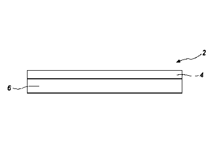
A thin film substrate 2 is formed from and includes crosslinked carbon
nanostructures
4 on a support substrate 6, as shown in FIG. 1. The thin film substrate 2 may
be used for
Surface Enhanced Raman Spectroscopy (SERS), filtration, or chemical sensing.
The carbon
nanostructures may be exposed to a crosslinker, such as in solution, to
crosslink the carbon
nanostructures. As described in more detail below, the carbon nanostructures
and crosslinker
may be combined in an appropriate solvent, such as water, an organic solvent,
or
combinations thereof The crosslinked carbon nanostructures 4 may be configured
as carbon
nanostructure mats or in other configurations. As used herein, the term
"carbon nanostructure
mat" means and includes a sheet of carbon nanostructures. The carbon
nanostructure mat
may include a plurality of randomly oriented carbon nanostructures. The carbon
nanostructure mats may have a thickness of between, for example, about 100 pm
and about
500 p.m, such as between about 100 um and about 400 um, or between about 200
pm and
about 300 p.m. The thin film substrates 2 including the crosslinked carbon
nanostructures 4
may be formed by combining components in solution and recovering the
crosslinked carbon
nanostructures 4 by simple filtration-from-suspension techniques. A suspension
containing
the crosslinked carbon nanostructures 4 may be filtered, such as by vacuum
filtration, to
recover the crosslinked carbon nanostructures 4. The crosslinked carbon
nanostructures 4
may, optionally, be disposed on or applied to the support substrate 6. The
support substrate 6
may be a solid support or a flexible, free standing support. However, the
crosslinked carbon
CA 03049659 2019-07-08
WO 2018/132558 PCT/US2018/013300
- 4 -
nanostructures 4 may be of sufficient strength that a support substrate 6 is
not utilized. The
crosslinked carbon nanostructures 4 may exhibit sufficient mechanical
integrity that the
crosslinked carbon nanostructures 4 may be used free-standing, without a
support substrate 6.
The crosslinked carbon nanostructures 4 without the support substrate 6 may
also be
configured as carbon nanostructure mats or in other configurations. Thus,
industrially viable
quantities of the crosslinked carbon nanostructures 4 may be easily formed.
Crosslinking of
the carbon nanostructures may be conducted using multivalent cations, pi-pi
stacking,
covalent bonding, or electrostatic interactions. The crosslinker may be an
atomic element, a
chemical compound, a functional group, or a bond between the carbon
nanostructures. The
resulting thin film substrates 2 including the crosslinked carbon
nanostructures 4 may be
flexible and exhibit good mechanical properties for use in SERS, such as in
detecting a
SERS-active analyte. Optionally, nanowires formed of platinum, copper, silver,
gold,
ruthenium, rhodium, tin, palladium, aluminum, lithium, sodium, potassium, or
combinations
thereof may be present in the thin film substrates 2 to synergistically
increase detection of
the SERS-active analyte (e.g., enhance the detected Raman signal of the SERS-
active
analyte). The resulting thin film substrates 2 including the crosslinked
carbon
nanostructures 4 may also be used in filtration and chemical sensing.
The crosslinker may be used to crosslink the carbon nanostructures and form
the
crosslinked carbon nanostructures 4. As explained in more detail below, the
crosslinker may
be a cation source compound, a pi-orbital source compound, a crosslinking
agent, or metal
nanoparticles. Nanoparticles of the crosslinker may be used, such as having an
average
particle size of from greater than or equal to about 1 nm to less than or
equal to about 50 nm,
from greater than or equal to about 1 nm to less than or equal to about 20 nm,
or from greater
than or equal to about 1 nm to less than or equal to about 10 nm. The carbon
nanostructures
may have a larger relative particle size than the particle size of the
crosslinker, enabling
formation of a small amount of the crosslinker between the carbon
nanostructures. The
crosslinker may be commercially available, or may be produced by conventional
techniques.
The carbon nanostructures may include an sp2 carbon structure, such as
graphene or
CNTs. The CNTs may be single-walled carbon nanotubes (SWCNTs), double-walled
carbon nanotubes (DWCNTs), multi-walled carbon nanotubes (MWCNTs), or a
combination thereof In some embodiments, the carbon nanostructures are multi-
walled
carbon nanotubes. The carbon nanostructures may be functionalized, such as
with one or
more functional groups formulated and configured to bond, react, or otherwise
interact with
CA 03049659 2019-07-08
WO 2018/132558 PCT/US2018/013300
- 5 -
the crosslinker or with other carbon nanostructures. By way of nonlimiting
example, the
functional groups include amine groups, carboxyl groups (¨COOH), thiol groups,
fluorine
or fluorinated functional groups, hydroxyl groups, or combinations thereof The
carbon
nanostructures, such as the CNTs, may be commercially available, such as from
Nanocyl SA
(Sambreville, Belgium) or MER Corporation (Tucson, Arizona), or may be
produced by
conventional techniques. Commercially available carbon nanostructures may be
used in their
as-received form or may be functionalized, such as with carboxylate or other
functional
groups. Carboxylated carbon nanostructures, such as carboxylated CNTs, may be
produced, for example, by reacting the CNTs with at least one of nitric acid
and sulfuric
acid. Alternatively, the functionalized carbon nanostructures may be
commercially
available and used in their as-received form.
In one embodiment, the thin film substrate 2 includes CNTs 8 crosslinked by
the
multivalent cations 12, as shown in FIG. 2. However, the thin film substrate 2
may,
alternatively, include other carbon nanostructures crosslinked by the
multivalent cations 12.
The multivalent cation 12 may be obtained from a multivalent cation source
compound. As
used herein, the term "multivalent cation source compound" means and includes
a chemical
compound that includes a multivalent cation and a corresponding anion. The
multivalent
cation 12 is formulated to react and crosslink with the CNTs 8. The thin film
substrate 2 may
be formed by crosslinking the CNTs 8 with the cation source compound. The CNTs
8 are
functionalized with a functional group 10 that is reactive with the
multivalent cation 12 of
the cation source compound. The functional groups 10 on the CNTs 8 may be
formulated
to react with the multivalent cation 12 by an ion exchange reaction. The
multivalent
cation 12 may be a divalent (2+) or higher cation, such as zinc, magnesium,
calcium,
aluminum, titanium, zirconium, niobium, or combinations thereof The
multivalent cation
source compound may be a metal oxide, e.g., zinc oxide, MgO, CaO, A1203, a
metal
alkoxide, e.g., titanium isopropoxide, titanium ethoxide, zirconium ethoxide,
aluminum
isopropoxide, niobium ethoxide, or other oxide, salt, or complex of the
multivalent cation, or
combinations thereof The multivalent cation source compound may also be an
acetate of
the multivalent cation, ammonium zirconium carbonate, a zirconium (IV)
butoxide, titanium
chloride, or combinations thereof The multivalent cation source compound may
have an
average particle size of from greater than or equal to about 1 nm to less than
or equal to about
50 nm, from greater than or equal to about 1 nm to less than or equal to about
20 nm, or from
greater than or equal to about 1 nm to less than or equal to about 10 nm.
Without being
CA 03049659 2019-07-08
WO 2018/132558
PCT/US2018/013300
- 6 -
bound to any theory, divalent cations are used in the multivalent cation
source compound
due to their relative size difference compared to the CNTs 8. Higher valency
cations may
be used in the multivalent cation source compound. However, their relative
size difference
compared to the CNTs 8 will be smaller, so the CNTs 8 may be more difficult to
crosslink
with higher valency cations.
In one embodiment, the CNTs 8 are functionalized with carboxylate groups 10
and
the multivalent cation source compound is zinc oxide. During crosslinking, the
zinc oxide
reacts with the carboxylate groups 10 of the CNTs 8, crosslinking the CNTs as
shown in
FIG. 2 to form crosslinked CNTs 4'.
To form the crosslinked carbon nanostructures 4, such as the crosslinked CNTs
4',
the carbon nanostructures and the cation source compound may be combined in
solution with
mixing (e.g., stirring). The carbon nanostructures and the multivalent cation
source
compound may be reacted in solution for a sufficient amount of time for the
cation of the
multivalent cation source compound to react with the functional groups of the
carbon
nanostructures. By way of example only, the carbon nanostructures and the
multivalent
cation source compound may be reacted for at least about 1 hour, such as for
at least about
2 hours, at least about 3 hours, at least about 4 hours, at least about 5
hours, or greater. The
carbon nanostructures and the multivalent cation source compound may be
reacted with
mixing at room temperature (e.g., between about 20 C and about 25 C). To
increase the
rate of reaction, the carbon nanostructures and the multivalent cation source
compound may
be combined with mixing at an elevated temperature, such as at a temperature
of between
about 30 C and about 100 C. The temperature may be greater than about 30 C,
greater
than about 40 C, greater than about 50 C, greater than about 60 C, greater
than about
70 C, greater than about 80 C, or greater than about 90 C. The carbon
nanostructures and
the multivalent cation source compound may be combined in an appropriate
organic
solvent (e.g., acetic acid, an anhydride of acetic acid, formic acid, an
anhydride of formic
acid, propionic acid, an anhydride of propionic acid, isobutyric acid, an
anhydride of
isobutyric acid), or combinations thereof. The carbon nanostructures may be
present in the
solution in excess compared to the multivalent cation source compound, such as
at a weight
ratio of greater than about 2:1 carbon nanostructures:multivalent cation
source compound,
greater than about 5:1 carbon nanostructures: multivalent cation source
compound, or
greater than about 10:1 carbon nanostructures:multivalent cation source
compound.
CA 03049659 2019-07-08
WO 2018/132558 PCT/US2018/013300
- 7 -
As the carbon nanostructures and multivalent cation source compound react, the
solution may change to a suspension. After the carbon nanostructures and the
multivalent
cation source compound have reacted for a sufficient amount of time to
crosslink the
carbon nanostructures, the crosslinked carbon nanostructures 4 may be
recovered from the
suspension. By way of example only, the crosslinked carbon nanostructures 4
may be
filtered from the suspension and dried. By filtering the crosslinked carbon
nanostructures 4,
industrially viable amounts of the crosslinked carbon nanostructures 4 may be
easily
produced. The crosslinked carbon nanostructures 4 may then be disposed on or
applied to
the support substrate 6 to form the thin film substrate 2
In another embodiment, the thin film substrate 2 includes CNTs 8 crosslinked
by the
pi-orbital source compound 14, as shown in FIGs. 3a and 3b. However, the thin
film
substrate 2 may, alternatively, include other carbon nanostructures
crosslinked by the
multivalent pi-orbital source compound 14. The CNTs 8 may be crosslinked by pi-
pi stacking
with the pi-orbital source compound 14. The pi-orbital source compound 14 may
be any
compound having pi-orbitals 16 including, but not limited, to graphene, carbon
nitride (CN)
where x is a positive real number, boron nitride (BN), Co. a protein, or
combinations thereof
The pi-orbital source compound 14 may have an average particle size of less
than about 50
nm, less than about 20 nm, or less than about 10 nm. The average particle size
of the pi-
orbital source compound 14 may range from greater than or equal to about 1 nm
to less than
or equal to about 50 nm, from greater than or equal to about 1 nm to less than
or equal to
about 20 nm, or from greater than or equal to about 1 nm to less than or equal
to about 10 nm.
The pi-orbitals 16 of the pi-orbital source compound 14 overlap and stack with
pi-orbitals 16
of the CNTs 8, crosslinking the CNTs 8 and forming the crosslinked CNTs 4.
In one embodiment, the CNTs 8 are reacted with CNõ (FIG. 3a) or graphene (FIG.
3b).
The pi-orbitals 16 of the CNx or graphene react with the pi-orbitals 16 of the
CNTs 8,
crosslinking the CNTs as shown in FIGs. 3a and 3b.
To form the crosslinked carbon nanostructures 4, such as the crosslinked CNTs
4',
the carbon nanostructures and the pi-orbital source compound may be combined
in solution
with mixing (e.g., stirring). The carbon nanostructures and the pi-orbital
source compound
may be reacted in solution for a sufficient amount of time for the pi-orbitals
of the carbon
nanostructures and the pi-orbitals of the pi-orbital source compound to
overlap and stack.
By way of example only, the carbon nanostructures and the pi-orbital source
compound
may be reacted for at least about 1 hour, such as for at least about 2 hours,
at least about 3
CA 03049659 2019-07-08
WO 2018/132558
PCT/US2018/013300
- 8 -
hours, at least about 4 hours, at least about 5 hours, or greater. The carbon
nanostructures
and the pi-orbital source compound may be reacted with mixing at room
temperature (e.g.,
between about 20 C and about 25 C). To increase the rate of reaction, the
carbon
nanostructures and the pi-orbital source compound may be combined with mixing
at an
elevated temperature, such as at a temperature of between about 30 C and about
100 C.
The temperature may be greater than about 30 C, greater than about 40 C,
greater than
about 50 C, greater than about 60 C, greater than about 70 C, greater than
about 80 C, or
greater than about 90 C. Sonication may, optionally, be used to sufficiently
disperse the
pi-orbital source compound and carbon nanostructures in the solution The
carbon
nanostructures and the pi-orbital source compound may be combined in an
appropriate
solvent, such as water, an organic solvent, or combinations thereof The carbon
nanostructures may be present in the solution in excess compared to the pi-
orbital source
compound, such as at a weight ratio of greater than about 2:1 carbon
nanostructures:pi-
orbital source compound, greater than about 5:1 carbon nanostructures:pi-
orbital source
compound, or greater than about 10:1 carbon nanostructures:pi-orbital source
compound.
As the carbon nanostructures and pi-orbital source compound react, the
solution may
change to a suspension. After the carbon nanostructures and the pi-orbital
source
compound have reacted for a sufficient amount of time to crosslink the carbon
nanostructures, the crosslinked carbon nanostructures 4 may be recovered from
the
suspension. By way of example only, the crosslinked carbon nanostructures may
be filtered
from the suspension and dried. By filtering the crosslinked carbon
nanostructures 4,
industrially viable amounts of crosslinked carbon nanostructures 4 may be
easily produced.
The crosslinked carbon nanostructures may then be disposed on or applied to
the support
substrate 6 to form the thin film substrate 2.
In yet another embodiment, the thin film substrate 2 includes CNTs 8, such as
MW
CNTs, crosslinked by covalent bonds formed between the CNTs 8 and the
crosslinking agent,
as shown in FIG. 4. However, the thin film substrate 2 may, alternatively,
include other
carbon nanostructures crosslinked by covalent bonds formed between the carbon
nanostructures and the crosslinking agent. The CNTs 8 may be functionalized
with a
heteroatom-containing group, which reacts with and covalently bonds to the
crosslinking
agent. The thin film substrate 2 may be formed by crosslinking the CNTs 8 with
the
crosslinking agent. By way of example only, the heteroatom of the heteroatom-
containing
group may be sulfur or nitrogen, and reacts with the crosslinking agent. The
crosslinking
CA 03049659 2019-07-08
WO 2018/132558 PCT/US2018/013300
- 9 -
agent may include, but is not limited to, benzoquinone, an oligothiophene, an
oligoaniline,
phenylene sulfide, pyrrole, sulfur, a peroxide, urethane, a metallic oxide,
boron oxide,
acetoxysilane, an alkoxysilane, or combinations thereof The crosslinking agent
may have an
average particle size of less than or equal to about 50 nm, less than or equal
to about 20 nm, or
less than or equal to about 10 nm, such as from greater than or equal to about
1 nm to less than
or equal to about 50 nm, from greater than or equal to about 1 nm to less than
or equal to
about 20 nm, or from greater than or equal to about 1 nm to less than or equal
to about 10 nm.
In one embodiment, the CNTs 8 are functionalized with a thiol group and the
crosslinking agent is benzoquinone. During crosslinking, the sulfur atom of
the
functionalized CNTs reacts with the benzoquinone, crosslinking the CNTs as
shown in
FIG. 4.
To form the crosslinked carbon nanostructures 4, the carbon nanostructures and
the
crosslinking agent may be combined in solution with mixing (e.g., stirring).
The carbon
nanostructures and the crosslinking agent may be reacted in solution for a
sufficient amount
of time for the crosslinking agent to react with the functional group of the
carbon
nanostructures. By way of example only, the carbon nanostructures and the
crosslinking
agent may be reacted for at least about 1 hour, such as for at least about 2
hours, at least
about 3 hours, at least about 4 hours, at least about 5 hours, or greater. The
carbon
nanostructures and the crosslinking agent may be reacted with mixing at room
temperature
(e.g., between about 20 C and about 25 C). To increase the rate of reaction,
the carbon
nanostructures and the crosslinking agent may be combined with mixing at an
elevated
temperature, such as at a temperature of between about 30 C and about 100 C.
The
temperature may be greater than about 30 C, greater than about 40 C, greater
than about
50 C, greater than about 60 C, greater than about 70 C, greater than about 80
C, or greater
than about 90 C. Sonication may, optionally, be used to sufficiently disperse
the
crosslinking agent and carbon nanostructures in the solution. The carbon
nanostructures
and the crosslinking agent may be combined in an appropriate solvent, such as
water, an
organic solvent, or combinations thereof The carbon nanostructures and
crosslinking agent
may be present in the solution in approximately stoichiometric amounts, such
as between a
weight ratio of 10:1 carbon nanostructures:crosslinking agent and 1:10 carbon
nanostructures: crosslinking agent.
As the carbon nanostructures and crosslinking agent react, the solution may
change
to a suspension. After the carbon nanostructures and the crosslinking agent
have reacted for
CA 03049659 2019-07-08
WO 2018/132558 PCT/US2018/013300
- 10 -
a sufficient amount of time to crosslink the carbon nanostructures, the
crosslinked carbon
nanostructures 4 may be recovered from the suspension. By way of example only,
the
crosslinked carbon nanostructures 4 may be filtered from the suspension and
dried. By
filtering the crosslinked carbon nanostructures 4, industrially viable amounts
of the
crosslinked carbon nanostructures 4 may be easily produced. The crosslinked
carbon
nanostructures 4 may then be disposed on or applied to the support substrate 6
to form the
thin film substrate 2. The reaction of the carbon nanostructures with the
crosslinking agent
produces crosslinked carbon nanostructures 4 having stronger crosslinking
abilities than the
pi-pi stacking embodiment described above and the electrostatic interactions
embodiment
described below. Thus, the resulting crosslinked carbon nanostructures T may
be more
durable than the crosslinked carbon nanostructures 4 produced by other
techniques.
In addition to reaction with the crosslinking agent, covalently-bonded carbon
nanostructures may be produced by crosslinking fluorine-functionalized carbon
nanostructures or alkoxy-functionalized carbon nanostructures. If the carbon
nanostructures
are functionalized with fluorine groups, the carbon nanostructures may be
crosslinked by
reductive defluorination of the fluorine functionalized carbon nanostructures.
The fluorinated
carbon nanostructures may be exposed to IJV irradiation, N,N,NN-tetramethy1-
1,4,-
benzenediamine, a diamine (e.g., ethylenediamine), or other reductive
defluorination
techniques to generate reactive free radicals on the defluorinated carbon
nanostructures. A
reductive defluorination agent, such as the diamine, may be present in excess
compared to the
carbon nanostructures, such as at a weight ratio of greater than about 2:1
reductive
defluorination agent: carbon nanostructures, greater than about 5:1 reductive
defluorination
agent: carbon nanostructures, or greater than about 10:1 reductive
defluorination agent. The
free radicals on the sidewalls of the carbon nanostructures may directly
crosslink with one
another under ambient conditions (ambient temperature and/or ambient
pressure), forming the
crosslinked carbon nanostructures 4.
If the carbon nanostructures, such as CNTs 8, are functionalized with fluorine
groups, the carbon nanostructures may be crosslinked using a diamine, such as
ethylenediamine. In one embodiment, the CNTs 8 are functionalized with a
fluorine group
and the crosslinking agent is ethylenediamine. During crosslinking, nitrogen
atoms of the
ethylenediamine react with the fluorine-functionalized CNTs, crosslinking the
CNTs 8 as
shown in FIG. 5.
CA 03049659 2019-07-08
WO 2018/132558 PCT/US2018/013300
- 11 -
If the carbon nanostructures are functionalized with alkoxy groups, the carbon
nanostructures may be crosslinked using peroxides or irradiation. The free
radicals on the
sidewalls of the carbon nanostructures may directly crosslink with one another
under ambient
conditions (temperature and/or pressure), forming the crosslinked carbon
nanostructures 4.
The fluorine-functionalized carbon nanostructures and alkoxy-functionalized
carbon
nanostructures may be crosslinked without using a crosslinking agent and
without using high-
temperature or high-pressure conditions.
In yet another embodiment, the thin film substrate 2 includes CNTs 8
crosslinked by
electrostatic interactions, as shown in FIG. 6. However, the thin film
substrate 2 may,
alternatively-, include other carbon nanostructures crosslinked by the
electrostatic interactions.
Metal nanoparticles 18 may generate electrostatic interactions sufficient to
hold together the
CNTs 8. The metal nanoparticles 18 may include, but are not limited to,
palladium, silver,
gold, copper, platinum, ruthenium, rhodium, tin, aluminum, lithium, sodium,
potassium, or
combinations thereof The metal nanoparticles 18 may have an average particle
size of less
than or equal to about 50 nm, less than or equal to about 20 nm, or less than
or equal to about
10 nm, such as from greater than or equal to about 1 nm to less than or equal
to about 50 nm,
from greater than or equal to about 1 nm to less than or equal to about 20 nm,
or from greater
than or equal to about 1 nm to less than or equal to about 10 nm. Since the
CNTs 8 are held
together by electrostatic interactions, no crosslinking agent is utilized,
increasing the cost-
effectiveness and industrial viability of the crosslinked CNTs 4' crosslinked
by electrostatic
interactions.
In one embodiment, the CNTs 8 are crosslinked with palladium nanoparticles 18.
During crosslinking, the palladium nanoparticles 18 interact with the CNTs 8,
forming the
crosslinked CNTs 4' as shown in FIG. 6.
To form the crosslinked carbon nanostructures 4, the carbon nanostructures and
the
metal nanoparticles 18 may be combined in solution with mixing (e.g.,
stirring). The carbon
nanostructures and the metal nanoparticles 18 may be reacted in solution for a
sufficient
amount of time for the metal nanoparticles 18 and carbon nanostructures to
interact. By
way of example only, the carbon nanostructures and the metal nanoparticles 18
may be
combined in solution for at least about 1 hour, such as for at least about 2
hours, at least
about 3 hours, at least about 4 hours, at least about 5 hours, or greater. The
carbon
nanostructures and the metal nanoparticles 18 may be combined at room
temperature (e.g.,
between about 20 C and about 25 C). To increase the rate of reaction, the
carbon
CA 03049659 2019-07-08
WO 2018/132558 PCT/US2018/013300
- 12 -
nanostructures and the metal nanoparticles 18 may be combined with mixing at
an elevated
temperature, such as at a temperature of between about 30 C and about 100 C.
The
temperature may be greater than about 30 C, greater than about 40 C, greater
than about
50 C, greater than about 60 C, greater than about 70 C, greater than about 80
C, or greater
than about 90 C. Sonication may, optionally, be used to sufficiently disperse
metal
nanoparticles 18 and carbon nanostructures in the solution. The carbon
nanostructures and
the metal nanoparticles 18 may be combined in an appropriate solvent, such as
water, an
organic solvent, or combinations thereof. The carbon nanostructures may be
present in the
solution in excess compared to the metal nanoparticles 18, such as at a weight
ratio of
greater than about 2:1 carbon nanostructures:metal nanoparticles, greater than
about 5:1
carbon nanostructures:metal nanoparticles, or greater than about 10:1 carbon
nanostructures:metal nanoparticles.
As the carbon nanostructures and metal nanoparticles 18 interact, the solution
may
change to a suspension. After the carbon nanostructures and the metal
nanoparticles 18
have interacted for a sufficient amount of time to crosslink the carbon
nanostructures, the
crosslinked carbon nanostructures 4 may be recovered from the suspension. By
way of
example only, the crosslinked carbon nanostructures 4 may be filtered from the
suspension
and dried. By filtering the crosslinked carbon nanostructures 4, industrially
viable amounts
of the crosslinked carbon nanostructures 4 may be easily produced. The
crosslinked carbon
nanostructures 4 may then be disposed on (e.g., deposited on or applied to)
the support
substrate 6 to form the thin film substrate 2.
The thin film substrates 2 of the disclosure, which include the crosslinked
carbon
nanostructures 4 on the support substrate 6, may exhibit an increased
resistance to swelling
when liquid samples are analyzed by SERS using the thin film substrates 2. The
crosslinked carbon nanostructures 4 may prevent swelling of the thin film
substrates 2 of
the disclosure when liquid samples are analyzed. By crosslinking the carbon
nanostructures, stronger bonds or stronger interactions are formed between the
carbon
nanostructures, improving mechanical properties of the thin film substrates 2.
In contrast,
thin film substrates 2 formed from conventional techniques, such as by
mechanical
compression or laser ablation, rely on van der Vvraals interactions to keep
the carbon
nanostructures together. These conventional thin film substrates swell and
deteriorate
when used to analyze liquid samples by SERS. Additionally, since the thin film
substrates
2 of the disclosure include crosslinked carbon nanostructures 4, pore sizes of
the thin film
CA 03049659 2019-07-08
WO 2018/132558 PCT/US2018/013300
- 13 -
substrates 2 are decreased. Therefore, liquid samples to be analyzed by SERS
can be
uniformly placed on a surface of the thin film substrates 2 of the disclosure.
The thin film
substrates 2 of the disclosure may also exhibit an increased resistance to
swelling when
used in filtration or chemical sensing applications.
The methods of forming the thin film substrates 2 of the disclosure may be
readily
scaled up for industrial production of the thin film substrates 2 since the
thin film
substrates 2 are produced by filtration-from-suspension techniques. Therefore,
the need for
specialized and costly equipment, such as high energy lasers or high
pressure/high
temperature reaction chambers, is reduced or eliminated.
To further increase the sensitivity of the thin film substrates 2, metallic
nanowires
may optionally be present in the thin film substrates 2 of the disclosure. By
way of example
only, nanowires formed of platinum, copper, silver, gold, ruthenium, rhodium,
tin, palladium,
aluminum, lithium, sodium, potassium, or combinations thereof may, optionally,
be present
in the thin film substrates to synergistically increase detection of the SERS-
active analyte.
The nanowires are formed by conventional techniques. Since the thin film
substrates 2 that
are crosslinked using the metal nanoparticles already include a conductive
material, these thin
film substrates 2 exhibit increased sensitivity in SERS detection without
including the
optional nanowires.
Liquid samples including a SERS-active analyte may be analyzed by SERS using
the thin film substrates 2 according to embodiment of the disclosure. The SERS-
active
analyte may be placed on the thin film substrate 2 and the thin film substrate
2 exposed to
Raman scattering to detect the SERS-active analyte. The thin film substrate 2
may include
or may lack the support substrate 6. Thus, methods of performing SERS using
the thin film
substrate are also disclosed.
The thin film substrates 2 according to embodiments of the disclosure may also
be
used as a membrane to filter a liquid sample or a gaseous sample. The thin
film substrate 2
may exhibit a high surface area and porosity, enabling the thin film substrate
2 to be used
to purify or otherwise remove contaminants or other undesired components of
the sample.
The crosslinked nanostructures 4 of the thin film substrate 2 may exhibit
chemical
resistance to and chemical compatibility with components of the liquid sample.
The
crosslinked nanostructures 4 of the thin film substrate 2 may also exhibit
antifouling
properties. The thin film substrate 2 may include or may lack the support
substrate 6 as
long as the thin film substrate 2 exhibits sufficient porosity for the sample
to flow through
CA 03049659 2019-07-08
WO 2018/132558 PCT/US2018/013300
- 14 -
the membrane. By way of example only, the thin film substrate 2 may be used to
filter
water.
The thin film substrates 2 according to embodiments of the disclosure may also
be
used in a chemical sensor to detect an analyte (e.g., a chemical species) in a
liquid sample or
in a gaseous sample. The chemical species may include, but is not limited to,
a chemical
composition, a chemical compound, an element, or an ion. The thin film
substrate 2 may
include a chemical recognition structure on a portion of a surface of the thin
film
substrate 2, which reacts with the analyte to detect the chemical species in
the sample. The
thin film substrate 2 may include or may lack the support substrate 6. By way
of example
only, the thin film substrate 2 may be used to detect hydrogen (FL) gas in a
gaseous
sample, such as by using palladium to detect the W. The thin film substrate 2
may also be
used to detect mercury (Hg) in a liquid sample, such as by using gold to
detect the H2.
Example 1
Fluorinated CNT Crosslinking With Ethylenediamine
A 5:1 ratio by weight of ethylenediamine and fluorinated carbon nanotubes (CNT-
F),
respectively, were dispersed in orthodichlorobenzene to form a mixture. 5
drops of pyridine
was also added to scavenge and neutralize HF byproducts. The mixture was
stirred for 3
hours at 90 C under an inert atmosphere to crosslink the CNT-F, as confirmed
by FTIR. To
recover the crosslinked CNTs, the mixture was filtered by vacuum filtration
(by filtration-
from-suspension techniques) on filter paper, producing a mat of the
crosslinked CNTs as
shown in FIG. 7. As shown in FIG. 8, unreacted fluorine groups of the CNT-F
(as evidenced
by a peak at 1147 cm') of the FTIR spectrum) may provide hydrophobic
properties.
Embodiment 1: A method of making a thin film substrate, comprising: exposing
carbon nanostructures to a crosslinker to crosslink the carbon nanostructures;
recovering the
crosslinked carbon nanostructures; and disposing the crosslinked carbon
nanostructures on a
support substrate.
Embodiment 2: The method of Embodiment 1, wherein exposing carbon
nanostructures to a crosslinker comprises exposing functionalized carbon
nanostructures to the
crosslinker.
CA 03049659 2019-07-08
WO 2018/132558 PCT/US2018/013300
- 15 -
Embodiment 3: The method of Embodiment 1, wherein exposing carbon
nanostructures to a crosslinker comprises exposing carbon nanotubes or
graphene to the
crosslinker.
Embodiment 4: The method of Embodiment 1, wherein exposing carbon
nanostructures to a crosslinker comprises exposing carbon nanostructures
functionalized with
carboxylate groups, fluorine groups, amino groups, hydroxyl groups, or thiol
groups to the
crosslinker.
Embodiment 5: The method of Embodiment 1, wherein exposing carbon
nanostructures to a crosslinker comprises exposing the carbon nanostructures
to a multivalent
cation source compound comprising a divalent metal oxide, a divalent metal
alkoxide, a salt or
complex of the divalent cation, or combinations thereof
Embodiment 6: The method of Embodiment 1, wherein exposing carbon
nanostructures to a crosslinker comprises exposing the carbon nanostructures
to a pi-orbital
source compound comprising graphene, carbon nitride, boron nitride, or
combinations thereof.
Embodiment 7: The method of Embodiment 1, wherein exposing carbon
nanostructures to a crosslinker comprises exposing the carbon nanostructures
to a crosslinking
agent comprising benzoquinone, an oligothiophene, an oligoaniline, phenylene
sulfide,
pyrrole, sulfur, a peroxide, urethane, a metallic oxide, boron oxide,
acetoxysilane, an
alkoxysilane, or combinations thereof
Embodiment 8: The method of Embodiment 1, wherein exposing carbon
nanostructures to a crosslinking agent comprises exposing the carbon
nanostructures to metal
nanoparticles comprising nanoparticles of palladium, silver, gold, copper,
platinum,
ruthenium, rhodium, tin, aluminum, lithium, sodium, potassium, or combinations
thereof
Embodiment 9: The method of Embodiment 1, wherein exposing carbon
nanostructures to a crosslinker to crosslink the carbon nanostructures
comprises exposing the
carbon nanostructures to the crosslinker at ambient conditions.
Embodiment 10: The method of Embodiment 1, wherein exposing carbon
nanostructures to a crosslinker to crosslink the carbon nanostructures
comprises crosslinking
the carbon nanostructures in solution.
Embodiment 11: The method of Embodiment 1, wherein recovering the crosslinked
carbon nanostructures comprises filtering the crosslinked carbon
nanostructures from a
suspension comprising the crosslinked carbon nanostructures.
CA 03049659 2019-07-08
WO 2018/132558 PCT/US2018/013300
- 16 -
Embodiment 12: A thin film substrate comprising crosslinked carbon
nanostructures
on a support substrate, the crosslinked carbon nanostructures comprising a
crosslinker
between the carbon nanostructures.
Embodiment 13: The thin film substrate of Embodiment 12, wherein the
crosslinker
comprises a multivalent cation, a pi-orbital source compound, a crosslinking
agent, or metal
nanoparticles.
Embodiment 14: The thin film substrate of Embodiment 12, wherein the
crosslinker
comprises a divalent cation.
Embodiment 15: The thin film substrate of Embodiment 12, wherein the
crosslinker
comprises graphene or carbon nitride.
Embodiment 16: The thin film substrate of Embodiment 12, wherein the
crosslinker
comprises benzoquinone.
Embodiment 17: The thin film substrate of Embodiment 12, wherein the
crosslinker
comprises palladium nanoparticles, copper nanoparticles, silver nanoparticles,
gold
nanoparticles, or combinations thereof
Embodiment 18: The thin film substrate of Embodiment 12, wherein the
crosslinked
carbon nanostructures comprise crosslinked carbon nanotubes or crosslinked
graphene.
Embodiment 19: A method of performing surface enhanced Raman spectroscopy
(SERS) to detect a SERS-active analyte comprising providing a SERS-active
analyte on a thin
film substrate, exposing the thin film substrate to Raman scattering, and
detecting the SERS-
active analyte. The thin film substrate comprises crosslinked carbon nanotubes
on a support
substrate and the crosslinked carbon nanotubes comprise a crosslinker between
the carbon
nanotubes.
While the disclosure is susceptible to various modifications and alternative
forms,
specific embodiments have been shown by way of example in the drawings and
have been
described in detail herein. However, the disclosure is not intended to be
limited to the
particular folins disclosed. Rather, the disclosure is to cover all
modifications, equivalents,
and alternatives falling within the scope of the disclosure as defined by the
following
appended claims and their legal equivalents.