Note: Descriptions are shown in the official language in which they were submitted.
)0( COUPLER FOR FLUX QUBITS
RELATED APPLICATIONS
[0001] This application claims priority from U.S. Patent Application
Serial
No. 15/433,730, filed 15 February 2017 and issued as U.S. Patent 10,255,557.
TECHNICAL FIELD
[0002] This invention was made with government support under Federal
Government Contract Number 30069353. The government may have certain rights in
the invention
TECHNICAL FIELD
[0003] This invention relates to quantum computing, and more
particularly, to a
coupler for coupling the X basis states of flux qubits.
BACKGROUND
[0004] A classical computer operates by processing binary bits of
information that
change state according to the laws of classical physics. These information
bits can be
modified by using simple logic gates such as AND and OR gates. The binary bits
are
physically created by a high or a low signal level occurring at the output of
the logic gate
to represent either a logical one (e.g., high voltage) or a logical zero
(e.g., low voltage).
A classical algorithm, such as one that multiplies two integers, can be
decomposed into
a long string of these simple logic gates. Like a classical computer, a
quantum
computer also has bits and gates. Instead of using logical ones and zeroes, a
quantum
bit ("qubit") uses quantum mechanics to occupy both possibilities
simultaneously. This
ability and other uniquely quantum mechanical features enable a quantum
computer
can solve certain problems exponentially faster than that of a classical
computer.
1
Date Recue/Date Received 2020-10-30
CA 03050915 2019-07-18
WO 2018/151929 PCT/US2018/015729
SUMMARY OF THE INVENTION
[0005] In accordance with an aspect of the present invention, a quantum
circuit
assembly includes a first flux qubit, having at least two potential energy
minima, and a
second flux qubit, having at least two potential energy minima. A system
formed by the
first qubit and the second qubit has at least four potential energy minima
prior to
coupling, each of the four potential energy minima containing at least one
eigenstate of
a system comprising the first flux qubit and the second flux qubit. A coupler
creates a
first tunneling path between a first potential energy minimum of the system
and a
second potential energy minimum of the system, and a second tunneling path
between
a third potential energy minimum of the system and a fourth potential energy
minimum
of the system. The coupler creates the first and second tunneling paths
between
potential energy minima representing states of equal bit parity, such that the
first
potential energy minimum represents the state 01), the second potential energy
minimum represents the state, 110), the third potential energy minimum
represents the
state 100) , and the fourth potential energy minimum represents the state,
111).
[0006] In accordance with another aspect of the present invention, a
method is
provided for coupling quantum states of two flux qubits. A first flux qubit is
electrically
coupled to a second flux qubit via a coupler comprising at least one tunable
Josephson
junctions to create a first tunneling path, between a first pair of potential
energy minima
associated with a system formed by the first and second qubit, and a second
tunneling
path, between a second pair of potential energy minima associated with the
system. A
control signal is applied to the at least one tunable junction to tune one of
a first
tunneling energy associated with the first tunneling path and a second
tunneling energy
associated with the second tunneling path.
[0007] In accordance with yet another aspect of the present invention, a
quantum
circuit assembly includes a first flux qubit, having at least two potential
energy minima
and a second flux qubit, having at least two potential energy minima. A system
formed
by the first qubit and the second qubit has at least four potential energy
minima prior to
2
CA 03050915 2019-07-18
WO 2018/151929 PCT/US2018/015729
coupling, each of the four potential energy minima containing a quantum state
of a
system comprising the first flux qubit and the second flux qubit. A coupler,
comprising a
plurality of tunable Josephson junctions, creates a first tunneling path
between a first
potential energy minimum of the system and a second potential energy minimum
of the
system, and a second tunneling path between a third potential energy minimum
of the
system and a fourth potential energy minimum of the system. The coupler is
tunable via
a control signal applied to at least one of the plurality of tunable junctions
to tune a first
tunneling energy associated with the first tunneling path and a second
tunneling energy
associated with the second tunneling path.
BRIEF DESCRIPTION OF THE DRAWINGS
[0008] FIG. 1 illustrates one example of system comprising two coupled
flux
qubits;
[0009] FIG. 2 illustrates a high level schematic of a quantum circuit for
generating
an XX interaction;
[0010] FIG. 3 is one example of a quantum circuit for generating an XX
interaction between two flux qubits;
[0011] FIG. 4 is an energy diagram representing the circuit of FIG. 3 in a
phase
basis;
[0012] FIG. 5 is another example of a quantum circuit for generating an XX
interaction between two flux qubits;
[0013] FIG. 6 is still another example of a quantum circuit for generating
an XX
interaction between two flux qubits; and
[0014] FIG. 7 illustrates one example of a method for coupling quantum
states of
two flux qubits.
3
DETAILED DESCRIPTION
[0015] Systems and methods are providing XX coupling between two flux
qubits.
An XX coupling between two qubits makes it energetically favorable for the
states of the
first and second qubits to align in the same direction along the X-axis, both
pointing
either in the +X direction or both in the ¨X direction. Each axis corresponds
to a specific
quantum state defined on the Bloch sphere of the qubit. XX interactions have
multiple
uses including generating non-stoquastic Ham iltonians, generally in
conjunction with ZZ
and Z Hamiltonian terms that are used on quantum annealing machines, various
quantum logic gates, such as those described in co-pending application Serial
No. 15/225,162 filed August 1,2016 and titled "Quantum Gates Via Multi-Step
Adiabatic
Drag", issued as U.S. Patent 10,311,369, and various passive noise suppression
schemes, such as those described in co-pending application Serial No.
15/225,210 filed
August 1, 2016 and titled "Quantum Operations with Passive Noise Suppression",
issued as U.S. Patent 10,074,056.
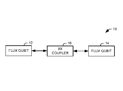
[0016] FIG. 1 illustrates one example of system 10 comprising two coupled
flux
qubits. The system includes a first flux qubit 12 and a second flux qubit 14
operatively
coupled to the first flux qubit via an XX coupler 16. A flux qubit, in general
terms, is a
superconducting loop interrupted by some number of Josephson junctions. While
a
biasing element is not illustrated in the simplified example of FIG. 1, in
general
operation, a flux qubit is biased by a flux in units of the superconducting
flux
quantum T. When the applied bias flux is near one-half of a flux quantum and
for
suitable device parameters, the potential energy of the system exhibits two
minima, one
corresponding to clockwise and the other to counterclockwise current flow in
the
superconducting loop. The two possible directions of current flow represent
the lowest
energy quantum states of the system. While it is also possible to have a
single potential
well even at half a flux quantum of bias flux, the double-well regime
described here
highlights the unique capability of the inventive coupler to function even
with
energetically degenerate states.
4
Date Recue/Date Received 2020-10-30
CA 03050915 2019-07-18
WO 2018/151929 PCT/US2018/015729
[0017] A quantum system comprising the two flux qubits 12 and 14 has four
energy minima, assuming both qubits are biased appropriately. Using 10) to
refer to a
first direction (e.g., clockwise) of current flow and 1) to apply to a second
direction (e.g.,
counter-clockwise) in the standard basis, the four states representing the
energy
minima are 100), 101), 110), and 111). The energy minima are separated by
potential
barriers, such that a transition from one minima to another generally
requires, in the
absence of quantum tunneling, application of energy to the system to bring one
or both
qubits into an excited state and then allow the excited qubit or qubits to
fall back into
one of the energy minima.
[0018] A quantum circuit can be designed such that there is a non-zero
probability that the state of a given qubit can change without the application
of energy.
In general, the Josephson junctions in a flux qubit loop create a potential
with two or
more minima and a barrier through which the multi-dimensional phase wave-
function
can tunnel. In accordance with an aspect of the present invention, the XX
coupler 16
creates a plurality of tunneling paths between the potential minima associated
with the
multiple states of the first and second flux qubits 12 and 14, such that a
tunneling path
between pairs of ground states having equal bit parity are created. In other
words, the
XX coupler 16 allows the system formed by the two qubits to tunnel between the
states
100) and 111) as well as between the states 01) and 10) . Effectively, a first
tunneling
path creates a first interaction g101)(10+10)(01), where gi is the strength,
or tunneling
energy of the first interaction, and a second tunneling path creates a second
interaction
g 2(100)011+10(000 , where g2 is the strength of the second interaction. The
interaction
strength, gi, for a given tunneling path depends on the height of the
tunneling barrier
between the two states is and is equal to half the energy splitting between
the ground
states and excited states of the coupling term. The sum of the two
interactions is the
XX interaction as written in the standard, or Z, basis.
CA 03050915 2019-07-18
WO 2018/151929 PCT/US2018/015729
[0019] An advantage of the proposed XX coupler 16 is that it can provide an
XX
interaction without coupling the qubits along other axes of the Bloch sphere
or
introducing single qubit effects, such as single qubit tunneling. When the
coupler
Josephson junctions have slightly different critical currents due to
fabrication variation,
the coupler can produce an interaction gxxXX + gyyYY gzzZZ, where the signs of
gyy
and gzz can be positive or negative depending on the relative values of the
coupler
junctions' critical currents. The magnitudes of gyy and gzz can be tuned to
zero by
replacing one or more junctions with tunable junctions, such as compound
junctions .
For example, where compound junctions are used, and the coupling strengths can
be
tuned by adjusting the flux in the compound junction loops. If the junction
variation is
small, only a single tunable junction may be needed to tune gyy and gzz to
zero. For
large junction variations, multiple junctions may be replaced with tunable
junctions to
tune gyy and gzz to zero. This also allows the XX coupling strength to be
adjusted and
even set to zero if desired. Where a pure ZZ coupling is desired, the
tunneling barriers
can be raised using a first set of control fluxes, thereby shutting off all
tunneling
between potential minima, and both 00 and 11 minima can be raised or lowered
in
energy relative to the 01 and 10 minima using a second set of control fluxes.
Further,
the proposed coupler can be used for qubits having degenerate energy states,
that is,
energy states having the same energy. Flux qubits are a common example of a
qubit
that can be operated with degenerate ground states. The inventors have found
that,
given current fabrication techniques, coupling strengths as high as two
gigahertz
between two flux qubits can be achieved via the proposed coupler.
[0020] FIG. 2 illustrates a high level schematic of a quantum circuit 30
for
generating an XX interaction. It will be appreciated that, in contrast to the
more specific
examples of FIGS. 3, 5, and 6, the illustrated circuit is provided at a
conceptual level to
better explain the concepts involved. The circuit 30 includes a first flux
qubit 32 and a
second flux qubit 34 joined by an XX coupler 40. The coupler 40 is configured
to create
a first tunneling path 42 and a second tunneling path 44 between potential
energy
6
CA 03050915 2019-07-18
WO 2018/151929 PCT/US2018/015729
minima, representing quantum states of the system including by the two flux
qubits 32
and 34. A first control mechanism 52 creates one or more control fluxes that
change
the tunneling strength along the first tunneling path 42 and the absolute
energies of
states coupled via the first tunneling path. A second control mechanism 54
creates one
or more control fluxes that change the tunneling strength along the second
tunneling
path 44 and the absolute energies of states coupled via the second tunneling
path. A
third control mechanism 56 provides voltages signals that set offset charge
values on
specific nodes of the quantum circuit, comprising both flux qubits and
coupler. The
control of offset charge enables the sign of the XX coupling to be adjusted to
either
positive or negative.
[0021] FIG. 3 is one example of a quantum circuit 70 for generating an XX
interaction between two flux qubits. In the illustrated implementation, the
two flux qubits
are not tunable, and are integrated at least partially into the coupler
assembly itself, and
the circuit 70 can be conceptualized as a single assembly with, for suitable
circuit
100)+111) 101)+110)
parameters, doubly degenerate ground states and .
Here, the state
(0 or 1) of a first flux qubit represents the direction of the current passing
through first
and second Josephson junctions 72 and 73, and a state (0 or 1) of a second
flux qubit
represents the direction of the current passing through third and fourth
Josephson
junctions 74 and 75. While, as described above, the flux qubits are integral
with the
coupler, the coupler can be considered to include fifth, sixth, seventh, and
eighth
Josephson junctions 76-79 as well as a capacitor 80. It should be noted that
any
number of junctions could be replaced with a tunable junction, such as a flux-
tunable
compound junction. Incorporating two tunable junctions is sufficient for a
high purity XX
interaction in the presence of moderate junction asymmetry. The circuit of
Fig. 3 can
also be viewed as instance of the circuit in Fig. 6 where the two junctions,
214 and 224,
have been replaced by compound junctions and tuned to nearly zero Josephson
7
CA 03050915 2019-07-18
WO 2018/151929 PCT/US2018/015729
energy. In this case the two junctions, 214 and 224, can be omitted from the
circuit,
producing the simplified circuit if Fig. 3.
[0022] Each Josephson junction 72-79 as well as the capacitor 80 has a
superconducting phase, 8, across the component. For the purpose of example,
each
of the first and second Josephson junctions 72 and 73 will be assumed to have
a same
superconducting phase of Si, each of the third and fourth Josephson junctions
74
and 75 will be assumed to have a same superconducting phase of 82. Given this
assumption, a potential, 1Jc, due to the coupler can be written as:
U c = ¨E5cos(8; +5, - 63) - E6cos(81+ 82+ 63 ¨27ifi)
Eq. 1
[0023] where E6 is a Josephson energy of the fifth Josephson junction 76,
E6 is a
Josephson energy of the sixth Josephson junction 77, E7 is a Josephson energy
of the
seventh Josephson junction 78, E8 is a Josephson energy of the eighth
Josephson
junction 79, 63 is a superconductive phase across the capacitor 80, fi is the
flux, in flux
quanta, through the loop of the assembly containing junctions 72 through 77,
f2 is the
flux, in flux quanta, through the loop of the assembly containing the
junctions 72, 73, 77,
and 78, and f3 is the flux, in flux quanta, through the loop of the assembly
containing
junctions 74, 75, 77 and 79.
[0024] For Es = E6 = E7 = E8 = E, f1 = 0, and f2 = 3= 0.5, the potential
can be
rewritten as:
Uc = 4E sin(80sin(82)cos(83) Eq. 2
[0025] This potential has the desirable property that for 63 = 0, energy
is positive
along the line Si = 82 and negative along the line 61 = ¨62. At 83 = II, the
opposite is
true ¨ energy is negative along the line 61 = 62 and positive along the line
61 = ¨62.
Now, two uncoupled flux qubits, having Josephson junctions with phase
variables 61
and 62, respectively, will have a potential with four minima at [ 6, 6], where
1601 is
the magnitude of the phase at the minima of the double well potential for each
flux qubit.
8
CA 03050915 2019-07-18
WO 2018/151929 PCT/US2018/015729
Introducing the coupler raises the energy of the two states +[60,60] relative
to the two
states [-Fe50,-T,50] at (53 = 0 and vice versa at 63 = it. Accordingly, pairs
of minima are
located in separate planes of constant 63.
[0026] FIG. 4 is an energy diagram representing the circuit of FIG. 3 in
terms of
the superconducting phases 8õ (52, and 53. In the energy diagram, the grey
shapes
represent surfaces having a same energy, and the smaller solid black shapes
represent
the four minima of the potential. The four minima are labeled based on the
sign of the
phases of Si and 62 at the minima, which determine the direction of current
flow in the
qubits. A first view 110 of the energy diagram depicts a projection of the
energy
diagram into the 52-83 plane. A horizontal axis 112 represents a value for the
superconducting phase, (52, of the Josephson junctions 74 and 75 associated
with the
second qubit, in radians divided by 2;r and a vertical axis 114 represents a
value for the
superconducting phase, 83, of the capacitor 80 associated, in radians divided
by 2.'r. It
will be appreciated that two of the minima, 101) and 110), are located on the
plane 63 =
0, and the other two minima, 100) and 111), are located on the plane
corresponding
to 63/27 = 0.5, or more simply, 63 = it.
[0027] A second view 120 of the energy diagram depicts a projection of the
energy diagram into the gi 82 plane. A horizontal axis 122 represents a value
for the
superconducting phase, 8, of the Josephson junctions 72 and 73 associated with
the
first qubit, in radians divided by 22t and a vertical axis 124 represents a
value for the
superconducting phase, 82, of the Josephson junctions 74 and 75 associated
with the
second qubit, in radians divided by 221-. It will be appreciated that two of
the minima,
101) and 110), are located on the plane 61 = ¨62, and the other two minima,
00) and 111)
are located on the plane, S = 62. A third view 130 of the energy diagram
depicts a
perspective view. As with the other views 110 and 120, a first axis 132
represents a
value for the superconducting phase, 8,, of the Josephson junctions 72 and 73
9
CA 03050915 2019-07-18
WO 2018/151929 PCT/US2018/015729
associated with the first qubit, in radians divided by 2r, a second axis 134
represents a
value for the superconducting phase, 82, of the Josephson junctions 74 and 75
associated with the second qubit, in radians divided by 2.7r, and a third axis
136
represents a value for the superconducting phase, 83, of the capacitor 80
associated, in
radians divided by 2.71.
[0028] As can be seen from the diagram, if the wave function spread is
large in
the 8 ¨ .52 plane, to enable tunnel-coupling, but small in the iS3 direction,
the desired
ground states, (100) +111))/V2 and (101) +110))/V2, will form. The strength of
the ¨XX
interaction is given by the strength of the tunnel coupling between potential
minima.
When there are multiple tunneling paths from one minima to another, it is
possible for
offset charges to affect the tunneling energy due to interference from the
Aharonov-
Casher effect. Further, it will be appreciated that a capacitance of the
capacitor 80 can
be selected to decrease the wave-function spread in one direction. This
decrease in the
spread of the wave function can decouple the two sets of minima, allowing for
the
coupler to achieve the two aforementioned ground states. It will be
appreciated that
functional coupler can also be constructed where one or more of junctions 72-
75 in
FIG. 3 are replaced with inductors of suitable value. It will also be
appreciated that, by
adding suitable inductors, this circuit can couple two flux qubits via mutual
inductance
such that the qubits and couplers are electrically isolated from each other.
[0029] FIG. 5 is another example of a quantum circuit 150, comprising a
plurality
of Joesphson junctions 151-156, for generating an XX interaction between two
flux
qubits. As in FIG. 3, the two flux qubits are not tunable, and are integrated
into the
coupler assembly itself. In general terms, however, a state of a first flux
qubit is
represented by the direction of the current passing through junction 153, and
a state of
a second flux qubit is represented by the direction of the current passing
through
junction 155. While the flux qubits are integral with the coupler, the coupler
can be
considered to include first and second Josephson junctions 151 and 152. It
will be
appreciated, however, that any number of junctions could be replaced with a
compound
CA 03050915 2019-07-18
WO 2018/151929 PCT/US2018/015729
Josephson junction or other element having a tunable Josephson energy.
Incorporating
tunable junctions is sufficient for a high purity XX interaction in the
presence of junction
asymmetry, for example, due to minor variances in the fabrication process.
[0030] FIG. 6 is yet another example of a quantum circuit 200 for
generating an
XX interaction between two flux qubits 210 and 220. In the illustrated
implementation,
each flux qubit 210 and 220 is tunable via an applied flux, such that either
or both of a
relative energy of the energy levels of the qubit and a barrier height between
the energy
states can be tuned. A first flux qubit 210 comprises three Josephson
junctions 212-214 arranged in a loop enclosing nominally one half of a flux
quantum. A
second flux qubit 220 comprises three Josephson junctions 222-224 arranged in
a loop
enclosing nominally one half of a flux quantum.
[0031] A coupler 230 comprises a first Josephson junction 232 connected to
each
of the first reference node 216 and the fourth reference node 226, and a
second
Josephson junction 233 connected to each of the second reference node 217 and
the
fifth reference node 227. A third Josephson junction 234 is connected to each
of the
first reference node 216 and the fifth reference node 227, and a fourth
Josephson
junction 235 is connected to each of the second reference node 217 and the
fourth
reference node 226, such that the coupler forms a "twisted loop" comprising
the four
Josephson junctions. A capacitor 238 is connected to each of the third
reference
node 218 and the sixth reference node 228.
[0032] It will be appreciated that the Josephson energy of a Josephson
junction is
generally static. In one implementation, one or more of the Josephson
junctions 232-235 comprising the coupler 230 can be replaced with a tunable
element
having a Josephson energy that is tunable via an applied flux or other control
signal.
One example of such an element is a compound Josephson junction. In practice,
at
least one tunable junction is advisable to correct for variance in the
fabrication process
even under the best of circumstance, and in practice, two tunable junctions
can be used
for this purpose. In one implementation, all of the Josephson junction 232-235
can be
11
CA 03050915 2019-07-18
WO 2018/151929 PCT/US2018/015729
made tunable such that the tunneling energies of the tunneling paths created
by the
coupler can be tuned to alter or eliminate the coupling provided by the
device. For
example, the tunneling energies can be reduced to near zero to eliminate the
XX
coupling or made unequal to add an element of ZZ coupling. In another
implementation,
the capacitor 238 can be omitted and offset charges, controlled by gate
voltages, can
be used to suppress undesired tunneling and control the sign of the coupling.
This is
possible via Aharonov-Casher interference, whereby offset charge on a
superconducting island in the circuit induces a phase difference between two
tunneling
paths from on minimum to another. When the offset charge is 0.5 Cooper pairs,
the
interference is destructive and tunneling does not occur. When the offset
charge is
between 0.5 and 1 Cooper pair, the tunneling energy can be negative leading to
an anti-
symmetric ground state as is the case for a positive XX coupling.
[0033] In view of the foregoing structural and functional features
described above
in FIGS. 1-6, example methods will be better appreciated with reference to
FIG. 7.
While, for purposes of simplicity of explanation, the method of FIG. 7 is
shown and
described as executing serially, it is to be understood and appreciated that
the present
invention is not limited by the illustrated order, as some actions could in
other examples
occur in different orders and/or concurrently from that shown and described
herein.
[0034] FIG. 7 illustrates one example of a method 300 for coupling quantum
states of two flux qubits. At 302, a first flux qubit is electrically coupled
to a second flux
qubit via a coupler comprising a plurality of Josephson junctions, with at
least one being
tunable, in addition to capacitive and/or mutual inductive and/or galvanic
interactions.
The coupler creates a first tunneling path, between a first pair of energy
minima
associated with a system formed by the first and second qubit, and a second
tunneling
path, between a second pair of energy minima associated with the system. In
one
implementation, tunneling paths are formed between minima representing states
of the
system having equal bit parity, that is, between the states 100) and 11) and
between
the states 101) and 110).
12
CA 03050915 2019-07-18
WO 2018/151929 PCT/US2018/015729
[0035] At 304, a control signal, such as current, producing flux or
voltage, is
applied to at least one of the one or more tunable junctions to select a first
tunneling
energy associated with the first tunneling path and a second tunneling energy
associated with the second tunneling path. In accordance with an aspect of the
present
invention, the selection of the tunneling energies via the applied signal can
control the
coupling behavior of the coupler. For example, if the control signal is
applied such that
the first and second coupling energies are substantially equal, an XX coupling
between
the first flux qubit and the second flux qubit is produced. To maintain a pure
XX
coupling, one or more other tunable Josephson junctions may be adjusted with a
control
signal to ensure that single qubit tunneling effects and YY and ZZ couplings
are
avoided. In another example, the control signal can be applied such that the
first and
second coupling energies are not equal to provide an XX coupling, a YY
coupling and/or
a ZZ coupling between the first flux qubit and the second flux qubit. Finally,
the control
signal can be applied such that the first and second coupling energies are
substantially
equal to zero as to selectively decouple the first flux qubit and the second
flux qubit.
Accordingly, the coupling provided by the coupler can be controlled for
quantum logic
gate operations and other applications.
[0036] What have been described above are examples of the present
invention.
It is, of course, not possible to describe every conceivable combination of
components
or methodologies for purposes of describing the present invention, but one of
ordinary
skill in the art will recognize that many further combinations and
permutations of the
present invention are possible. Accordingly, the present invention is intended
to
embrace all such alterations, modifications, and variations that fall within
the scope of
the appended claims.
13