Note: Descriptions are shown in the official language in which they were submitted.
85444147
PROVIDING SINGLE DATA RATE (SDR) MODE OR DOUBLE DATA RATE (DDR)
MODE FOR THE COMMAND AND ADDRESS (CA) BUS OF REGISTERING CLOCK
DRIVE (RCD) FOR DYNAMIC RANDOM ACCESS MEMORY (DRAM)
[0001]
TECHNICAL FIELD
[0002] This disclosure relates generally to the field of command and
address (CA) bus
of memory devices, and, in particular, to providing single data rate (SDR)
mode or double data
rate (DDR) mode for the command and address (CA) bus of a registering clock
drive (RCD) for
a dynamic random access memory (DRAM).
BACKGROUND
[0003] Dynamic Random Access Memory (DRAM) technology may utilize Dual Data
Rate (DDR) mode on the addressing mechanism, e.g., command/address (CA) input
bus of the
Registering Clock Drive (RCD) from a host and Single Data Rate (SDR) mode on
the CA
output bus of the RCD to the DRAM device. In one example, the CA input bus may
be routed
on a lengthy signal path from the host to the RCD input. However, due to the
path length, path
noise, path attenuation, and path reflection (e.g., impedance mismatch), the
signal integrity of
the CA input bus may be severely compromised, especially as the clock rate
increases.
[0004] For example, signal integrity degradations may limit clock frequency
scaling
(i.e., running the clock frequency at a higher rate) to improve overall
processing system
performance. In addition, signal integrity degradations may result in sub-
optimal signal
calibration during DRAM initialization. Also, signal integrity degradation may
worsen as
multiple memory devices (e.g., DRAMs) are installed with a common CA bus,
which may
increase bus loading and lead to further signal integrity degradation. Thus,
there is a need for
improved storage element architectures which preserve signal integrity
requirements for a
memory control path (e.g., CA bus) as the clock frequency increases.
1
Date Recue/Date Received 2021-03-18
CA 03051008 2019-07-19
WO 2018/156780
PCMJS2018/019251
SUMMARY
[0005] The
following presents a simplified summary of one or more aspects of the
present disclosure, in order to provide a basic understanding of such aspects.
This summary is
not an extensive overview of all contemplated features of the disclosure, and
is intended neither
to identify key or critical elements of all aspects of the disclosure nor to
delineate the scope of
any or all aspects of the disclosure. Its sole purpose is to present some
concepts of one or more
aspects of the disclosure in a simplified form as a prelude to the more
detailed description that
is presented later.
[0006] In one
aspect, the disclosure provides mode selection. Accordingly, a method for
providing a single data rate (SDR) mode or a double data rate (DDR) mode to a
Registering
Clock Drive (RCD) for a memory, including determining one or more data rate
mode selection
criteria; selecting a data rate mode based on the one or more data rate mode
selection criteria;
configuring a host interface for the data rate mode; and configuring an RCD
input interface of
the Registering Clock Drive (RCD) for the data rate mode.
[0007] In one
example, the data rate mode is one of the SDR mode or the DDR mode.
In one example, the host interface is an output of a host for connection to
the Registering Clock
Drive (RCD) via an input bus. In one example, the RCD input interface is an
input of the
Registering Clock Drive (RCD) for connection to the host via the input bus. In
one example,
the data rate mode is set at initialization and remains static throughout a
session. In one
example, the data rate mode is variable between the SDR mode and the DDR mode
throughout
a session.
[0008] In one
example, the method further includes transferring data between the host
interface and the RCD input interface using a clock signal. In one example,
the transferring data
includes a WRITE operation. In one example, the transferring data includes a
READ operation.
In one example, the data includes a command or an address.
[0009] In one
example, the method further includes transferring the data from an RCD
output interface using the clock signal in either 1N mode or 2N mode. In one
example, the RCD
output interface is an output of the RCD to the memory via an output bus. In
one example, the
memory is a dynamic random access memory (DRAM).
[0010] In one
example, the method further includes activating the clock signal on the
host interface and on the RCD input interface. In one example, the method
further includes
configuring the host interface to initiate a data transfer on the host
interface using a clock
2
CA 03051008 2019-07-19
WO 2018/156780
PCT/US2018/019251
signal. In one example, the method further includes configuring the RCD input
interface to
initiate a data reception on the RCD input interface using the clock signal.
In one example, the
one or more data rate mode selection criteria include at least one of a clock
speed, a burst
length, an access statistic, a read/write ratio, a latency, a duty factor, a
page clustering, a
streaming characteristic, a dc power constraint, or a data traffic
characteristic quantified using
an address correlation metric.
[0011] Another
aspect of the disclosure provides an apparatus for providing a single
data rate (SDR) mode or a double data rate (DDR) mode to a Registering Clock
Drive (RCD)
for a memory, the apparatus including a memory controller, wherein the memory
controller
determines one or more data rate mode selection criteria, selects a data rate
mode based on the
one or more data rate mode selection criteria, configures a host interface for
the data rate mode
and configures an RCD input interface for the data rate mode; a clock
generator coupled to the
memory controller, wherein the clock generator activates a clock signal on the
host interface
and on the RCD input interface; and a host coupled to the memory controller,
wherein the host
transfers data between the host interface and the RCD input interface using
the clock signal.
[0012] In one
example, the apparatus further includes a Registering Clock Drive (RCD)
coupled to the memory controller, wherein the RCD transfers the data from an
RCD output
interface using the clock signal in either IN mode or 2N mode. In one example,
the host
includes the host interface and the Registering Clock Drive (RCD) includes the
RCD input
interface and the RCD output interface. In one example, the data rate mode is
one of the SDR
mode or the DDR mode. In one example, the data rate mode is set at
initialization and remains
static throughout a session. In one example, the data rate mode is variable
between the SDR
mode and the DDR mode throughout a session.
[0013] Another
aspect of the disclosure provides an apparatus for providing a single
data rate (SDR) mode or a double data rate (DDR) mode to a Registering Clock
Drive (RCD)
for a memory, including means for determining one or more data rate mode
selection criteria;
means for selecting a data rate mode based on the one or more data rate mode
selection criteria;
means for configuring a host interface for the data rate mode; and means for
configuring an
RCD input interface of the Registering Clock Drive (RCD) for the data rate
mode.
[0014] In one
example, the apparatus further includes means for activating a clock
signal on the host interface and on the RCD input interface; and means for
transferring data
from the host interface to the RCD input interface using the clock signal. In
one example, the
apparatus further includes means for transferring the data from an RCD output
interface using
3
85444147
the clock signal in either 1N mode or 2N mode. In one example, the data rate
mode is one of
the SDR mode or the DDR mode.
[0015] Another aspect of the disclosure provides a computer-readable
medium
storing computer executable code, operable on a device including at least one
processor and at
least one memory coupled to the at least one processor, wherein the at least
one processor is
configured to provide a single data rate (SDR) mode or a double data rate
(DDR) mode to a
Registering Clock Drive (RCD) for a memory, the computer executable code
including:
instructions for causing a computer to determine one or more data rate mode
selection criteria;
instructions for causing the computer to select a data rate mode based on the
one or more data
rate mode selection criteria; instructions for causing the computer to
configure a host interface
for the data rate mode; and instructions for causing the computer to configure
an RCD input
interface of the Registering Clock Drive (RCD) for the data rate mode.
[0016] In one example, the computer-readable medium further includes
instructions
for causing the computer to activate a clock signal on the host interface and
on the RCD input
interface; instructions for causing the computer to transfer data from the
host interface to the
RCD input interface using the clock signal, and wherein the data rate mode is
one of the SDR
mode or the DDR mode; and instructions for causing the computer to transfer
the data from an
RCD output interface using the clock signal in either 1N mode or 2N mode.
[0016a] According to one aspect of the present invention, there is
provided a method
for providing a single data rate (SDR) mode or a double data rate (DDR) mode
to a
Registering Clock Drive (RCD) for a memory, comprising: determining one or
more data rate
mode selection criteria; selecting a data rate mode for a command/address (CA)
bus based on
the one or more data rate mode selection criteria, wherein the one or more
data rate mode
selection criteria include one of an access statistic or a data traffic
characteristic quantified
using an address correlation metric; configuring a host interface for the data
rate mode; and
configuring an RCD input interface of the Registering Clock Drive (RCD) for
the data rate
mode.
[0016b] According to another aspect of the present invention, there is
provided an
apparatus for providing a single data rate (SDR) mode or a double data rate
(DDR) mode to a
Registering Clock Drive (RCD) for a memory, the apparatus comprising: a memory
controller, wherein the memory controller determines one or more data rate
mode selection
4
Date Recue/Date Received 2021-03-18
85444147
criteria, selects a data rate mode for a command/address (CA) bus based on the
one or more
data rate mode selection criteria, configures a host interface for the data
rate mode and
configures an RCD input interface for the data rate mode, wherein the one or
more data rate
mode selection criteria include one of an access statistic or a data traffic
characteristic
quantified using an address correlation metric; a clock generator coupled to
the memory
controller, wherein the clock generator activates a clock signal on the host
interface and on the
RCD input interface; and a host coupled to the memory controller, wherein the
host transfers
data between the host interface and the RCD input interface using the clock
signal.
[0016c] According to still another aspect of the present invention, there
is provided an
apparatus for providing a single data rate (SDR) mode or a double data rate
(DDR) mode to a
Registering Clock Drive (RCD) for a memory, comprising: means for determining
one or
more data rate mode selection criteria; means for selecting a data rate mode
for a
command/address (CA) bus based on the one or more data rate mode selection
criteria,
wherein the one or more data rate mode selection criteria include one of an
access statistic or a
data traffic characteristic quantified using an address correlation metric;
means for
configuring a host interface for the data rate mode; and means for configuring
an RCD input
interface of the Registering Clock Drive (RCD) for the data rate mode.
[0016d] According to yet another aspect of the present invention, there
is provided a
computer-readable medium storing computer executable code, operable on a
device
comprising at least one processor and at least one memory coupled to the at
least one
processor, wherein the at least one processor is configured to provide a
single data rate (SDR)
mode or a double data rate (DDR) mode to a Registering Clock Drive (RCD) for a
memory,
the computer executable code comprising: instructions for causing a computer
to determine
one or more data rate mode selection criteria; instructions for causing the
computer to select a
data rate mode for a command/address (CA) bus based on the one or more data
rate mode
selection criteria wherein the one or more data rate mode selection criteria
include one of an
access statistic or a data traffic characteristic quantified using an address
correlation metric;
instructions for causing the computer to configure a host interface for the
data rate mode; and
instructions for causing the computer to configure an RCD input interface of
the Registering
Clock Drive (RCD) for the data rate mode.
4a
Date Recue/Date Received 2021-03-18
85444147
[0017]
These and other aspects of the invention will become more fully understood
upon a review of the detailed description, which follows. Other aspects,
features, and
embodiments of the present invention will become apparent to those of ordinary
skill in the
art, upon reviewing the following description of specific, exemplary
embodiments of the
present invention in conjunction with the accompanying figures. While features
of the present
invention may be discussed relative to certain embodiments and figures below,
all
embodiments of the present invention can include one or more of the
advantageous features
discussed herein. In other words, while one or more embodiments may be
discussed as having
certain advantageous features, one or more of such features may also be used
in accordance
with the various embodiments of the invention discussed herein. In similar
fashion, while
exemplary embodiments may be discussed below as device, system, or method
embodiments
it should be understood that such exemplary embodiments can be implemented in
various
devices, systems, and methods.
BRIEF DESCRIPTION OF THE DRAWINGS
4b
Date Recue/Date Received 2021-03-18
CA 03051008 2019-07-19
WO 2018/156780
PCT/US2018/019251
[0018] FIG. 1
illustrates an example memory system showing signaling between a
memory controller and memory.
[0019] FIG. 2
illustrates an example memory system with a Registering Clock Device
(RCD) between a host and a memory.
[0020] FIG. 3
illustrates an example of a two channel RCD with two input buses and
four output buses.
[0021] FIG. 4
illustrates an example of a one unit interval (UI) timing diagram in Single
Data Rate (SDR) mode.
[0022] FIG. 5
illustrates an example of a two unit interval (U1) timing diagram in Single
Data Rate (SDR) mode.
[0023] FIG. 6
illustrates an example flow diagram for selecting and executing a data
rate mode for a command/address (CA) bus for a Registering Clock Drive (RCD)
for a
Dynamic Random Access Memory (DRAM).
DETAILED DESCRIPTION
[0024] The
detailed description set forth below in connection with the appended
drawings is intended as a description of various aspects of the present
disclosure and is not
intended to represent the only aspects in which the present disclosure may be
practiced. Each
aspect described in this disclosure is provided merely as an example or
illustration of the
present disclosure, and should not necessarily be construed as preferred or
advantageous over
other aspects. The detailed description includes specific details for the
purpose of providing a
thorough understanding of the present disclosure. However, it will be apparent
to those skilled
in the art that the present disclosure may be practiced without these specific
details. In some
instances, well-known structures and devices are shown in block diagram form
in order to avoid
obscuring the concepts of the present disclosure. Acronyms and other
descriptive terminology
may be used merely for convenience and clarity and are not intended to limit
the scope of the
present disclosure.
[0025] While for
purposes of simplicity of explanation, the methodologies are shown
and described as a series of acts, it is to be understood and appreciated that
the methodologies
are not limited by the order of acts, as some acts may, in accordance with one
or more aspects,
occur in different orders and/or concurrently with other acts from that shown
and described
herein. For example, those skilled in the art will understand and appreciate
that a methodology
could alternatively be represented as a series of interrelated states or
events, such as in a state
CA 03051008 2019-07-19
WO 2018/156780
PCT/US2018/019251
diagram. Moreover, not all illustrated acts may be required to implement a
methodology in
accordance with one or more aspects.
[0026] A dynamic
random access memory (DRAM) device is commonly used as a
storage element in processing systems, such as personal computers (PCs),
laptop computers,
mobile devices, personal digital assistants (PDAs), etc. A DRAM may include a
plurality of
memory cells, where each memory cell may include a transistor and a capacitor
to store a single
bit of information. A DRAM may be used for at least two types of data transfer
operations, a
WRITE operation and a READ operation. A DRAM may store a plurality of bits
into memory,
a WRITE operation, using WRITE data lines to transfer bits from a data source
to the DRAM
data input ports for data storage into memory. Also, a DRAM may retrieve a
plurality of bits
from memory, a READ operation, using READ data lines to transfer bits from the
DRAM data
output ports to a data destination for data retrieval from memory. The WRITE
and READ
operations may be controlled via a separate control path, for example, a
command/address (CA)
bus. Commands are a set of bit patterns which designate a desired operation or
state, for
example, WRITE, READ, CLEAR, RESET, etc. An address is a specific group of bit
patterns
which designates a desired memory location for either a WRITE operation or a
READ
operation. Note that the quantity of bits in an address bit pattern does not
necessarily equal the
quantity of bits transferred in either a WRITE or READ operation.
[0027] Generally,
a data transfer operation in a processing system occurs between a host
and a storage element. A host may include a processor (e.g., central processor
unit (CPU),
microprocessor, microcontroller, multiprocessor, etc.). In one example, the
control path (e.g.,
CA bus) from a host to a storage element (e.g., DRAM) may require an
intermediary device
(e.g., a Registering Clock Drive (RCD)) for signal conditioning. Signal
conditioning may
include, for example, buffering, signal registration, re-clocking, re-driving,
etc. The RCD may
be part of the storage element, for example, a DRAM, or may be one component
in a memory
module, for example, a dual inline memory module (DIMM).
[0028] A memory
device (e.g., DRAM) may use a clock signal, for example, a periodic
square wave reference signal (e.g., with alternating low and high levels), to
regulate
synchronous operation of the DRAM. A clock signal may include a plurality of
repeating clock
cycles. In general, a DRAM may function in a variety of modes, for example,
data rate modes.
Two used data rate modes are single data rate (SDR) mode and dual data rate
(DDR) mode.
Data rate modes may be used for the control path (e.g., CA bus). For example,
in SDR mode,
data are transferred only on either a rising edge (i.e., low/high transition)
or a falling edge (i.e.,
6
CA 03051008 2019-07-19
WO 2018/156780
PCT/1JS2018/019251
high/low transition) of a clock cycle. That is, a data transfer operation
occurs only once per
clock cycle. In DDR mode, data are transferred on both the rising edge and
falling edge of the
clock cycle. That is, data transfer operations occur twice per clock cycle.
[0029] DRAM
technology has evolved over time to achieve progressively more capable
memory devices. For example, DRAM technology has progressed from DDR1 through
DDR2,
DDR3, DDR4, DDR5, etc. DRAM interface requirements are specified by industry
standards
bodies, for example, Joint Electron Device Engineering Council (JEDEC), to
ensure device
compatibility among different vendors.
[0030] A form of
volatile memory (i.e., storage element) is a Dynamic Random Access
Memory (DRAM). A host (e.g., computer, processor, controller, etc.) may employ
the DRAM
for rapid storage and retrieval of data and instructions. Data may be stored
and/or retrieved in
the DRAM using an addressing mechanism (e.g., memory control path) to specify
a DRAM
location for data storage or data retrieval. One type of memory control path
is a
command/address (CA) bus. In some cases, an intermediary device, known as a
Registering
Clock Drive (RCD), mediates between the host and DRAM by providing signal
conditioning.
The RCD has an input CA bus and an output CA bus. One form of mediation is
data rate mode
mediation. Two used DRAM data rate modes are single data rate (SDR) mode and
dual data
rate (DDR) mode.
[0031] FIG. 1
illustrates an example memory system 100 showing signaling between a
memory controller and memory. Shown in FIG. 1 are two elements, a memory
controller 110
and a memory 120. Also shown in FIG. 1 are three signal paths between the
memory controller
110 and the memory 120: a) a command/address (CA) bus 130; b) a data bus 140;
and c) a
clock signal 150. In one example, the memory controller 110 is part of a host
which either
sends data on data bus 140 to the memory 120 as part of a WRITE operation or
receives data on
data bus 140 from the memory 120 as part of READ operation. The
command/address (CA) bus
130 may be used to execute the 'WRITE or READ operations and to specify the
desired memory
address for either operation. In addition, the clock signal 150 may be used to
pace the WRITE
and READ operations synchronously. In one example, the clock signal 150 is
generated by a
clock generator 160 which is coupled to the memory controller 110. In another
example,
although not shown, the clock generator 160 may be coupled directly to the
memory 120. In
another example, the clock generator 160 may be couple to either or both of
the memory
controller 110 and memory 120 through a clock distribution circuit (not
shown).
7
CA 03051008 2019-07-19
WO 2018/156780
PCT/US2018/019251
[0032] FIG. 2
illustrates an example memory system 200 with a Registering Clock
Device (RCD) 220 between a host 210 and a memory 230. In one example, the
memory 230 is
Dynamic Random Access Memory (DRAM). Shown in FIG. 2 are a control/address
(CA) input
bus 240 and a control/address (CA) output bus 250. The host 210 may include a
host interface
which is an output of the host 210 connected to the CA input bus 240 which is
inputted to the
RCD 220. The RCD 220 may include an RCD input interface which is an input to
the RCD
connected to the CA input bus 240 from the host 210. The host interface and
the RCD input
interface allow interconnection between the host 210 and the RCD 220 using the
CA input bus
240. The RCD 220 may include an RCD output interface which is an output to the
memory 230
via the CA output bus 250 to the memory 230.
[0033] The CA
input bus 240 with (N+p) bits delivers command data and address input
data from the host 210 to the RCD 220. N denotes the quantity of bits being
transferred over the
CA input bus and p denotes the quantity of parity bits over the CA input bus.
For example, p=0
denotes a no parity case, p = 1 denotes a single parity case, p = 2 denotes a
double parity case,
etc. The CA output bus 250 with (2N+q) bits delivers command output data and
address output
data from the RCD 220 to the memory 230. 2N denotes the quantity of bits being
transferred
over the CA output bus and p denotes the quantity of parity bits over the CA
output bus. The
CA output bus may add parity bits (i.e., q # 0) or may not add parity bits
(i.e., q = 0). Also, a
mode select control line 260 is shown as a mode select input to the RCD. In
one example, the
mode select control line 260 may be used to select a data rate mode for the CA
input bus 240.
For example, the data rate modes may be Single Data Rate (SDR), Double Data
Rate (DDR),
Quadruple Data Rate (QDR), etc. In one example, the data rate mode may be set
at initialization
and may remain static for a session. In another example, the data rate mode
may be variable
over a session. That is, the data rate mode may vary between the SDR mode and
the DDR
mode. In one example, a session is a time duration for execution for a group
of operational
steps. For example, a session may be a time duration between a user login and
user logout.
[0034] In one
example, data rate mode selection may allow optimization of operational
scenarios. For example, data rate mode selection may optimize selection of
either SDR mode or
DDR mode dependent on a variety of operational scenarios. In one aspect, data
rate mode
selection may be based on clock speed, burst lengths, dc power constraints,
data traffic
characteristics, access statistics, read/write ratio, latency, duty factor,
page clustering, and/or
streaming characteristics. For example, the data rate mode may be selected
depending on clock
speed since DDR mode operation may be restricted by a maximum DDR mode clock
speed
8
CA 03051008 2019-07-19
WO 2018/156780
PCT/1JS2018/019251
(e.g.. due to limited higher speed scaling in DDR mode). For example, the data
rate mode may
be selected depending on burst length since a longer burst length provides a
higher data transfer
rate such that SDR mode may be optimal. For example, the data rate mode may be
selected
depending on dc power constraints since DDR mode operation may consume more dc
power
than SDR mode. For example, the data rate mode may be selected depending on
access
statistics or data traffic characteristics (e.g., random access or clustered
(correlated) access). In
one example, random access may be more appropriate with DDR mode and clustered
access
may be more appropriate with SDR mode. In one example, data traffic
characteristics may be
quantified using an address correlation metric. An address correlation metric
quantifies
randomness in sequential memory accesses. In one example the address
correlation metric is a
normalized value ranging from 0 to 1, where 0 denotes totally uncorrelated
sequential memory
accesses (e.g., random access) and 1 denotes totally correlated sequential
memory accesses
(e.g., clustered memory access).
[0035] In one
example, data rate mode selection may allow more relaxed timing
constraints, dc power savings, reduced channel characterization training time
(e.g., equalizer
training), etc. when SDR mode is selected. For example, more relaxed timing
constraints may
include a more relaxed interface setup and hold time, for example, relaxing
from a half clock
cycle in DDR mode to a full clock cycle in SDR mode. In one example, this
relaxed timing
constraint facilitates scaling to a higher clock speed and in achieving tight
clock skew
requirements. Moreover, in one example, board constraints may not allow usage
of DDR mode.
[0036] FIG. 3
illustrates an example of a two channel RCD 300 with two CA input
buses and four CA output buses. In the example of FIG. 3, two CA input buses
are shown
(DOCA 320 and D1CA 330), and four CA output buses are shown (QOACA 340, QOBCA
350,
QIACA 360, and Q1BCA 370). Each channel of the RCD 300 may include one CA
input bus
and two CA output buses. For example; a first channel may include DOCA 320 for
a CA input
bus and QOACA 340 and QOBCA 350 for two CA output buses. For example, a second
channel
may include DICA 330 for a CA input bus and Q1ACA 360 and QIBCA 370 for two CA
output buses. In one example, the CA input buses each include N bits and the
CA output buses
each include 2N bits. The CA input buses may also include input parity bits of
length p bits;
that is, p = 0, p = 1 or p> 1. And, the CA output buses may include output
parity bits of length
q; that is, q = 0, q = 1 or q> 1. In one example, the CA input bus may operate
in either SDR
mode or DDR mode, and the CA output bus may operate in SDR mode. For the CA
output bus,
SDR mode may also be denoted as 2N mode. In 2N mode, data is transferred only
on every
9
CA 03051008 2019-07-19
WO 2018/156780
PCT/US2018/019251
other clock edge, for example, every other rising edge. In IN mode, data is
transferred on every
clock edge; for example, every rising edge.
[0037] In one
example; the RCD 300 supports two input data rate modes, SDR (single
data rate) mode and DDR (double data rate) mode, on the CA input bus (i.e.,
facing the host) to
control the registration of bits on the CA input bus. For example, the input
data rate mode may
be selected using a mode select control line to the RCD. An example of a mode
select control
line is illustrated in FIG. 2 as the mode select control line 260. In another
example, the input
data mode may be selected by programming a mode control bit in the RCD. The
mode control
bit is programmed, for example, via a command on the CA input bus.
[0038] In one
example, a default state of the mode select control line is SDR mode. In
one example, the default state is a system state that is employed if no
explicit command is used
to set the system state. The CA input bus has a bit width of N bits. In one
example, N = 7. As an
example, a single input parity bit or multiple input parity bits may be added
to the CA input
bus, beyond N bits. That is, p = 1 or p> 1. The CA output bus has a bit width
of 2N bits. In one
example, 2N = 14. As an example, output parity bits may not be added to the CA
output bus;
that is, q = 0. Or, output parity bits may be added to the CA output bus; that
is, q = 1 or q> 1.
In an example, the RCD may expand the bit width of the CA input bus from N
bits to 2N bits
on the CA output bus.
[0039] Table 1
illustrates one possible mapping of the CA input bus bits (a.k.a., DCA)
to the CA output bus bits (a.k.a., QCA). For example, the CA input bus bits
may be individually
designated as input bit zero, input bit one, input bit two, etc., where input
bit zero may be the
least significant bit (LSB) of the CA input bus bits. For example, DCAO may
refer to input bit
zero of either DOCA or D1CA, DCA1 may refer to input bit one of either DOCA or
D1CA,
DCA2 may refer to input bit two of either DOCA or D1CA, etc. For example, the
CA output
bus bits may be individually designated as output bit zero, output bit one,
output bit two, etc.,
where output bit zero may be the least significant bit (LSB) of the CA output
bus bits. For
example, QCAO may refer to output bit zero of either QOCA or Q1CA, QCAI may
refer to
output bit one of either QOCA or Q1CA. QCA2 may refer to output bit two of
either QOCA or
Q 1CA, etc.
CA 03051008 2019-07-19
WO 2018/156780
PCT/US2018/019251
Table 1
Ul DCAO DCA1 DCA2 DCA3 DCA4 DCA5 DCA6
0 QCAO QCA1 QCA2 QCA3 QCA4 QCA5 QCA6
1 QCA7 QCA8 QCA9 QCA10 QCAll QCA12 QCA13
[0040] Also, in one example UI denotes Unit Interval, also known as a
symbol duration
time. For example, one UI is a minimum time interval between signal state
changes (e.g., pulse
time or symbol duration time) where one UI is the time taken by each
successive pulse or
symbol. In one example, Table 1 shows a mapping of input data to output data,
where there
may be 7 bits of input data (e.g., DCA) and 14 bits of output data (e.g.,
QCA). For example, the
input data (e.g., DCA) may be transferred over two UIs labeled as UI 0 and UI
1. For example,
input data from UI 0 may generate a first subset of output data (e.g., QCA 0 -
QCA 6) and input
data from UI 1 may generate a second subset of output data (e.g., QCA 7 - QCA
13).
[0041] For example, in SDR mode for the CA input bus (i.e., DCA), the mode
select
control line remains at SDR mode for the host interface and the CA output bus
(i.e., QCA)
operates in 2N mode when the SDR mode is enabled on the CA input bus (DCA). In
this case,
an advantage may be that the RCD obtains more setup and hold time on the CA
output bus in
2N mode, which improves signal integrity margin.
[0042] In one example, there may be an additional half cycle clock delay on
the CA
output bus in SDR mode since data is captured on a next rising edge of the
clock signal instead
of a next falling edge of the clock signal. In one example, the performance
impact of this delay
is minimal since read latency is typically tens of clock cycles. In addition,
CA output bus
utilization rate may be doubled in SDR mode, but the performance impact is
minimal since it
typically takes eight clock cycles to transfer data for each command to a
DRAM.
[0043] FIG. 4 illustrates an example of a one unit interval (UI) timing
diagram 400 in
Single Data Rate (SDR) mode. In the example of FIG. 4, a command or address is
transferred
over one UI, where one UI represents a symbol duration time. An input clock
DCK_t and its
complement DCK_c are shown at the top of FIG. 4 with the clock rising edge
denoted with an
uprising arrow. An input chip select signal DCS_n is used to select a chip for
a memory input
operation. A command or address is transferred using an input CA bus signal
DCA. In one
example, DCA has 7 input bits, denoted as DCA[6:0]. Parity for the input CA
bus signal may
be conveyed using a parity signal DPAR (not shown). An output clock QCK_t and
its
complement QCK_c are also illustrated. An output chip select signal QCS_n is
used to select a
11
CA 03051008 2019-07-19
WO 2018/156780
PCT/US2018/019251
chip for a memory output operation. A command or address is transferred using
an output CA
bus signal QCA. In one example, QCA has 14 output bits, denoted as DCA[13:0].
In one
example, QCA transfers data every clock cycle, i.e., once per UI.
[0044] FIG. 5
illustrates an example of a two unit interval (UI) timing diagram 500 in
Single Data Rate (SDR) mode. In the example of FIG. 5, a command or address is
transferred
over two UIs, where one UI represents a symbol duration time. An input clock
DCK t and its
complement DCK_c are shown at the top of FIG. 5 with the clock rising edge
denoted with an
uprising arrow. An input chip select signal DCS_n is used to select a chip for
a memory input
operation. A command or address is transferred using an input CA bus signal
DCA. In one
example, DCA has 7 input bits, denoted as DCA[6:0]. Parity for the input CA
bus signal may
be conveyed using a parity signal DPAR (not shown). An output clock QCK_t and
its
complement QCK_c are also illustrated. An output chip select signal QCS_n is
used to select a
chip for a memory output operation. A command or address is transferred using
an output CA
bus signal QCA. In one example, QCA has 14 output bits, denoted as DCA[13:01.
In one
example, QCA transfers data every- other clock cycle, i.e., once per 2 UI.
[0045] Table 2
illustrates the characteristics of the propagation delay tPDM through the
Registering Clock Drive (RCD).
Table 2
Symbol Parameters Conditions Min Max Unit
tPDM Propagation delay, single bit TBD V TBD TBD ns
(1,2) switching, CK_t/CK_c falling operation
edge cross point to output
I. tPDM is defined for OnCK command latency adder.
2. tPDM for SDR mode is measured from CK_UCK_c rising edge cross point to
output.
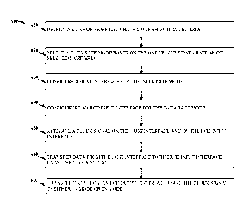
[0046] FIG. 6
illustrates an example flow diagram 600 for selecting and executing a
data rate mode for a command/address (CA) bus for a Registering Clock Drive
(RCD) for a
Dynamic Random Access Memory (DRAM). In block 610, determine one or more data
rate
mode selection criteria. In one aspect, the data rate mode selection criteria
may be based on
memory features and/or application needs. Examples of memory features may
include clock
speed and/or burst lengths. Examples of application needs may include access
statistics,
read/write ratio, latency, duty factor, page clustering, and/or streaming
characteristics. In one
12
CA 03051008 2019-07-19
WO 2018/156780
PCT/US2018/019251
example, the data rate mode selection criteria may include dc power
constraints and/or data
traffic characteristics.
[0047] For
example, for clock speeds beyond a speed threshold value, DDR mode may
not be feasible and a data rate mode selection criterion may be based on the
clock speed. In one
example, if the clock speed exceeds the speed threshold value, select SDR
mode. If the clock
speed does not exceed the speed threshold value, select DDR mode. In one
example, the speed
threshold value may be 4.8 Gigatransfers per sec (Gips).
[0048] For
example, the data rate mode selection criterion may be based on a burst
length. In one example if the burst length is greater than or equal to a burst
length threshold
value, select SDR mode. If the burst length is less than a burst length
threshold value, select
DDR mode. In one example, the burst length threshold value is 16 clock cycles.
In another
example, the burst length threshold value is 32 clock cycles. In one example,
the burst length is
a group of symbols (measured in clock cycles) transferred on the CA input bus
240 (shown in
FIG. 2).
[0049] For
example, the data rate mode selection criterion may be based on data traffic
characteristics or access statistics, such as an address correlation metric.
An address correlation
metric quantifies randomness in sequential memory accesses. In one example the
address
correlation metric is a normalized value ranging from 0 to 1, where 0 denotes
totally
uncorrelated sequential memory accesses (e.g., random access) and 1 denotes
totally correlated
sequential memory accesses (e.g., clustered memory access). In one example,
define an address
correlation metric threshold for the data rate mode selection criterion. For
example, if the
address correlation metric exceeds the address correlation metric threshold,
select SDR mode.
Otherwise, select DDR mode. In one example, the step in block 610 is performed
by a memory
controller (e.g., memory controller 110).
[0050] In block
620, select a data rate mode based on the one or more data rate mode
selection criteria. In one example, the data rate modes are single data rate
(SDR) mode and
double data rate (DDR) mode. In another example, the data rate mode is
quadruple data rate
(QDR) mode. In one example, the step in block 620 is performed by a memory
controller (e.g.,
memory controller 110).
[0051] In block
630, configure a host interface for the data rate mode. The host interface
is an output of the host, for example, to the RCD via a first bus (e.g., CA
input bus 240 shown
in FIG. 2). For example, if the SDR mode is the data rate mode, then the host
interface is
configured for the SDR mode. In another example, if the DDR mode is the data
rate mode, then
13
CA 03051008 2019-07-19
WO 2018/156780
PCT/US2018/019251
the host interface is configured for the DDR mode. In one aspect, the host
interface is a first
command/address bus interface. In one aspect, the host interface includes a
first data bus and a
first clock signal. In one aspect, configuring the host interface may include
initiating data
transfer on the host interface over the first data bus using the first clock
signal. In one example,
the step in block 630 is performed by a memory controller (e.g., memory
controller 110).
[0052] In block
640, configure an RCD input interface for the data rate mode (i.e., the
SDR mode or the DDR mode). The RCD input interface is an input to the RCD, for
example,
from the host via the first bus (e.g., CA input bus 240 shown in FIG. 2) In
one example, the
RCD input interface is a second command/address bus interface. The first
command/address
bus interface and the second command/address bus interface may be connected to
a CA input
bus. In one example, the host interface for SDR mode and the RCD input
interface includes N
input bits. And, in another example, the host interface for DDR mode and the
RCD input
interface includes N input bits. In one example, the host interface and the
RCD input interface
may include a plurality of input parity bits. And, in one aspect, configuring
the RCD input
interface may include initiating data reception on the RCD input interface
using the clock
signal. In one example, the step in block 640 is performed by a memory
controller (e.g.,
memory controller 110).
[0053] In block
650, activate a clock signal on the host interface and on the RCD input
interface. In one example, the clock signal is a square wave signal. In
another example, the
clock signal is a sine wave signal. In another example, the clock signal is a
periodic signal with
clock rate R. In one example, SDR mode transfers data on clock signal rising
edges. In another
example, SDR mode transfers data on clock signal falling edges. In one
example, DDR mode
transfers data on both clock signal rising edges and clock signal falling
edges. In one example,
the step in block 650 is performed by a clock generator (e.g., clock generator
160).
[0054] In block
660, transfer data from the host interface to the RCD input interface
using the clock signal for the data rate mode (i.e., the SDR mode or the DDR
mode). In one
example, the transferred data is a command. In one example, the transferred
data is an address.
In one example, the address is used to specify a memory location for data
storage or data
retrieval. In one example, in block 660, the data is transferred between the
host interface and
the RCE input interface. In one example, transferring the data includes a
WRITE operation. In
one example, transferring the data includes a READ operation. In one example,
the data
includes a command or an address. In one example, a command includes a set of
bit patterns
which designate a desired operation or state, for example, WRITE, READ, CLEAR,
RESET,
14
CA 03051008 2019-07-19
WO 2018/156780
PCT/US2018/019251
etc. In one example, an address is a specific group of bit patterns which
designates a desired
memory location for either a WRITE operation or a READ operation.
[0055] In one
example, the step in block 660 is performed by a host (e.g., host 210). In
one example, the step in block 660 is performed by a host (e.g., host 210) in
conjunction with a
RCD (e.g., RCD 220). In one example, the step in block 660 is performed using
an input bus
(e.g.. CA input bus 240).
[0056] In block
670, transfer data from an RCD output interface to a memory using the
clock signal in either 1N mode or 2N mode. In 1N mode, data is transferred on
every clock
signal edge, for example, every rising edge or every falling edge. The RCD
output interface is
an output of the RCD to a memory (e.g., memory 230 shown in FIG. 2) via a
second bus (e.g.,
CA output bus 250 shown in FIG. 2). In 2N mode, data is transferred on every
other clock
signal edge, for example, every other rising edge or every other falling edge.
In one example,
the transferred data is a command. In one example, the transferred data is an
address. In one
example, the address is used to specify a memory location for data storage
(e.g., WRITE
operation) or data retrieval (e.g., READ operation). In one example, the
memory is a dynamic
random access memory (DRAM). In one example, the step in block 670 is
performed by a RCD
(e.g., RCD 220). In one example, the step in block 670 is performed by a RCD
(e.g., RCD 220)
in conjunction with a memory (e.g., memory 230). In one example, the step in
block 670 is
performed using an output bus (e.g., CA output bus 250).
[0057] One skilled
in the art would understand that the steps disclosed in the example
flow diagram in Figure 6 can be interchanged in their order without departing
from the scope
and spirit of the present disclosure. Also, one skilled in the art would
understand that the steps
illustrated in the flow diagram are not exclusive and other steps may be
included or one or more
of the steps in the example flow diagram may be deleted without affecting the
scope and spirit
of the present disclosure.
[0058] Those of
skill would further appreciate that the various illustrative components,
logical blocks and/or algorithm steps described in connection with the
examples disclosed
herein may be implemented as electronic hardware, firmware, computer software,
or
combinations thereof To clearly illustrate this interchangeability of
hardware, firmware and
software, various illustrative components, logical blocks and/or algorithm
steps have been
described above generally in terms of their functionality. Whether such
functionality is
implemented as hardware, firmware or software depends upon the particular
application and
design constraints imposed on the overall system. Skilled artisans may
implement the described
CA 03051008 2019-07-19
WO 2018/156780
PCT/US2018/019251
functionality in varying ways for each particular application, but such
implementation decisions
should not be interpreted as causing a departure from the scope or spirit of
the present
disclosure.
[0059] For
example, for the various steps described in the blocks of FIG. 6,
implementation may include hardware and/or software. In some example, a memory
controller
residing in the host (e.g., host 210 shown in FIG. 2) or external to the host
may house the
hardware and/or software. For a hardware implementation, the processing units
may be
implemented within one or more application specific integrated circuits
(ASICs), digital signal
processors (DSPs), digital signal processing devices (DSPDs), programmable
logic devices
(PLDs), field programmable gate arrays (FPGAs), processors, controllers, micro-
controllers,
microprocessors, other electronic units designed to perform the functions
described therein, or a
combination thereof With software, the implementation may be through modules
(e.g.,
procedures, functions, etc.) that perform the functions described therein. The
software codes
may be stored in memory units and executed by a processor unit. Additionally,
the various
illustrative flow diagrams, logical blocks and/or algorithm steps described
herein may also be
coded as computer-readable instructions carried on any computer-readable
medium known in
the art or implemented in any computer program product known in the art. In
one aspect, the
computer-readable medium includes non-transitory computer-readable medium.
[0060] Computer-
readable medium may include both computer storage media and
communication media including any medium that facilitates transfer of a
computer program
from one place to another. A storage media may be any available media that can
be accessed by
a computer. By way of example, and not limitation, such computer-readable
medium may
include RAM, ROM, EEPROM, CD-ROM or other optical disk storage, magnetic disk
storage
or other magnetic storage devices, or any other medium that can be used to
carry or store
desired program code in the form of instructions or data structures and that
can be accessed by a
computer.
[0061] In one
aspect, one or more of the steps for providing a single data rate (SDR)
mode or a double data rate (DDR) mode for the command and address (CA) bus of
a registering
clock drive (RCD) for a dynamic random access memory (DRAM) in FIG. 6 may be
executed
by one or more processors which may include hardware, software, firmware, etc.
In one aspect,
one or more of the steps in FIG. 6 may be executed by one or more processors
which may
include hardware, software, firmware, etc. The one or more processors, for
example, may be
used to execute software or firmware needed to perform the steps in the flow
diagram of FIG.
16
CA 03051008 2019-07-19
WO 2018/156780
PCT/US2018/019251
14. Software shall be construed broadly to mean instructions, instruction
sets, code, code
segments, program code, programs, subprograms, software modules, applications,
software
applications, software packages, routines, subroutines, objects, executables,
threads of
execution, procedures, functions, etc., whether referred to as software,
firmware, middleware,
microcode, hardware description language, or otherwise. The software may
reside on a
computer-readable medium. The computer-readable medium may be a non-transitory
computer-
readable medium. A non-transitory computer-readable medium includes, by way of
example, a
magnetic storage device (e.g., hard disk, floppy disk, magnetic strip), an
optical disk (e.g., a
compact disc (CD) or a digital versatile disc (DVD)), a smart card, a flash
memory device (e.g.,
a card, a stick, or a key drive), a random access memory (RAM), a read only
memory (ROM), a
programmable ROM (PROM), an erasable PROM (EPROM), an electrically erasable
PROM
(EEPROM), a register, a removable disk, and any other suitable medium for
storing software
and/or instructions that may be accessed and read by a computer.
[0062] The
computer-readable medium may also include, by way of example, a carrier
wave, a transmission line, and any other suitable medium for transmitting
software and/or
instructions that may be accessed and read by a computer. The computer-
readable medium may
reside in the processing system, external to the processing system, or
distributed across multiple
entities including the processing system. The computer-readable medium may be
embodied in a
computer program product. By way of example, a computer program product may
include a
computer-readable medium in packaging materials. The computer-readable medium
may
include software or firmware for a single data rate (SDR) mode or a double
data rate (DDR)
mode for the command and address (CA) bus of a registering clock drive (RCD)
for a dynamic
random access memory (DRAM). Those skilled in the art will recognize how best
to implement
the described functionality presented throughout this disclosure depending on
the particular
application and the overall design constraints imposed on the overall system.
[0063] The
previous description of the disclosed aspects is provided to enable any
person skilled in the art to make or use the present disclosure. Various
modifications to these
aspects will be readily apparent to those skilled in the art, and the generic
principles defined
herein may be applied to other aspects without departing from the spirit or
scope of the
disclosure.
17