Note: Descriptions are shown in the official language in which they were submitted.
CA 03051303 2019-07-23
WO 2018/141974
PCT/EP2018/052836
1
LASERS OR LEDS BASED ON NANOWIRES
GROWN ON GRAPHENE TYPE SUBSTRATES
This invention concerns the use of a thin graphitic layer as a transparent
substrate for the growth of nanowires (NWs) which can be formed into devices
such
as vertical cavity surface emitting lasers (VCSELs) or resonant cavity light
emitting
diodes (RCLEDs).
In particular, the invention relates to the use of group III-V semiconductor
NWs on graphitic substrates that comprise suitable doping and may comprise
quantum heterostructures like quantum wells, quantum dots, or superlattices
that are
positioned between two distributed Bragg reflectors or metal mirrors in order
to
allow the formation of a VCSEL or RCLED.
Background
Over recent years, interest in semiconductor nano crystals (such as NWs) has
intensified as nanotechnology becomes an important engineering discipline.
NWs,
which are also referred to as nanowhiskers, nanorods, nanopillars,
nanocolumns, etc.
by some authors, have found important applications in a variety of electrical
devices
such as sensors, solar cells, and light emitting diodes (LEDs).
The present invention concerns VCSELs based on NWs grown on graphitic
substrates or RCLEDs based on the same technology but operating below the
lasing
threshold.
A laser is a device that emits light through a process of optical
amplification
based on the stimulated emission of electromagnetic radiation. The term
"laser"
originated as an acronym for "light amplification by stimulated emission of
radiation". A laser differs from other sources of light in that it emits light
coherently.
Spatial coherence allows a laser to be focused to a tight spot, enabling
applications
such as laser cutting and lithography. Spatial coherence also allows a laser
beam to
stay narrow over great distances (collimation), enabling applications such as
laser
pointers. Lasers can also have high temporal coherence, which allows them to
emit
light with a very narrow spectrum, i.e., they can emit a single color of
light.
CA 03051303 2019-07-23
WO 2018/141974
PCT/EP2018/052836
2
Among their many applications, lasers are used in optical disk drives, laser
printers, and barcode scanners; DNA sequencing instruments, fiber-optic and
free-
space optical communication; laser surgery and skin treatments; cutting and
welding
materials; military and law enforcement devices for marking targets and
measuring
range and speed; and laser lighting displays in entertainment.
The present invention relates, inter alia, to nanolasers and nano-LEDs.
Nano lasers and nano-LEDs will enable the development of new science and
technologies, such as localized laser cooling, displays, energy-efficient
solid state
lighting, wearable optoelectronics, medical devices and laser printers.
However, the
lack of flexibility for integration of nano lasers into other advanced
optoelectronic
platforms hinders the further development of nano laser-based research and
applications, such as in nanophotonics/optoelectronics, condensed matter
physics
and other applied disciplines.
Typically, NWs have a width of the order of hundreds of nanometres or less
(e.g. 500nm ¨ 50nm), and an aspect ratio (length-to-width ratio) of 10 or
more.
Given these typical dimensions, NWs are often considered to have a one-
dimensional (1D) anisotropic geometry.
The dimensions of a NW may also confine light within the NW in two lateral
dimensions since the nanowire diameter is symmetric. The optical confinement
occurs due to the width of the NW, and the refractive index contrast between
the
NW and surrounding material (e.g. air or a filler). The optical confinement
enables
light to be guided along the length of the NW.
The present inventors appreciate that with its one dimensional (1D)
anisotropic geometry, the NW structure itself may work as both (i) a
Fabry¨Perot
optical cavity (e.g. in which laser/RCLED light may circulate), and (ii) a
gain
medium that is suitable for amplifying laser/RCLED light and which has strong
carrier and optical confinement, and an enhanced electronic density of states.
With
these properties, the inventors have appreciated that a nanolaser and a nano-
LED
may be formed with the NW structure. Such nanolasers and nano-LEDs based on
the
NW structure may be broadly referred to as a NW laser and NW LEDs,
respectively.
It is expected to be more efficient in performance and much smaller in
dimension
than other laser sources. By modulating the material structure and/or
composition
CA 03051303 2019-07-23
WO 2018/141974
PCT/EP2018/052836
3
within the NW, the length, and the width (e.g. diameter) of the NW, the
optical
modes supported inside the NW cavity may be tuned flexibly.
Especially, direct bandgap III-V semiconductor NW lasers have attracted
great attention recently, as the material itself is the most promising for
realising
lasers with high performance, covering materials from infra-red (e.g. GaSb,
InAs,
GaAs), visible (e.g. GaAsP, InGaN) to ultraviolet (e.g. AlGaN, AN). The high
refractive index difference of III-V materials with air can ensure the
effective optical
confinement of the light inside the NW cavity, bringing about stable room
temperature lasing behaviour. Incorporation of zero dimensional (OD) quantum
dot
(QD) structures composed of low bandgap materials inside the NW, for example
InGaN QDs in GaN NWs, is an efficient method to restrain the electrons and
holes
in a delta-function-like density of states, leading to low lasing threshold,
high
temperature stability and quality factor.
Thus, it will be appreciated that NW lasers and NW LEDs may provide
many desirable characteristics. However, to date, making such NW lasers and NW
LEDS, in particular NW VCSELs and NW RCLEDs, remains difficult and there are
several critical scientific and practical challenges still to be solved. Some
of these
challenges are listed below and there is a need to address these challenges,
particularly to fabricate arrays of NW VCSEL/RCLEDs (which is desirable to
induce optical coupling between neighbouring NW VCSELs/RCLEDs for making
light emitting NW photonic crystal (PC) arrays):
1. Difficulty of monolithic integration. It is challenging to grow vertical
III-V NW lasers epitaxially on a distributed Bragg reflector (DBR) or
metal mirrors. For example, GaAs based NWs are epitaxially grown
in the [111] direction, which is not compatible with two dimensional
(2D) GaAs/AlAs DBRs that are grown on GaAs(100).
2. It is difficult to make an electrically pumped laser since many DBR
materials suitable as mirrors have low conduction or are even
insulating.
3. Absorbing electrical contact. For example, UV light will be absorbed
a lot by traditional transparent ITO contacts, which dramatically
reduces the laser performance.
CA 03051303 2019-07-23
WO 2018/141974
PCT/EP2018/052836
4
The present inventors propose NW VCSELs or NW RCLEDs involving the
growth of NWs on graphitic substrates such as graphene. In particular, the
inventors
consider growing group III-V NWs such as GaAs, GaN, AIN, InGaN, AlGaN, and
AlInGaN NWs on graphene. In this way, the inventors advantageously use
graphene both as a substrate as well as transparent and conductive contact to
the NW
VCSELs/RCLEDs. The inventors have also appreciated that, due to the
transparency of graphene across all interesting electromagnetic light
wavelengths,
graphene can be used as a bottom support for NW based light-emitting devices,
without blocking the light path from the NWs to structures that may be placed
beneath the graphene (e.g. without blocking the light path to an underlying
DBR).
The growth of NWs on graphene is not new, per se. In W02012/080252,
there is a discussion of the growth of semiconductor NWs on graphene
substrates
using molecular beam epitaxy (MBE). W02013/104723 concerns improvements on
the '252 disclosure in which a graphene top contact is employed on NWs grown
on
graphene. These previous documents are not, however, concerned with lasers or
LEDs. More recently, the inventors have described core-shell NWs grown on
graphene (W02013/190128).
US 2011/0254034 describes nanostructured LEDs emitting in the visible
region. The device comprises a nanostructured LED with a group of NWs
protruding from a substrate. The NWs have a p-i-n junction and a top portion
of
each NW is covered with a light-reflective contact layer which may also act as
an
electrode. When a voltage is applied between the electrode and the light-
reflective
contact layer, light is generated within the NW.
No one before, however, has considered lasers or LEDs based on NWs (i.e.
NW lasers/LEDs) grown on graphene type substrates.
Summary of Invention
Thus, viewed from one aspect, the invention provides a device, such as a
light-emitting device, e.g. a laser device, comprising:
CA 03051303 2019-07-23
WO 2018/141974
PCT/EP2018/052836
a plurality of group III-V semiconductor NWs grown on one side of a
graphitic substrate, preferably through the holes of an optional hole-
patterned mask
on said graphitic substrate;
a first distributed Bragg reflector or metal mirror positioned substantially
parallel to said graphitic substrate and positioned on the opposite side of
said
graphitic substrate to said NWs;
optionally a second distributed Bragg reflector or metal mirror in contact
with the top of at least a portion of said NWs;
and wherein said NWs comprise an n-type doped region and a p-type doped
region and optionally an intrinsic region there between.
Viewed from another aspect the invention provides a device, such as a light-
emitting device, e.g. a laser device, comprising:
a plurality of group III-V semiconductor NWs grown on one side of a
graphitic substrate, preferably through the holes of an optional hole-
patterned mask
on said graphitic substrate;
a first distributed Bragg reflector or metal mirror positioned substantially
parallel to said graphitic substrate and positioned on the opposite side of
said
graphitic substrate to said NWs;
optionally a second distributed Bragg reflector or metal mirror in contact
with the top of at least a portion of said NWs;
and wherein said NWs comprise an n-type doped region and a p-type doped
region and optionally an intrinsic region there between;
wherein at least one of said regions comprises at least one heterostructure;
and optionally at least one of said regions comprises an electron or hole
blocking
layer.
Viewed from another aspect the invention provides a device, such as a laser
device, comprising:
a plurality of group III-V semiconductor NWs grown on one side of a
graphitic substrate, preferably through the holes of an optional hole-
patterned mask
on said graphitic substrate;
a transparent spacer layer substantially parallel to and in contact with the
opposite side of said graphitic substrate;
CA 03051303 2019-07-23
WO 2018/141974
PCT/EP2018/052836
6
a first distributed Bragg reflector or metal mirror substantially parallel to
and
in contact with the transparent spacer layer;
optionally a second distributed Bragg reflector or metal mirror in contact
with the top of at least a portion of said NWs;
and wherein said NWs comprise an n-type doped region and a p-type doped
region and optionally an intrinsic region there between.
Viewed from another aspect the invention provides a device, such as a light-
emitting device, e.g. a laser device, comprising:
a plurality of group III-V semiconductor NWs grown on one side of a
graphitic substrate, preferably through the holes of an optional hole-
patterned mask
on said graphitic substrate;
a first distributed Bragg reflector or metal mirror positioned substantially
parallel to said graphitic substrate and positioned on the opposite side of
said
graphitic substrate to said NWs;
optionally a second distributed Bragg reflector or metal mirror in contact
with the top of at least a portion of said NWs;
and wherein said NWs comprise at least one heterostructure; and
optionally at least one of said NWs comprises an electron or hole blocking
layer.
Viewed from another aspect the invention provides a device, such as a light-
emitting device, e.g. a laser device, comprising:
a plurality of group III-V semiconductor NWs grown on one side of a
graphitic substrate, preferably through the holes of an optional hole-
patterned mask
on said graphitic substrate;
a transparent spacer layer substantially parallel to and in contact with the
opposite side of said graphitic substrate;
a first distributed Bragg reflector or metal mirror positioned substantially
parallel to said graphitic substrate and positioned on the opposite side of
said
graphitic substrate to said NWs;
optionally a second distributed Bragg reflector or metal mirror in contact
with the top of at least a portion of said NWs;
CA 03051303 2019-07-23
WO 2018/141974
PCT/EP2018/052836
7
and wherein said NWs comprise at least one heterostructure, preferably
selected from a quantum well, a quantum dot, or a superlattice; and
optionally at least one of said NWs comprises an electron or hole blocking
layer.
Viewed from another aspect the invention provides a device, such as a light-
emitting device, e.g. a laser device, comprising:
a plurality of group III-V semiconductor NWs grown on one side of a
graphitic substrate, preferably through the holes of an optional hole-
patterned mask
on said graphitic substrate;
a first distributed Bragg reflector or metal mirror in contact with the top of
at
least a portion of said NWs;
optionally a second distributed Bragg reflector or metal mirror positioned
substantially parallel to said graphitic substrate and positioned on the
opposite side
of said graphitic substrate to said NWs;
and wherein said NWs comprise an n-type doped region and a p-type doped
region and optionally an intrinsic region there between.
Viewed from another aspect the invention provides a device, such as a light-
emitting device, e.g. a laser device, comprising:
a plurality of group III-V semiconductor NWs grown on one side of a
graphitic substrate, preferably through the holes of an optional hole-
patterned mask
on said graphitic substrate;
a first distributed Bragg reflector or metal mirror in contact with the top of
at
least a portion of said NWs;
optionally a second distributed Bragg reflector or metal mirror positioned
substantially parallel to said graphitic substrate and positioned on the
opposite side
of said graphitic substrate to said NWs;
and wherein said NWs comprise at least one heterostructure; and
optionally at least one of said NWs comprises an electron or hole blocking
layer.
Preferably said intrinsic region (active region) is present and preferably it
comprises at least one heterostructure selected from a quantum well, a quantum
dot,
or a superlattice.
CA 03051303 2019-07-23
WO 2018/141974
PCT/EP2018/052836
8
Where the device emits light, the light is preferably emitted (lased) in a
direction substantially parallel to and in the same direction as the growth
direction of
the NWs. The distributed Bragg reflectors or metal mirrors are preferably
parallel
with the graphitic substrate.
Viewed from another aspect, the invention provides a laser device
comprising:
a plurality of NWs grown on one side of a graphitic substrate, preferably
through the holes of an optional hole-patterned mask on said graphitic
substrate;
a first distributed Bragg reflector or metal mirror positioned substantially
parallel to said graphitic substrate and positioned on the opposite side to
said NWs;
optionally a second distributed Bragg reflector or metal mirror in electrical
contact with the top of at least a portion of said NWs;
and wherein said NWs comprise an n-type doped region and a p-type doped
region separated by an intrinsic region (active region) wherein said intrinsic
region
comprises a plurality of quantum heterostructures selected from quantum wells,
quantum dots or superlattices; and
optionally at least one of said regions comprises an electron blocking layer.
Viewed from another aspect the invention provides a process for the
preparation of a device as hereinbefore defined comprising
providing a graphitic substrate having a first distributed Bragg reflector or
metal mirror substantially parallel to and on one side of said graphitic
substrate;
growing a plurality of group III-V semiconductor NWs epitaxially on said
graphitic substrate opposite to said DBR or metal mirror, preferably through
the
holes of a hole-patterned mask on said graphitic substrate,
said NWs comprising an n-type doped region and a p-type doped region
optionally separated by an intrinsic region (active region); and
optionally providing a second distributed Bragg reflector or metal mirror in
contact with the top of at least a portion of said NWs.
It is preferred if the intrinsic region is present.
Viewed from another aspect the invention provides a process for the
preparation of a device comprising
CA 03051303 2019-07-23
WO 2018/141974
PCT/EP2018/052836
9
providing a graphitic substrate having a first distributed Bragg reflector or
metal mirror substantially parallel to and on one side of said graphitic
substrate;
growing a plurality of group III-V semiconductor NWs epitaxially on said
graphitic substrate opposite to said DBR or metal mirror, preferably through
the
holes of a hole-patterned mask on said graphitic substrate,
said NWs comprising at least one heterostructure, preferably selected from a
quantum well, a quantum dot, or a superlattice; and
optionally at least one of said NWs comprising an electron or hole blocking
layer; and
optionally providing a second distributed Bragg reflector or metal mirror in
contact with the top of at least a portion of said NWs.
Viewed from another aspect the invention provides process process for the
preparation of a device comprising
providing a first distributed Bragg reflector or metal mirror in contact with
a
transparent spacer layer, said spacer layer being in contact with a graphitic
substrate;
growing a plurality of group III-V semiconductor NWs epitaxially on said
graphitic substrate opposite to said spacer layer, preferably through the
holes of a
hole-patterned mask on said graphitic substrate,
said NWs comprising an n-type doped region and a p-type doped region
optionally separated by an intrinsic region (active region); and
optionally providing a second distributed Bragg reflector or metal mirror in
contact with the top of at least a portion of said NWs.
Viewed from another aspect the invention provides a process for the
preparation of a device comprising
providing a first distributed Bragg reflector or metal mirror in contact with
a
transparent spacer layer, said spacer layer being in contact with a graphitic
substrate;
growing a plurality of group III-V semiconductor NWs epitaxially on said
graphitic substrate opposite to said spacer layer, preferably through the
holes of a
hole-patterned mask on said graphitic substrate,
said NWs comprising at least one heterostructure, preferably selected from a
quantum well, a quantum dot, or a superlattice; and
CA 03051303 2019-07-23
WO 2018/141974
PCT/EP2018/052836
optionally at least one of said NWs comprising an electron or hole blocking
layer; and
optionally providing a second distributed Bragg reflector or metal mirror in
contact with the top of at least a portion of said NWs.
Viewed from another aspect the invention provides a process for the
preparation of a device comprising
providing a graphitic substrate or graphene glass, respectively;
growing a plurality of group III-V semiconductor NWs epitaxially on said
graphitic substrate preferably through the holes of a hole-patterned mask on
said
graphitic substrate,
said NWs comprising an n-type doped region and a p-type doped region
optionally separated by an intrinsic region (active region); and
providing a distributed Bragg reflector or metal mirror in contact with the
top
of at least a portion of said NWs.
Viewed from another aspect the invention provides a process for the
preparation of a device as claimed in claim 17 or 18 comprising
providing a graphitic substrate or graphene glass, respectively;
growing a plurality of group III-V semiconductor NWs epitaxially on said
graphitic substrate preferably through the holes of a hole-patterned mask on
said
graphitic substrate,
said NWs comprising at least one heterostructure, preferably selected from a
quantum well, a quantum dot, or a superlattice; and
optionally at least one of said NWs comprising an electron or hole blocking
layer; and
providing a distributed Bragg reflector or metal mirror in contact with the
top
of at least a portion of said NWs.
Viewed from another aspect the invention provides a process for the
preparation of a device as claimed in claim 13 or 14 comprising
growing a plurality of group III-V semiconductor NWs epitaxially on said
graphitic substrate, preferably through the holes of a hole-patterned mask on
said
graphitic substrate,
CA 03051303 2019-07-23
WO 2018/141974
PCT/EP2018/052836
11
said NWs comprising at least one heterostructure, preferably selected from a
quantum well, a quantum dot, or a superlattice; and
optionally at least one of said NWs comprising an electron or hole blocking
layer; and
optionally providing a distributed Bragg reflector or metal mirror in contact
with the top of at least a portion of said NWs; and
transferring said graphitic substrate onto a DBR or metal mirror or onto a
transparent spacer layer on a DBR or onto a transparent spacer layer on a
metal
mirror.
Definitions
By a group III-V compound semiconductor is meant one comprising at least
one element from group III and at least one element from group V. There may be
more than one element present from each group, e.g. AlGaN (i.e. a ternary
compound), AlInGaN (i.e. a quaternary compound), and so on. The designation
Al(In)GaN implies either AlGaN or AlInGaN, i.e. that the presence of In is
optional.
Any element indicated in brackets may or may not be present.
The term nanowire (NW) is used herein to describe a solid, wire-like
structure of nanometer dimensions. NWs preferably have an even diameter
throughout the majority of the NW, e.g. at least 75% of its length. The term
NW is
intended to cover the use of nanorods, nanopillars, nanocolumns or
nanowhiskers
some of which may have tapered end structures. The NWs can be said to be in
essentially in one-dimensional form with nanometer dimensions in their width
or
diameter and their length typically in the range of a few 100 nm to a few pm.
Ideally the NW diameter is between 50 and 500 nm. It will be appreciated that
there is normally a specific diameter in order for the NW to confine a certain
optical
mode(s) and act as a waveguide. The specific diameter depends on the effective
refractive index of the NW and the emission wavelength.
Ideally, the diameter at the base of the NW and at the top of the NW should
remain about the same (e.g. within 20% of each other).
CA 03051303 2019-07-23
WO 2018/141974
PCT/EP2018/052836
12
It will be appreciated that the substrate preferably carries a plurality of
NWs.
This may be called an array of NWs. In one embodiment however, it is envisaged
that a light emitting device such as a laser device could be developed using a
single
NW.
Graphitic layers for substrates are films composed of single or multiple
layers of graphene or its derivatives. The term graphene refers to a planar
sheet of
sp2-bonded carbon atoms in a honeycomb crystal structure. Derivatives of
graphene
are those with surface modification. For example, the hydrogen atoms can be
attached to the graphene surface to form graphane. Graphene with oxygen atoms
attached to the surface along with carbon and hydrogen atoms is called as
graphene
oxide. The surface modification can be also possible by chemical doping or
oxygen/hydrogen or nitrogen plasma treatment.
The term epitaxy comes from the Greek roots epi, meaning "above", and
taxis, meaning "in ordered manner". The atomic arrangement of the NW is based
on the crystallographic structure of the substrate. It is a term well used in
this art.
Epitaxial growth means herein the growth on the substrate of a NW that mimics
the
orientation of the substrate. It is preferred if any NW is grown epitaxially.
The NWs can be grown randomly on the graphitic substrate bottom-up using
metal catalyst-assisted vapour-liquid-solid (VLS) or catalyst-free method.
These
methods yield huge fluctuations in the length and diameter of the NWs. More
uniform NWs can be achieved by growing positioned NWs using a mask with nano-
hole pattern on the substrate. The NWs nucleate in the holes of the patterned
mask
on the substrate. This yields uniform size and pre-defined position of the
NWs.
Selective area growth (SAG) is a very promising method for growing positioned
catalyst-free NWs. This method is different from the metal catalyst assisted
VLS
method, in which metal catalyst act as nucleation sites for the growth of NWs.
The term mask refers to the mask material that is directly deposited on the
graphitic layer. The mask material should ideally not absorb emitted light
(which
could be infrared, visible, UV-A, UV-B or UV-C). The mask should also be
electrically non-conductive. The mask could contain one or more than one
material,
which include A1203, 5i02, Si3N4, TiO2, W203, and so on. Subsequently, the
hole
CA 03051303 2019-07-23
WO 2018/141974
PCT/EP2018/052836
13
patterns in the mask material can be prepared using electron beam lithography
or
nanoimprint lithography and dry or wet etching.
Molecular beam epitaxy (MBE) is a method of forming depositions on
crystalline substrates. The MBE process is performed by heating a crystalline
substrate in a vacuum so as to energize the substrate's lattice structure.
Then, an
atomic or molecular mass beam(s) is directed onto the substrate's surface. The
term
element used above is intended to cover application of atoms, molecules or
ions of
that element. When the directed atoms or molecules arrive at the substrate's
surface,
the directed atoms or molecules encounter the substrate's energized lattice
structure
as described in detail below. Over time, and with suitable growth parameters,
the
incoming atoms form NWs.
Metal organic vapour phase epitaxy (MOVPE) also called as metal organic
chemical vapour deposition (MOCVD) is an alternative method to MBE for forming
depositions on crystalline substrates. In case of MOVPE, the deposition
material is
supplied in the form of metal organic precursors, which on reaching the high
temperature substrate decompose leaving atoms on the substrate surface. In
addition, this method requires a carrier gas (typically H2 and/or N2) to
transport
deposition materials (atoms/molecules) across the substrate surface. These
atoms
reacting with other atoms form an epitaxial layer on the substrate surface.
Choosing
the deposition parameters carefully results in the formation of NWs.
It will be appreciated that NWs of use in the devices of the invention
comprise a light generating region. The light generating region may comprise
an
intrinsic region. Injected/excited carriers within the light generating region
preferably recombine to generate light. Preferably, the light generating
region
comprises one or more heterostructures like a quantum well, a quantum dot, a
superlattice, multiple quantum wells, or multiple quantum dots. Preferably,
the
quantum well(s) and the quantum dot(s) are direct bandgap quantum well(s) and
direct bandgap quantum dot(s), respectively. Ideally, an intrinsic region of
the light
generating region may comprise one or more quantum heterostructures. The
intrinsic
region of a light generating region may be sandwiched between two cladding
regions. One of the cladding regions may be a p-type doped region. The other
cladding region may be an n-type doped region. It will be appreciated that
CA 03051303 2019-07-23
WO 2018/141974
PCT/EP2018/052836
14
sandwiching an intrinsic region between an n-type region and a p-type region
will
form a p-i-n junction within a NW.
The NW may comprise an electron or hole blocking layer, a heterojunction
(e.g. a GaN/A1N heterojunction or a short-period superlattice. The hole
blocking
layer and/or the short-period superlattice may be within an n-type region of
the NW,
and a separate electron blocking layer and/or the short-period superlattice
may be
within a p-type region of the NW. Short-period superlattices as so-called
(bandgap)
"grading layers" might be needed to improve carrier transport into the light
generating region and thus laser performance.
The orientation of the junction does not matter (e.g. the junction can be n-i-
p
or p-i-n). In most cases, it is preferred to grow the n-type doped region
first followed
by p-type doped region or followed by the intrinsic region and p-type doped
region.
The nature of the hetero structures (e.g. quantum wells, quantum dots,
superlattices, or multiple QW/QD ) depends on the nature of the NW itself but
will
be readily determined by the person skilled in the art.
The QW(s) comprise a region of low bandgap material sandwiched between
two regions of higher bandgap material. The width of the lower bandgap region
is of
the order of the de Broglie wavelength in size and extends between the two
regions
of higher bandgap material. The lower bandgap material forms potential energy
discontinuities at the two heterojunctions where it meets the higher bandgap
materials. The potential energy discontinuities define a one-dimensional
potential
well in the conduction band and/or the valance band of the QW band structure
for
confining carriers to the lower bandgap material. The potential well leads to
the
formation of one or more discrete energy levels. Carriers within the lower
bandgap
region may occupy a discrete energy level when confined in the potential well.
The QD(s) comprise a region of low bandgap material substantially
surrounded by a region of higher bandgap material. The dimensions of the lower
bandgap region are of the order of the de Broglie wavelength in size. The
lower
bandgap region forms potential energy discontinuities at the heterojunctions
where it
meets the higher bandgap materials. These potential energy discontinuities
define a
three-dimensional potential well in the conduction band and/or the valance
band of
the QD band structure. The three-dimensional potential well may confine
carriers to
CA 03051303 2019-07-23
WO 2018/141974
PCT/EP2018/052836
the lower bandgap region in all three dimensions, and lead to the formation of
one or
more discrete energy levels. Carriers within the lower bandgap region may
occupy a
discrete energy level when confined in the potential well.
A distributed Bragg reflector (DBR) is a periodic structure formed from
alternating dielectric or semiconductive layers that can be used to achieve
nearly
total reflection within a range of frequencies. It is a structure formed from
multiple
layers of alternating materials with varying refractive index, or by periodic
variation
of some characteristic (such as height) of a dielectric waveguide, resulting
in
periodic variation in the effective refractive index in the guide. DBRs of the
invention can be dielectric (in which case the graphitic substrate becomes the
charge
injector) or semiconductive. The DBR may be in electrical contact with the
graphitic layer or be separated therefrom by a transparent spacer layer. The
term
transparent is used to mean transparent with respect to the light emitted by
the
device.
A metal mirror is a layer of metal that reflects light, such as an Al layer.
The term resonant cavity or optical cavity is defined as the region between
the two DBRs or metal mirrors, typically therefore the NW.
Detailed Description of Invention
This invention concerns the preparation of light emitting devices such as
lasers or LEDs based on NWs grown on graphitic substrates. The NW laser of the
invention is preferably a vertical cavity surface emitting laser (VCSEL) ¨
i.e. a NW
VCSEL. The structure of the NW VCSEL is described in more detail below. The
NW LED of the invention is preferably a resonant cavity light emitting diode
(RCLED) ¨ i.e. a NW RCLED. The structure of the NW RCLED may be the same
as the NW VCSEL but, in operation, the NW RCLED is arranged to operate below
lasing threshold, rather than at or above lasing threshold. Thus, it will be
appreciated
that the below descriptions of the NW VCSEL, also describes the structure of
the
NW RCLED. It will also be appreciated that when operating below laser
threshold,
the NW VCSEL may be considered to be a NW RCLED. The light output from the
NW RCLED will predominantly comprise spontaneous emission because it operates
CA 03051303 2019-07-23
WO 2018/141974
PCT/EP2018/052836
16
below laser threshold. The light output from the NW VCSEL will predominantly
comprise stimulated emission when operating at or above lasing threshold.
VCSELs are semiconductor lasers, more specifically laser diodes, with a
monolithic laser resonator, where the emitted light leaves the device in a
direction
perpendicular to the substrate surface, i.e. perpendicular to the graphitic
surface. The
resonator (cavity) is defined typically by two semiconductor or dielectric
distributed
Bragg reflectors (or metal mirrors). In the present case the top (second) DBR
or
metal mirror is optional but it is preferred if a second DBR or metal mirror
is used.
Between those DBRs or metal mirrors, there are NWs that comprise a light
generating region. The light generating region may also be referred to herein
as an
active region or gain medium. The NWs are typically grown to comprise a p-type
doped region, an n-type doped region and, ideally, an intrinsic region, e.g.
for an
electrically pumped NW. The intrinsic region of a NW may form part of, or be,
the
light generating region of that NW.
The light generating region of each NW preferably comprises at least one
heterostructure such as quantum heterostructure preferably selected from a
quantum
well, quantum dot or superlattice, preferably a plurality of quantum wells,
quantum
dots or superlattices. Preferably, the light generating region of each NW
comprises
a plurality of quantum heterostructures. Ideally, the light generating region
comprises an intrinsic region, and the heterostructure(s) such as quantum
heterostructures are within the intrinsic region.
The p-type doped region within the NW, preferably contains an electron
blocking layer. Electron blocking layers of interest will be dictated by the
nature of
the NWs and the heterostructures within the NWs but suitable electron blocking
layers include, for example, a p-type AlGaN layer included in a p-type GaN
region.
In general, an electron blocking layer in the p-type region should form a
barrier in the conduction band and preferably no barrier in the valence band.
Oppositely, an electron blocking layer in the n-type region (also called a
"hole
blocking layer") should form a barrier in the valence band and preferably no
barrier
in the conduction band. In general, the electron blocking layer is sandwiched
between lower bandgap material
CA 03051303 2019-07-23
WO 2018/141974
PCT/EP2018/052836
17
There may be 1 to 100 quantum wells/quantum dots in the NWs. The
quantum wells/quantum dots comprise a low bandgap region arranged between
higher bandgap regions. The higher bandgap regions may be considered to be
barrier
layers within the NWs because they provide a potential energy barrier for
confining
carriers to the low bandgap region. Barrier layers of interest depend in the
group
III V material in question.
Ideally, the whole laser device has a total thickness of a few micrometers,
e.g. 1 to 10 micrometers. In use, the active region is electrically pumped
with a
current of few tens to hundreds of kA/cm2 and generates an output power in the
range from few to tens of kW/cm2. The current is applied through two
electrodes. In
one embodiment, the graphitic substrate acts as one electrode through which
current
can be supplied to the NWs. In another embodiment semiconductor DBRs/metal
mirrors act as one or both electrodes. The device can also be provided with an
external electrode as required.
Thus, the laser device of the invention preferably comprises two distributed
Bragg reflectors (DBR) or metal mirrors parallel to the graphitic surface.
These
mirrors define an optical cavity (or resonant cavity) comprising one or more
NWs
which preferably contain quantum wells/quantum dots or superlattices for the
generation of light ¨ e.g. laser light generation and LED light generation.
The NWs
ideally comprise a p-i-n junction and the quantum wells/quantum dots or
superlattice
are ideally present within the intrinsic region.
As detailed below, the planar DBR-mirrors comprise layers with alternating
higher and lower refractive indices. In particular, the Bragg reflective
layers within
the DBR typically have a thickness of approximately equal to one quarter of
the
laser wavelength in the material (or certain multiples thereof, e.g. five
quarters) ,
yielding intensity reflectivities as high as 99%. High reflectivity mirrors
are required
in VCSELs to balance the short axial length of the gain region.
In case of semiconductor DBRs, it is preferred that the upper and lower
DBRs are doped as p-type and n-type materials (or vice versa), contributing to
a
diode junction. If the graphitic substrate is used as a current injector, the
DBR
nearest the graphitic layer does not need to be conductive. The invention
therefore
envisages the use of dielectric DBRs.
CA 03051303 2019-07-23
WO 2018/141974
PCT/EP2018/052836
18
NW VCSELs of the invention preferably comprise a light generating region
that generates light having a wavelength from 200 nm to 1600 nm. For the
infrared
wavelength region, this can be achieved by using a light generating region
comprising gallium arsenide antimonide (GaAsSb) with DBRs formed from GaAs
and aluminium gallium arsenide (AlxGai_xAs) where x is typically 0.25 to 1.00.
Thus, for example, the light generating region may comprise a quantum
heterostructure (e.g. a quantum well/dot) having GaAsSb in the low bandgap
region
and GaAs or AlGaAs in the high bandgap regions.
AlAs is also typically used as less number of Bragg pairs are needed for a
GaAs/AlAs DBR. The GaAs¨Al(Ga)As system is favored for constructing DBRs in
VCSELs because the lattice constant of the material does not vary strongly as
the
composition is changed. However, the refractive index of AlGaAs does vary
relatively strongly as the Al fraction is increased, minimizing the number of
layers
required to form an efficient DBR compared to other candidate material
systems.
For lower light wavelengths such as 200 to 400 nm, dielectric DBR or metal
mirrors are preferably employed. For the visible wavelengths an Al(Ga)N/GaN
DBR, dielectric DBR, or metal mirror is the preferred option.
To provide light in the UV range, the light generating regions of the NWs
comprise AlGaN, preferably with an Al(Ga)N/AlGaN DBR, dielectric DBR or metal
mirror.
A device according to the invention therefore preferably comprises a
plurality of NWs grown epitaxially on a graphitic substrate. Each NW protrudes
from a graphitic substrate and comprises a light generation region. Ideally
the light
generating region comprises an intrinsic region, and is arranged between a p-
doped
region and an n-doped region to form a p-i-n junction. Preferably, the light
generating region comprises one or more quantum heterostructures (e.g. one or
more
quantum wells or one or more quantum dots), which are ideally arranged within
the
intrinsic region.
By orientating a NW laser such that its length extends out of the plane of the
substrate, and by providing a means to circulate light along the length of the
NW
(e.g. by providing a mirror at both ends of the NW), the NW may form a NW
VCSEL. Similarly, by orientating a NW LED such that its length extends out of
the
CA 03051303 2019-07-23
WO 2018/141974
PCT/EP2018/052836
19
plane of the substrate, and by providing a means to circulate light along the
length of
the NW LED (e.g. by providing a mirror at both ends of the NW LED's length),
the
NW LED may form a NW RCLED.
Preferably, the length of a NW VCSEL, and a NW RCLED, extends
substantially vertically from the horizontal plane of the substrate on which
they are
respectively arranged. Thus, it will be appreciated that, in general, NW
VCSELs
and NW RCLEDs emit light in a direction that is inclined relative to the
horizontal
plane of the substrate, rather than emitting light in a direction that is
substantially
parallel with the plane of the substrate.
For completeness, it may be that the NWs are free of heterostructures for
some reason. The invention relates to devices in which the intention is that
all the
NWs contain the necessary heterostructures but encompasses devices in which
the
NWs might be free of such heterostructures. Ideally all NWs contain the
necessary
heterostructures.
Having a NW grown epitaxially provides homogeneity to the formed
material which may enhance various end properties, e.g. mechanical, optical or
electrical properties.
Epitaxial NWs may be grown from solid, gaseous or liquid precursors.
Because the substrate acts as a seed crystal, the deposited NW can take on a
lattice
structure and/or orientation similar to those of the substrate. This is
different from
some other thin-film deposition methods which deposit polycrystalline or
amorphous films, even on single-crystal substrates.
The III-V compound semiconductor NW may comprise a p-type doped
region and an n-type doped region. The p-type doped region may be in direct
contact
with the n-type doped region. Preferably, however, the p-type doped region is
separated from the n-type doped region by the light generating region. It will
be
appreciated that the arrangement of the p-type doped region, light generating
region,
and n-type doped region may form a double heterostructure or multiple
heterostructure. The p-type doped region and the n-type doped region may be
arranged to inject carriers into the light generating region. The carrier
injection may
occur upon application of an electric field and/or electric current to the p-
type doped
and the n-type doped regions. It will be appreciated that the graphitic
substrate may
CA 03051303 2019-07-23
WO 2018/141974
PCT/EP2018/052836
be used to provide an electric current to the p-type doped and/or the n-type
doped
regions.
In embodiments wherein light generating region comprises an intrinsic
region, the arrangement of the p-type doped region, intrinsic region, and n-
type
doped region may form a so-called p-i-n structure.
It will also be appreciated that the light generating region may be arranged
to
form the active region (i.e. gain medium) of a NW laser/LED.
The III-V compound semiconductor NW may additionally or alternatively
comprise one or more electron hole blocking layers. The electron blocking
layer(s)
may be arranged adjacent to the light generating region. Preferably, one or
more
electron blocking layer(s) may be arranged in the p-type doped region.
Additionally
or alternatively, one or more electron blocking layer(s) may be arranged in
the n-
type doped region. Preferably, the electron blocking layer(s) in the p-type
region is
arranged to substantially block electron leakage from the light generating
region ¨
e.g. an electron blocking layer in the p-type region may block electron
leakage from
the conduction band of the light generating region, and an electron blocking
layer in
the n-type region may block hole leakage from the valance band of the light
generating region.
The device may optionally have a second light reflecting means arranged on
top of the III-V compound semiconductor NW(s). The second light reflecting
means
may be a DBR or a metallic layer. Optionally, the second light reflecting
means may
be the same as the aforementioned first light reflecting means. Preferably,
however,
the second light reflecting means may have a lower reflectance than the first
light
reflecting means. Preferably, the second light emitting means is arranged to
feedback light emerging from the NW back into the NW.
It will be appreciated that arranging the NW(s) between a first and a second
light reflecting means defines an optical resonator (i.e. optical cavity for
circulating
light). Preferably, the first and the second light reflecting means are
arranged to
provide optical feedback into the NW, and preferably into the light generating
region. For example, the first light reflecting means may be arranged to
reflect
incident light from the NW back into the NW. The second light reflecting means
may be arranged to reflect incident light from the NW back into the NW.
Reflected
CA 03051303 2019-07-23
WO 2018/141974
PCT/EP2018/052836
21
light from the first light reflecting means may travel towards the second
light
reflecting means ¨ and vice versa. Thus, the first and second light emitting
means
may be arranged to feedback light into the NW, so as to circulate light
emerging
from the NW. Preferably, the first and second light emitting means feedback
light
into the light generating region, so as to circulate light emerging from the
light
generating region.
Each part of the device of the invention is now described in more detail.
The advantages of the proposed NW/graphene hybrid laser/LED structure
are:
1. Flexible functionality. Quantum heterostructures (i.e. low
dimensional structures such as quantum wells/dots) can be much better
controlled
and incorporated in both the radial and axial direction in NWs, as compared to
devices that are considered to have two-dimensional (2D) anisotropic geometry
(e.g.
ridge/rib lasers). In this way, the NWs having quantum heterostructures are
able to
increase the gain in their respective gain medium (i.e. light generating
region).
2. Compact design. Each NW is its own laser cavity with gain medium
integrated.
3. Creation of photonic crystal (PC)-effect. For example, the NWs may
be arranged in an array with a pitch on the order of the emission
wavelength(s) from
the NWs. By tuning the array parameters (e.g. pitch) to comply with the
specific
diffraction conditions, the NW array can work as a PC for enhanced lasing
performance.
4. Epitaxial substrate and current injector. Due to its high electric and
heat conductance, graphene can be used as both epitaxial substrate for the NW
growth and an efficient current injector.
5. The invention enables NWs (e.g. a NW array) to be arranged (e.g.
fabricated) on any DBR (even an insulating oxide DBR made on glass) or a metal
mirror.
6. Transparent contact. Since graphene is transparent to all wavelengths,
the graphene can enable high light transmission from IR to deep UV, thereby
minimizing absorption loss from the mirror on the substrate side.
CA 03051303 2019-07-23
WO 2018/141974
PCT/EP2018/052836
22
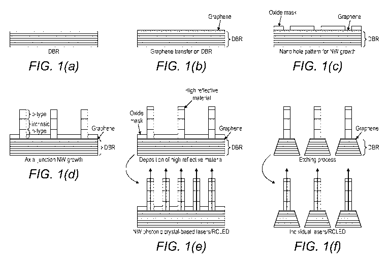
Substrate for nanowire growth
The substrate used to grow NWs is a graphitic substrate, more especially it is
graphene.
As used herein, the term graphene refers to a planar sheet of sp2-bonded
carbon atoms that are densely packed in a honeycomb (hexagonal) crystal
lattice.
This graphitic substrate should preferably be no more than 20 nm in thickness.
Ideally, it should contain no more than 10 layers of graphene or its
derivatives,
preferably no more than 5 layers (which is called as a few-layered graphene).
Especially preferably, it is a one-atom-thick planar sheet of graphene.
The crystalline or "flake" form of graphite consists of many graphene sheets
stacked together (i.e. more than 10 sheets). By graphitic substrate therefore,
is
meant one formed from one or a plurality of graphene sheets.
It is preferred if the substrate in general is 20 nm in thickness or less.
Graphene sheets stack to form graphite with an interplanar spacing of 0.335
nm.
The graphitic substrate preferred comprises only a few such layers and may
ideally
be less than 10 nm in thickness. Even more preferably, the graphitic substrate
may
be 5 nm or less in thickness. The area of the substrate in general is not
limited. This
might be as much as 0.5 mm2 or more, e.g. up to 5 mm2 or more such as up to 10
cm2. The area of the substrate is thus only limited by practicalities.
Alternatively, the graphitic substrate could be grown on a Ni film or Cu foil
by using a chemical vapour deposition (CVD) method. The substrate could be a
CVD-grown graphene substrate on metallic films or foils made of e.g. Cu, Ni,
or Pt.
These CVD-grown graphitic layers can be chemically exfoliated from the
metal foil such as a Ni or Cu film by etching or by an electrochemical
delamination
method. The graphitic layers after exfoliation are then transferred and
deposited to
the supporting carrier for NW growth. During the exfoliation and transfer, e-
beam
resist or photoresist may be used to support the thin graphene layers. These
supporting materials can be easily removed by acetone after deposition.
In some cases graphene glass may be preferred as a substrate (and
transparent spacer layer). Graphene glass is made through direct formation of
graphene over glass substrates using CVD. The use of graphene glass bypasses
CA 03051303 2019-07-23
WO 2018/141974
PCT/EP2018/052836
23
tedious and disruptive transfer procedures. By growing graphene directly on
glass
we avoid procedures where graphene is grown on metal foils and then
transferred
onto glass.
Whilst it is preferred if the graphitic substrate is used without
modification,
the surface of the graphitic substrate can be modified. For example, it can be
treated
with plasma of hydrogen, oxygen, nitrogen, NO2 or their combinations.
Oxidation
of the substrate might enhance NW nucleation. It may also be preferable to
pretreat
the substrate, for example, to ensure purity before NW growth. Treatment with
a
strong acid such as HF or BOE is an option. Substrates might be washed with
iso-
propanol, acetone, or n-methyl-2-pyrrolidone to eliminate surface impurities.
The cleaned graphitic surface can be further modified by doping. Dopant
atoms or molecules may act as a seed for growing NWs. A solution of FeCl3,
AuC13
or GaC13 could be used in a doping step.
The graphitic layers, more preferably graphene, are well known for their
superior optical, electrical, thermal and mechanical properties. They are very
thin
but very strong, light, flexible, and impermeable. Most importantly in the
present
invention they are highly electrically and thermally conducting, and
transparent.
Compared to other transparent conductors such as ITO, ZnO/Ag/ZnO, Al doped
ZnO and Ti02/Ag/TiO2 which are commercially used now, graphene has been
proven to be much more transparent (e.g. even > 92 % transmittance in the UV
spectral range from 200 to 400 nm) and conducting (< 1000 0hmo-1 sheet
resistance
for 1 nm thickness).
Support for graphitic substrate
The graphitic substrate may need to be supported in order to allow growth of
the NWs thereon. It is also important that the device contains at least one
DBR or
metal mirror in order to reflect the light (e.g. laser light) generated in the
device. In
use therefore there must be one Bragg reflector or metal mirror typically
adjacent
and parallel to the graphitic substrate on a surface opposite to the growing
NWs. As
the graphitic layer is highly transparent, the DBR or metal mirror can still
perform
its function without much loss in reflection.
CA 03051303 2019-07-23
WO 2018/141974
PCT/EP2018/052836
24
The DBR or metal mirror at the base of the device adjacent the graphitic
layer is typically designed to completely reflect light, e.g. an essentially
100% light
reflector.
A DBR or metal mirror is also preferably used at the top of the device,
parallel to the graphene layer but separated therefrom by the NWs. This
reflector
cannot be a 100% reflector as some light is emitted in the form of the laser
from the
top of the device. It will be appreciated that the DBR or metal mirrors can be
switched so that the light is emitted in either direction (but parallel to the
NWs).
If, therefore, the DBR or metal mirror can tolerate the conditions of NW
growth then conveniently, it may act as a support for the graphitic substrate
during
growth. Alternatively, the NWs are grown on supported graphene first and then
the
graphene/NWs are delaminated from the support and put on the DBR/metal mirror
afterwards.
In another embodiment, there might be a transparent spacer layer (e.g. glass
or fused silica) between the DBR and the graphitic substrate either for tuning
of
cavity length or reflectivity of the graphitic layer/spacer layer/DBR stack.
The
transparent spacer layer may act therefore as the support for the graphene. If
a
transparent spacer layer is present, there is no electrical contact between
DBR and
graphitic layer. In that situation it will be usual to employ a dielectric DBR
and use
the graphitic layer as the current injector.
Examples of preferred spacer layers include transparent layers of fused
silica,
fused quartz, fused alumina, sapphire, Si, SiC, GaAs, GaN or AN. The skilled
person will appreciate that the choice of spacer layer and its thickness may
vary
depending on the wavelength of light to be emitted by the device and the
function of
the spacer layer. Some layers may be transparent to one wavelength of light
but not
others. For example, GaAs is transparent to IR laser light. The use of
graphene
glass is preferred, where the graphene glass provides both graphitic substrate
and
spacer layer.
Preferably however the support also contains the DBR. Another advantage of
using a transparent support is that it increases the size of the cavity.
Increasing the
size of the cavity in this way may be used to change the longitudinal mode
spacing
within the cavity. If the support does not contain a reflecting layer, the
support can
CA 03051303 2019-07-23
WO 2018/141974
PCT/EP2018/052836
be provided with a reflecting layer to create, for example a three layer base
structure
of reflecting layer, support layer, graphitic layer. The support layer needs
to be inert
and transparent in this embodiment. The support may also be in the sequence
support/mirror/graphitic layer in which case the support may not be
transparent.
The term transparent is used here to mean that the support allows
transmission of light, in particular the laser light.
In theory, once the NWs are grown, the support might be removed (e.g. by
etching) or the graphitic substrate carrying the NWs can be peeled away from
the
support. It is therefore within the scope of the invention for the NWs to be
grown on
a supported graphitic layer, for the support to be removed by peeling the
graphitic
substrate with the NWs away and placed on a Bragg reflector or metal mirror in
order to prepare the device of the invention.
Nanowires
In order to prepare NWs of commercial importance, it is preferred that these
grow epitaxially on the substrate. It is also ideal if growth occurs
perpendicular to
the substrate and ideally therefore in the [0001] (for hexagonal crystal
structure)
direction or in the [111] direction (if cubic crystal structure).
The present inventors have determined that epitaxial growth on graphitic
substrates is possible by determining a possible lattice match between the
atoms in
the semiconductor NW and the carbon atoms in the graphene sheet.
The carbon-carbon bond length in graphene layers is about 0.142 nm.
Graphite has hexagonal crystal geometry. The present inventors have previously
realised that graphite can provide a substrate on which semiconductor NWs can
be
grown as the lattice mismatch between the growing NW material and the
graphitic
substrate can be very low.
The inventors have realised that due to the hexagonal symmetry of the
graphitic substrate and the hexagonal symmetry of the semiconductor atoms in
the
(111) planes of a nanowire growing in the [111] direction with a cubic crystal
structure (or in the (0001) planes of a nanowire growing in the [0001]
direction with
a hexagonal crystal structure), a lattice match can be achieved between the
growing
CA 03051303 2019-07-23
WO 2018/141974
PCT/EP2018/052836
26
nanowires and the substrate. A comprehensive explanation of the science here
can
be found in W02013/104723.
Without wishing to be limited by theory, due to the hexagonal symmetry of
the carbon atoms in graphitic layers, and the hexagonal symmetry of the atoms
in
the (111) planes of a NW growing in [111] direction with a cubic crystal
structure
(or in the (0001) planes of a NW growing in the [0001] crystal direction with
a
hexagonal crystal structure), a close lattice match between the graphitic
substrate
and semiconductor can be achieved when the semiconductor atoms are placed
above
the carbon atoms of the graphitic substrate, ideally in a hexagonal pattern.
This is a
new and surprising finding and can enable the epitaxial growth of NWs on
graphitic
substrates.
The different hexagonal arrangements of the semiconductor atoms as
described in W02013/104723, can enable semiconductor NWs of such materials to
be vertically grown to form free-standing NWs on top of a thin carbon-based
graphitic material.
Whilst it is ideal that there is no lattice mismatch between a growing NW
and the substrate, NWs can accommodate much more lattice mismatch than thin
films for example. The NWs of the invention may have a lattice mismatch of up
to
about 10% with the substrate and epitaxial growth is still possible. Ideally,
lattice
mismatches should be 7.5% or less, e.g. 5% or less.
For some semiconductors like hexagonal GaN (a = 3.189 A), hexagonal AN
(a = 3.111 A), the lattice mismatch is so small (<2%) that excellent growth of
these semiconductor NWs can be expected.
Growth of NWs can be controlled through flux ratios. The NWs grown in
the present invention may be from 250 nm to several micrometers in length,
e.g. up
to 10 micrometers. Preferably the NWs are at least 1 micrometer in length.
Where a
plurality of NWs are grown, it is preferred if they all meet these dimension
requirements. Ideally, at least 90% of the NWs grown on a substrate will be at
least
1 micrometer in length. Preferably substantially all the NWs will be at least
1
micrometer in length.
The length of the NWs is important. Ideally these are grown so that they
have a length equal to a half-integer multiple of the wavelength inside the NW
of the
CA 03051303 2019-07-23
WO 2018/141974
PCT/EP2018/052836
27
light to be emitted by the laser device. The NWs may also be grown so that the
optical cavity of each NW has a length equal to a multiple of the wavelength
of the
light to be emitted by the NW. The thickness of any spacer layer that may be
provided may be taken into account to provide an optical cavity of desired
length.
Moreover, it will be preferred if the NWs grown have the same dimensions,
e.g. to within 10% of each other. Thus, at least 90% (preferably substantially
all) of
the NWs on a substrate will preferably be of the same diameter and/or the same
length (i.e. to within 10% of the diameter/length of each other). Essentially,
therefore the skilled man is looking for homogeneity and NWs that are
substantially
the same in terms of dimensions.
The length of the NWs is often controlled by the length of time for which the
growing process runs. A longer process typically leads to a (much) longer NW.
The NWs have typically a hexagonal cross sectional shape. The NW may
have a cross sectional diameter of 25 nm to several hundred nm (i.e. its
thickness),
e.g. 300 nm. As noted above, the diameter is ideally constant throughout the
majority of the NW. NW diameter can be controlled by the manipulation of the
ratio of the atoms used to make the NW as described further below.
Moreover, the length and diameter of the NWs can be affected by the
temperature at which they are formed. Higher temperatures encourage high
aspect
ratios (i.e. longer and/or thinner NWs). The diameter can also be controlled
by
manipulating the nanohole opening size of the mask layer. The skilled man is
able to
manipulate the growing process to design NWs of desired dimensions.
The NWs of the invention are formed from at least one III-V compound
semi-conductor. Preferably, the NWs consist of group III-V compounds grown as
discussed below to generate a light generating region in each NW. Preferably,
the
light generating regions each comprise a heterostructure. There will be more
than
one different group III-V compound present but it is preferred if all
compounds
present are group III-V compounds.
Group III element options are B, Al, Ga, In, and Tl. Preferred options here
are Ga, Al and In.
Group V options are N, P, As, Sb. All are preferred, especially N.
CA 03051303 2019-07-23
WO 2018/141974
PCT/EP2018/052836
28
It is of course possible to use more than one element from group III and/or
more than one element from group V. Preferred compounds for NW manufacture
include AlAs, GaSb, GaP, GaN, AN, AlGaN, InGaN, AlGaInN, GaAs, GaAsSb,
InP, InN, InGaAs, InSb, InAs, or AlGaAs. Compounds based on Al, Ga and In in
combination with N are most preferred. The use of GaN, AlGaN, InGaN, AlInGaN
or AN is highly preferred.
It is most preferred if the NWs consist of Ga, Al, In and N (along with any
doping atoms as discussed below).
Whilst the use of binary materials is possible, the use of ternary NWs in
which there are two group III cations with a group V anion are preferred here,
such
as AlGaN. The ternary compounds may therefore be of formula XYZ wherein X is
a group III element, Y is a group III different from X, and Z is a group V
element.
The X to Y molar ratio in XYZ is preferably 0.1 to 0.9, i.e. the formula is
preferably
XxYiõZ where subscript xis 0.1 to 0.9.
Quaternary systems might also be used and may be represented by the
formula AxBi,CyDi_y where A and B are different group III elements and C and D
are different group V elements. Again subscripts x and y are typically 0.1 to
0.9.
Other options will be clear to the skilled man.
The growth of GaAs, InGaN, AlGaN and AlInGaN NWs is especially
preferred. The wavelength of light emitted by a device containing these NWs
can be
tailored by manipulating the content of Al, In and Ga. Alternatively, the
pitch
and/or diameter of the NWs can be varied to change the nature of the light
emitted.
Doping
The NWs of the invention comprise a light generating region (i.e. gain
medium). Each gain medium can be used to generate light. When the NWs are
arranged in an array, they may be optically coupled to generate light. As
such, the
NWs ideally need to comprise at least one heterostructure such as at least one
lower
bandgap section/insert, quantum well, quantum dot or superlattice. It is
highly
preferred if the intrinsic region of the p-i-n junction comprises at least one
quantum
well, quantum dot or superlattice. Devices of the invention are therefore
preferably
CA 03051303 2019-07-23
WO 2018/141974
PCT/EP2018/052836
29
provided with an undoped intrinsic semiconductor region between a p-type
semiconductor and an n-type semiconductor region.
The NWs may be optically pumped or electrically pumped to excite/inject
carriers within the light generating region.
In an optically pumped device, an intrinsic region may comprise a
heterostructured active gain medium. Often the gain medium may contain 10 or
more, such as 20 or more periods of heterostructured active gain medium, e.g.
with a
thickness of 100 nm for each segment. After the growth of the active gain
medium, a
passivation layer (e.g. a shell layer) may be added to passivate the surface
of the
light generating region and/or each heterostructure for enhanced light
generation.
It will be appreciated that an optically pumped device does not need to
comprise doping ¨ e.g. it does not need to comprise an n-type doped and a p-
type
doped region.
In an electrically pumped device, the provision of n-type doped and p-type
doped regions enables carriers (i.e. electrons and/or holes) to be injected
more
efficiency into the light generating region (e.g. intrinsic region which may
comprise
a quantum heterostructure). Injected carriers, and/or excited carriers, within
the light
generating region may recombine (e.g. an electron-hole pair may recombine) to
generate light, as mentioned previously. Due to the quantum carrier
confinement
effects found in quantum heterostructures, quantum heterostructures exhibit
more
efficient carrier recombination than bulk material such as bulk intrinsic
materials.
Bulk materials typically considered to have continuous energy level. In
contrast,
quantum heterostructures typically have at least one discrete energy state.
Doping typically involves the introduction of impurity ions into the NW, e.g.
during MBE or MOVPE growth. The doping level can be controlled from ¨
1015/cm3to 1020/cm3. The NWs can be doped to provide p-type doped regions
and/or
n-type doped regions as desired. Doped semiconductors are extrinsic
conductors.
The n(p)-type semiconductors/regions have a larger electron (hole)
concentration than hole (electron) concentration by doping an intrinsic
semiconductor with donor (acceptor) impurities. Suitable donor (acceptors) for
III-V
compounds can be Si (Mg, Be or Zn). Dopants can be introduced during the
growth
process or by ion implantation of the NWs after their formation.
CA 03051303 2019-07-23
WO 2018/141974
PCT/EP2018/052836
In order to create quantum dots, quantum wells or superlattice structures
within the NWs, it is generally required to form very thin semiconductor
layers,
often only several nanometres in size, within the NW bulk. The layers are so
thin
that their optical and electronic properties differ from those of thicker
layers.
Thus, where a quantum heterostructure is present, the NWs of the invention
are not formed from a single group III-V material. They are heterostructured
and
therefore comprise at least two different semiconductor compounds. By
inserting
thin layers of a secondary group III-V semiconductor into the bulk material
composition of the NW (which preferably has a higher bandgap than the low
bandgap region of the quantum heterostructures), we may create a NW with a
quantum heterostructure for generating light.
In order to provide quantum confinement, the low bandgap regions (e.g.
layers) of the quantum heterostructures typically need to have a size on the
order of
the de Broglie wavelength, as discussed previously. For example, a low bandgap
layer of a quantum well heterostructure may be grown to have thickness of a
few nm
thick (such as 1 to 20 nm) so that the energy levels in the low bandgap layer
become
quantized. Quantum wells have quantum confinement in only one spatial
dimension,
whereas quantum dots have quantum confinement in all three spatial dimensions.
A
superlattice (i.e. a semiconductor superlattice) is a periodic structure of
quantum
confined structures (quantum wells or quantum dots) where the barrier layers
are
thin enough (typically a few nanometers) to allow carrier transport by
tunnelling to
take place between the quantum wells/quantum dots. Short-period superlattices
can
also be applied for bandgap tailoring purposes, grading the bandgap by
increasing
(decreasing) the barrier-layer thickness and decreasing (increasing) the well-
layer
thickness along the growth direction to increase (decrease) the bandgap
experienced
by the charge carriers. Such grading superlattices can e.g. be used between
lower
bandgap material sections and higher bandgap material sections in the doped
regions
to improve majority carrier transport properties between the two materials of
different bandgap.
A quantum dot might be formed using a thin GaAsSb layer as the low
bandgap region and GaAs layers as the high bandgap region (thus, in this case,
GaAs layers act as barrier regions). The NWs of the invention can be grown to
CA 03051303 2019-07-23
WO 2018/141974
PCT/EP2018/052836
31
have a heterostructured form radially or axially. For example, for an axial
heterostructured NW, p-n junction can be axially formed by growing a p-type
doped
core first, and then continue with an n-type doped core (or vice versa). An
intrinsic
region can be positioned between doped cores for a p-i-n NW. Heterostructures
or
quantum heterostructures can be introduced into the intrinsic region by
varying the
elements fed during the growing process. For a radially heterostructured NW, p-
i-n
junction can be radially formed by growing the p-type doped NW core first,
then an
intrinsic shell and then the n-type doped semiconducting shell is grown (or
vice
versa). Quantum heterostructures can be introduced into the intrinsic region
by
varying the elements fed during the growing process.
In a p-i-n NW, when charge carriers are injected into the respective p- and n-
regions, they recombine in the i-region, and this recombination generate
light, as
previously discussed.
In a preferred embodiment for providing UV light (e.g. laser light), the NW
may comprise a p-i-n structure. The i-region could consist of
AlxGai_xN/AlyGaii,N
(x > y) multiple quantum wells/quantum dots or a superlattice structure. The p-
region could include/comprise an electron blocking layer (single or multiple
barriers
in the conduction band) to prevent the overflow of minority carriers
(electrons) into
the p-region. The n-region could include/comprise a hole blocking layer
(single or
multiple barriers in the valence band) to prevent the overflow of minority
carriers
(holes) into the n-region.
It is thus a preferred embodiment if the NW is provided with a quantum
heterostructure (e.g. multiple quantum wells/quantum dots/superlattices). It
is thus a
preferred embodiment if the NW is provided with an electron blocking layer
or/and
a hole blocking layer.
Growth
The NWs of the invention preferably grow epitaxially. They attach to the
underlying substrate through covalent, ionic or quasi van der Waals binding.
Accordingly, at the junction of the substrate and the base of the NW, crystal
planes
are formed epitaxially within the NW. These build up, one upon another, in the
same
crystallographic direction thus allowing the epitaxial growth of the NW.
Preferably
CA 03051303 2019-07-23
WO 2018/141974
PCT/EP2018/052836
32
the NWs grow vertically. The term vertically here is used to imply that the
NWs
grow perpendicular to the substrate. It will be appreciated that in
experimental
science the growth angle may not be exactly 90 but the term vertically
implies that
the NWs are within about 10 of vertical/perpendicular, e.g. within 5 .
Because of
the epitaxial growth via covalent, ionic or quasi van der Waals bonding, it is
expected that there will be an intimate contact between the NWs and the
graphitic
substrate. To enhance the contact property further, the graphitic substrate
can be
doped to match the major carriers of grown NWs.
Because NWs are epitaxially grown involving physical and chemical
bonding to substrates at high temperature, the bottom contact is preferably
ohmic.
It will be appreciated that the substrate comprises one or more NWs, but
preferably a plurality of NWs. Preferably the NWs grow about parallel to each
other. It is preferred therefore if at least 90%, e.g. at least 95%,
preferably
substantially all NWs grow in the same direction from the same plane of the
substrate.
Ideally the grown NWs are substantially parallel. Preferably, the NWs grow
substantially perpendicular to the substrate.
The NWs of the invention should preferably grow in the [0001] or [111]
direction for NWs with hexagonal or cubic crystal structures respectively. If
the NW
has a hexagonal (cubic) crystal structure, then the (0001) [111] interface
between the
NW and the graphitic substrate represents the surface from which axial growth
takes
place. The NWs are preferably grown by MBE or MOVPE. In the MBE method,
the substrate is provided with a molecular beam of each reactant, e.g. a group
III
element and a group V element preferably supplied simultaneously. A higher
degree
of control of the nucleation and growth of the NWs on the graphitic substrate
might
be achieved with the MBE technique by using migration-enhanced epitaxy (MEE)
or atomic-layer MBE (ALMBE) where e.g. the group III and V elements can be
supplied alternatively.
A preferred technique in case of nitrides is plasma assisted solid-source
MBE, in which very pure elements such as gallium, aluminium, and indium are
heated in separate effusion cells, until they begin to slowly evaporate. The
rf-plasma
nitrogen source is typically used to produce low energy beams of nitrogen
atoms.
CA 03051303 2019-07-23
WO 2018/141974
PCT/EP2018/052836
33
The gaseous elements then condense on the substrate, where they may react with
each other. In the example of gallium and nitrogen, single-crystal GaN is
formed.
The use of the term "beam" implies that evaporated atoms (e.g. gallium) and
nitrogen atoms from the plasma source do not interact with each other or
vacuum
chamber gases until they reach the substrate.
MBE takes place in ultra-high vacuum, with a background pressure of
typically around 10-10 to 10-9 Torr. This allows NWs to grow epitaxially and
maximises structural performance.
The nature of the light emitted is a function of the dimensions and geometry
of the quantum hetero structures in the active region of the NW. In order to
tune the
various bandgaps in the quantum heterostructures in the NW, temperature and
fluxes
can be used. (Nanotechnology 25 (2014) 455201).
In the MOVPE method, the substrate is kept in a reactor in which the
substrate is provided with a carrier gas and a metal organic gas of each
reactant, e.g.
a metal organic precursor containing a group III element and a metal organic
precursor containing a group V element. The typical carrier gases are
hydrogen,
nitrogen, or a mixture of the two. A higher degree of control of the
nucleation and
growth of the NWs on the graphitic substrate might be achieved with the MOVPE
technique by using pulsed layer growth technique, where e.g. the group III and
V
elements can be supplied alternatively.
Positioned growth of nanowires
The NWs of the invention are preferably grown positioned. This method
may require a mask with nano-hole patterns deposited on the graphitic layers.
In order to prepare a more regular array of NWs with better homogeneity in
height and diameter of grown NWs, the inventors envisage the use of a mask on
the
substrate. This mask can be provided with regular holes, where NWs can grow
homogeneously in size in a regular array across the substrate. The hole
patterns in
the mask can be easily fabricated using conventional photo/e-beam lithography
or
nanoimprinting. Focussed ion beam technology may also be used in order to
create
a regular array of nucleation sites on the graphitic surface for the NW
growth.
CA 03051303 2019-07-23
WO 2018/141974
PCT/EP2018/052836
34
Thus a mask can be applied to the substrate and etched with holes exposing
the substrate surface, optionally in a regular pattern. Moreover, the size and
the
pitch of the holes can be carefully controlled. By arranging the holes
regularly, a
regular pattern of NWs can be grown.
Moreover, the size of the holes can be controlled to ensure that only one NW
can grow in each hole. Finally, the holes can be made of a size where the hole
is
sufficiently large to allow NW growth. In this way, a regular array of NWs can
be
grown.
By varying the size of the holes, one could control the size of the NW. It is
important that the holes are suitably spaced. If the holes and hence the
growing
NWs are spaced by less than the wavelength of the light emitted by the laser
then the
NW array may act as a photonic crystal (PC). An array of 75 to 150 by 75 to
150
NWs, e.g. 100 x 100 NWs is a possible size. It should be noted that these
numbers
could vary massively depending on the design of the device.
The mask material can be any material which does not damage the
underlying substrate when deposited. The mask may also be transparent to the
laser
light. The minimum hole size might be 50 nm, preferably at least 100-200 nm.
The
thickness of the mask can be 10 to 100 nm, such as 10 to 40 nm.
The mask itself can be made of an inert compound, such as silicon dioxide or
silicon nitride. In particular, the hole-patterned mask comprises at least one
insulating material such as SiO2, Si3N4, Hf02, TiO2 or A1203 e.g. deposited by
e-
beam evaporation, CVD, plasma enhanced-CVD (PE-CVD), sputtering, or atomic
layer deposition (ALD). The mask can therefore be provided on the substrate
surface by any convenient technique such as by electron beam deposition, CVD,
PE-
CVD, sputtering, and ALD .
The use of a Ti mask that is either nitridated/oxidized before the NW growth,
is particularly preferred as such a mask has been found to allow growth of
uniform
NWs (e.g. see J. Crystal Growth 311(2009) 2063-68).
Positioned growth using hole-patterned masks yields NWs of uniform length
and diameter at predefined positions. The NWs can also be grown without mask
with nano-hole patterns. In such case, the NWs will have non-uniform sizes
(length
and diameter), and located at random positions. In one embodiment, it is
preferred
CA 03051303 2019-07-23
WO 2018/141974
PCT/EP2018/052836
if no mask is used to grow the NWs of the invention. Moreover, the present
inventors have found that NW density can be maximised in the absence of a
mask.
NW densities of at least 20 NWs per square micrometer are possible, such as at
least
25 NWs per square micrometer. These very high NW densities are particularly
associated with GaN, InGaN or AlGaN NWs.
For the NW growth, the graphitic substrate temperature can then be set to a
temperature suitable for the growth of the NW in question. The growth
temperature
may be in the range 300 to 1200 C. The temperature employed is, however,
specific
to the nature of the material in the NW and the growth method. For GaN grown
by
MBE, a preferred temperature is 700 to 950 C, e.g. 750 to 900 C, such as 760
C.
For AlGaN the range is slightly higher, for example 800 to 1100 C, such as 830
to
950 C, e.g. 840 C.
It will be appreciated therefore that the NWs can comprise different group
III-V semiconductors within the NW, e.g. starting with a GaN stem followed by
an
AlGaN component or AlGaInN component and so on.
GaN NW growth in MBE can be initiated by opening the shutter of the Ga
effusion cell, the nitrogen plasma cell, and the dopant cell simultaneously
initiating
the growth of doped GaN NWs, hereby called as stem. The length of the GaN stem
can be kept between 5 nm to several 100s of nanometers. Subsequently, one
could
increase the substrate temperature if needed, and open the Al shutter to
initiate the
growth of AlGaN NWs. One could initiate the growth of AlGaN NWs on graphitic
layers without the growth of GaN stem. n- and p-type doped NWs can be obtained
by opening the shutter of the n-type dopant cell and p-type dopant cell,
respectively,
during the NW growth. For example, Si dopant cell for n-type doping of NWs,
and
Mg dopant cell for p-type doping of NWs.
This process can be adapted to the growth of other group III-V NWs with
suitable doping.
The temperature of the effusion cells can be used to control growth rate.
Convenient growth rates, as measured during conventional planar (layer by
layer)
growth, are 0.05 to 2 pm per hour, e.g. 0.5 pm per hour. The pressure of the
molecular beams can also be adjusted depending on the nature of the NW being
CA 03051303 2019-07-23
WO 2018/141974
PCT/EP2018/052836
36
grown. Suitable levels for beam equivalent pressures are between 1 x 10⁻⁷ and
1 x
10-4 Torr.
The beam flux ratio between reactants (e.g. group III atoms and group V
molecules) can be varied, the preferred flux ratio being dependent on other
growth
parameters and on the nature of the NW being grown. In the case of nitrides,
III-
nitride NWs are always grown under nitrogen rich conditions.
It is thus an embodiment of the invention to employ a multistep, such as two
step growth procedure, e.g. to separately optimize the NW nucleation and NW
growth.
A significant benefit of MBE is that the growing NW can be analysed in situ,
for instance by using reflection high-energy electron diffraction (RHEED).
RHEED
is a technique typically used to characterize the surface of crystalline
materials. This
technology cannot be applied so readily where NWs are formed by other
techniques
such as MOVPE.
A significant benefit of MOVPE is that the NWs can be grown at a much
faster growth rate. This method favours the growth of radial heterostructure
NWs
and microwires, for example: n-type doped GaN core with shell consisting of
intrinsic A1N/A1(In)GaN multiple quantum wells (MQW), AlGaN electron blocking
layer (EBL), and p-type doped (A1)GaN shell. This method also allows the
growth
of axial heterostructured NW using techniques such as pulsed growth technique
or
continuous growth mode with modified growth parameters for e.g., lower V/III
molar ratio and higher substrate temperature.
In more detail, the reactor must be evacuated after placing the sample, and is
purged with N2 to remove oxygen and water in the reactor. This is to avoid any
damage to the graphene at the growth temperatures, and to avoid unwanted
reactions
of oxygen and water with the precursors. The total pressure is set to be
between 50
and 400 Torr. After purging the reactor with N2, the substrate is thermally
cleaned
under H2 atmosphere at a substrate temperature of about 1200 C. The substrate
temperature can then be set to a temperature suitable for the growth of the NW
in
question. The growth temperature may be in the range 700 to 1200 C. The
temperature employed is, however, specific to the nature of the material in
the NW.
For GaN, a preferred temperature is 800 to 1150 C, e.g. 900 to 1100 C, such
as
CA 03051303 2019-07-23
WO 2018/141974
PCT/EP2018/052836
37
1100 C. For AlGaN the range is slightly higher, for example 900 to 1250 C,
such as
1050 to 1250 C, e.g. 1250 C.
The metal organic precursors can be either trimethylgallium (TMGa) or
triethylgallium (TEGa) for Ga, trimethylalumnium (TMA1) or triethylalumnium
(TEA1) for Al, and trimethylindium (TMIn) or triethylindium (TEIn) for In. The
precursors for dopants can be SiH4 for silicon and
bis(cyclopentadienyl)magnesium
(Cp2Mg) or bis(methylcyclopentadienyl)magnesium ((MeCp)2Mg) for Mg. The flow
rate of TMGa, TMA1 and TMIn can be maintained between 5 and 100 sccm. The
NH3 flow rate can be varied between 5 and 150 sccm.
In particular, the simple use of vapour-solid growth may enable NW growth.
Thus, in the context of MBE, simple application of the reactants, e.g. In and
N, to
the substrate without any catalyst can result in the formation of a NW. This
forms a
further aspect of the invention which therefore provides the direct growth of
a
semiconductor NW formed from the elements described above on a graphitic
substrate. The term direct implies therefore the absence of a catalyst to
enable
growth.
Said regions can be represented by layers within a NW or shells on a core to
create the NW. Thus, the invention further provides a plurality of radial
group III-V
NWs grown epitaxially on a graphitic substrate comprising, in this order, an n-
type
doped core with shell comprising an intrinsic multiple quantum well/quantum
dot/superlattice, an electron blocking layer (EBL), and p-type doped shell.
The n-
type doped region could include/comprise a hole blocking layer (single or
multiple
barriers in the valence band) to prevent the overflow of minority charge
carriers
(holes) into the n-type doped region.
Distributed Bragg Reflector or metal mirror
The laser device of the invention comprises at least one, preferably two
distributed Bragg reflectors (DBRs) or metal mirrors. The DBRs or metal
mirrors
define the resonant cavity (the NWs) and the device is defined by a highly
reflective
DBR mirror or metal mirror at one end, preferably a lower reflectivity DBR or
metal
CA 03051303 2019-07-23
WO 2018/141974
PCT/EP2018/052836
38
mirror on the other end of the NWs. Ideally, the higher reflectivity DBR or
metal
mirror is positioned adjacent the graphitic layer.
Within the cavity, the NWs comprise a gain medium, where current is
injected to produce light ¨ e.g. laser light having a single spatial lasing
mode. The
DBR is designed to reflect only in a single longitudinal mode. As a result,
the laser
operates on a single spatial and longitudinal mode. The laser preferably emits
from
the exit facet opposite the highly reflective DBR or metal mirror.
DBRs are tunable over approximately a 2 nm range by changing current or
temperature.
The DBR preferably comprises alternating layers of semiconductors that
have different refractive indices. Each layer preferably has a thickness of a
quarter
of the laser wavelength in the material, yielding intensity reflectivities
above 99%
for the DBR. The semiconductors used are ideally group III-V semiconductors.
Different refractive indexes can be achieved by varying the group III or group
V
atoms present in each layer.
The distributed Bragg reflector preferably comprises a plurality of
semiconductor layers, preferably group III-V semiconductor layers. The
semiconductor DBR must have 2 different group III-V semiconductors, e.g. GaAs
and AlAs.
Adjacent layers have a different refractive index. Typically each DBR might
contain 8 to 40 layers, such as 10 to 35 layers. Each layer may be 5 to 200 nm
in
thickness, such as 10 to 100 nm in thickness. Layers ideally reflect the
refractive
index of the layer in question. Thus, each layer might be 250 nm/refractive
index of
the layer. As typical refractive indices are around 3-4, the layer thickness
may be 60
nm or so.
A preferred distributed Bragg reflector for a GaAsSb laser comprises
alternate layers of GaAs and Al(Ga)As. The DBR may comprise a plurality of
GaAs layers positioned between two AlAs layers. The distributed Bragg
reflectors
must reflect and not absorb light and hence their bandgap should be higher
than that
equivalent to the wavelength of light generated in the NW.
The DBR has to be tuned to the light from the NW ¨ e.g. laser light
generated in the NW. As the light is reflecting up and down the NW, the
intensity is
CA 03051303 2019-07-23
WO 2018/141974
PCT/EP2018/052836
39
amplified. Once lasing threshold is achieved, coherent emission of light is
released.
Each NW will lase with a particular wavelength.
In common VCSELs, the upper and lower DBRs are doped as p-type and n-
type materials, forming a diode junction. It will also be preferred if the
distributed
Bragg reflectors in this case are doped. The doping materials used can be
those
discussed above in connection with the NWs.
The DBR may also be dielectric. The DBR may comprise alternating layers
of dielectric materials that have different refractive indices. The dielectric
Bragg
pairs could be e.g. TiO2 (refractive index around 2.5) and silica (refractive
index
around 1.5). Other common materials in dielectric DBRs are magnesium fluoride,
tantalum pentoxide (n = 2.275) and zinc sulphide (n = 2.32). The melting
temperatures of typical dielectric materials used in DBRs are high.
As an alternative to a distributed Bragg reflector at the bottom and/or top of
the device, a metallic reflective layer might be used, e.g. based on Al. High
reflectivity mirrors are required in VCSELs to balance the short axial length
of the
gain medium.
Such a metallic layer may comprise aluminium, gold, silver, chromium, or
rhodium. Preferably, the reflector is arranged to feedback light emerging from
the
NW back into the NW.
In one embodiment it may be possible to grow a distributed Bragg reflector
within the actual NW itself.
In one embodiment, it is possible to etch the graphitic layer and distributed
Bragg reflector to create islands of NWs or individual NWs on a base
structure.
Filler
It is within the scope of the invention to use a filler to surround the
assembly
where the filler may be transparent to the emitting light. Filler may be
present in the
space between NWs and/or around the assembly as a whole. Different fillers
might
be used in the spaces between the NWs than in the assembly as a whole. The
filler
may comprise a semiconductor material having a higher bandgap than the
materials
of the NW. Alternatively the filler may comprise a polymer and/or a resin.
CA 03051303 2019-07-23
WO 2018/141974
PCT/EP2018/052836
Device
The device of the invention might contain an array of 100 by 100 NWs. A
dense array of NWs should enhance the power of the device. The NW array pitch
may be tuned to act as a photonic crystal (PC) for enhanced performance. The
NW
diameter is ideally designed to confine a single optical mode, preferably the
fundamental mode. It may emit in the UV, IR or visible spectrum, especially
UV.
VCSELs in general have many applications, the most important of which are
briefly discussed in the following.
Due to the short resonator round-trip time, VCSELs can be modulated with
frequencies well in the gigahertz range. This makes them useful as
transmitters for
optical communications. Some VCSELs are used in laser computer mice since a
VCSEL as light source can have a high tracking precision combined with a low
electricity consumption.
Another prominent field of application is gas sensing with wavelength-
tunable VCSELs. VCSELs can also be used in miniature optical clocks, where the
laser beam probes an atomic transition in cesium vapor. Such clocks could
become
part of compact GPS devices.
Whilst the invention is described with reference to vertical cavity lasers, it
is
envisaged that the same device could be adapted for use as a RCLED. The device
will act as an RCLED if the excitation level is below the lasing threshold. In
an
RCLED, spontaneous emission is generated in a multilayer Fabry¨Perot (FP)
resonator, in which interference effects alter the internal angular power
distribution.
In these devices, the active layer is embedded in a cavity with at least one
dimension of the order of the wavelength of the emitted light. Under those
circumstances, the spontaneous emission process itself is modified, such that
the
internal emission is no longer isotropic.
Brief Description of the Figures
CA 03051303 2019-07-23
WO 2018/141974
PCT/EP2018/052836
41
Fig. 1 summarizes the fabrication process of an integrated
NW/graphene/DBR laser or RCLED device. Due to the coherent coupling among
DBR, NWs, and high reflectivity NW top-mirror, a NW-based vertical-cavity
surface-emitting laser (VCSEL) will be demonstrated with the ultimate goal of
achieving low threshold current and high light emission efficiency. Surface-
emitting
PC properties can also be developed by tuning the NW diameter and the pitch
size
between the NWs. The DBR can be made of multilayers of thin films grown by
MBE (e.g. GaAs/AlAs), where crystal orientation is in general (100). Another
type
of DBR can be fabricated with insulating layers. However, such thin films with
crystal orientation of (100) or insulating layers cannot be used for vertical
NW
growth. This issue can be solved by using graphene as a buffer layer. In
addition, the
graphene can be used as a carrier injection layer due to its high conductivity
and
transparency.
In figure 1(a) a DBR is provided onto which is placed a graphene layer
(figure b). Subsequently mask layer can be applied and etched to form holes
for
positioned NW growth (figure c).
NWs are grown in the holes such that an n-type doped region is made first
followed by the i-region and p-type doped region (figure d). A top reflective
layer
can then be applied such as an Al metal layer (i.e. a metal mirror). The
intrinsic
region may comprise a series of quantum heterostructures (e.g. quantum
wells/quantum dots or a superlattice).
Optionally, the graphene layer and Bragg reflector can be etched to create
individual NW lasers (f).
Both electrically and optically pumped NW lasers are designed with axial
(Fig. 2 (a,b)) or radial heterostructures (Fig. 2(c)) of lower and higher
bandgap
materials to enhance the gain for lasing. A self-catalyzed vapor-liquid-solid
method
will be used to grow GaAs-based NW lasers on graphene, for example GaAs with
InGaAs inserts/wells or GaAsSb inserts/wells, and the catalyst-free method
will be
used for the growth of III-N-based NW lasers on graphene, for example AlGaN
NWs with GaN inserts/wells or InGaN inserts/wells. Furthermore, a high-quality
DBR, for example with AlAs/GaAs or AlN/GaN Bragg pairs, will be grown by
CA 03051303 2019-07-23
WO 2018/141974
PCT/EP2018/052836
42
MBE or MOCVD, onto which graphene (e.g. single-layer or double-layer) will be
transferred for subsequent growth of the NW laser or RCLED.
Fig. 3 describes a structure and laser spectra of a single GaAsSb/GaAs
heterostructured NW laser. The NW laser consists of periodic segments of
GaAsSb
and GaAs. By optical pumping, the NW lases in the near-IR and causes an
interference pattern as shown in Fig. 3(b). By tuning the composition and
structure,
the GaAsSb/GaAs heterostructured NW laser can lase covering a wide range of
wavelengths as shown in Fig. 3(c).
In figure 4(a), a bottom DBR or metal mirror is provided with a transparent
intermediate layer such as a silica layer on top of which is located the
graphene
layer. This arrangement allows for tuning of reflectivity and/or protection
(capping)
of e.g. GaAs/Al(Ga)As DBR during further epitaxial growth (at high
temperature) of
NWs on the graphene.
In figure 4(b), the DBR is located at the top of the NWs with a transparent
silica, e.g. fused silica, support or other transparent support being used to
carry the
graphene layer. Optionally graphene glass may be used as combined substrate
and
support.
Figure 4(c) shows an alternative option to the structure displayed in figure
4(a), where the graphene and the transparent intermediate layer are replaced
by
graphene glass which can also provide support during NW growth. Bottom DBR or
metal mirror can be provided after NW growth.
In figure 4(d), the glass supports the DBR.
Fig. 5(a) presents the schematic of a grown NW/graphene/DBR structure .
Before the NW growth, exfoliated graphene flakes were placed on top of the DBR
reflector, as depicted in the optical image of fig. 5(b). Fig. 5(c) shows a 30
tilted
SEM image of a 7 um long GaAsSb-based superlattice NW epitaxially grown
perpendicular on the tiny graphene flake circled in red and marked as C in
fig. 5(b).
The measured normalized reflectivity of the GaAs/AlAs DBR structure is shown
as
the blue curve in fig. 5(d), which contains a high reflectivity plateau around
890 to
990 nm and reflectance fringes outside the plateau. By exerting optical
excitation,
photoluminescence is observed from the GaAsSb-based superlattice NW with
Fabry-Perot modes, which is marked by vertical red dashed lines. The spacing
CA 03051303 2019-07-23
WO 2018/141974
PCT/EP2018/052836
43
among the Fabry-Perot modes is around 11.6 nm, which corresponds to an energy
spacing of 6E= 16 meV around 950 nm. This correlates well to the theoretical
value
of 16.7 meV found for the expected TE01 mode using ngroup=5.35 found from
calculations based on FDTD simulations.
The NW is grown in the [111] crystal direction, and perpendicular to the
graphitic surface, whereas the GaAs/AlAs DBR (thin film) is grown in the [001]
crystal direction on an n-type GaAs(001) wafer.
Example 1
Electrically pumped AlN/AlGaN/GaN axial heterostructured NW lasers
(RCLEDs) on graphene/DBR:
GaN-based NWs with AlN/AlGaN axial quantum heterostructured active
gain medium are grown on a dielectric DBR (e.g. a DBR with SiO2 (n=1.5) and
TiO2 (n=2.5) Bragg pairs) with graphene buffer. The heavily n-doped GaN NW
segment is epitaxially grown directly on the graphene/DBR structure, which is
followed by the growth of a heavily n-doped AN segment, 5 periods of intrinsic
AlN/AlGaN quantum heterostructured active gain medium, and a p-doped MN
segment. After that, a p-doped GaN top segment is grown for top contact.
Example 2
Optically pumped GaAsSb/GaAs axial heterostructured NW lasers on
graphene/DBR:
Intrinsic GaAs with GaAsSb/GaAs axial quantum heterostructured active
gain medium are grown on a GaAs/AlAs DBR using a graphene buffer. After
nucleation by using AlAsSb buffer as nucleation stem, GaAs NWs are directly
epitaxially grown on the graphene/DBR structure, which is followed by the
growth
of 60 periods of intrinsic GaAsSb/GaAs quantum heterostructured active gain
medium with a thickness of 100 nm for each segment. After the growth of the
active
gain medium, an AlGaAs shell with thickness of 15 nm is grown to passivate the
surface for enhanced light performance.
CA 03051303 2019-07-23
WO 2018/141974
PCT/EP2018/052836
44
Example 3
NW/graphene/DBR RCLED.
Before the NW growth, exfoliated graphene flakes were placed on top of a
GaAs/AlAs DBR reflector. The GaAs/AlAs DBR (thin film) is grown in the [001]
crystal direction on an n-type GaAs(001) wafer. The measured normalized
reflectivity of the GaAs/AlAs DBR structure is shown inig. 5(d). It contains a
high
reflectivity plateau around 890 to 990 nm and reflectance fringes outside the
plateau.
71..tm long GaAsSb-based superlattice NWs were epitaxially grown
perpendicular on the graphene/DBR structure in the [111] crystal direction.
By exerting optical excitation, photoluminescence is observed from the
GaAsSb-based superlattice NW with Fabry-Perot modes, which is marked by
vertical red dashed lines. The spacing among the Fabry-Perot modes is around
11.6
nm, which corresponds to an energy spacing of 6E= 16 meV around 950 nm. This
correlates well to the theoretical value of 16.7 meV found for the expected
TE01
mode using ngroup=5.35 found from calculations based on FDTD simulations.