Note: Descriptions are shown in the official language in which they were submitted.
CA 03051312 2019-07-23
WO 2018/149733 PCT/EP2018/053192
1
CONNECTOR FOR PRINTED CIRCUIT BOARDS
The present invention relates to a connector for printed circuit boards.
Electrical connectors and terminal strips are known which allow to
electrically connect printed circuit boards, also known as PCBs, to electrical
cables in order to supply power to the devices that are present on the circuit
itself
Among the various types of connector, those with a screw tightening
system are known.
These connectors are constituted typically by an enclosure made of
insulating material with a plurality of cavities that can be accessed from the
outside so that each accommodates an electrical cable. The enclosure is also
provided with openings through which the connection to the connector
elements of the printed circuit board is created.
At right angles to each cavity there is a screw which, when screwed
toward the inside of the enclosure, presses the inserted electrical cable
against a component that carries the electrical connection to the connector
elements of the board.
These connectors, despite being widespread and allowing wiring of
cables with a cross-section up to 1.5 mm2, have a significant drawback,
which is due to the vertical space occupation, which is greater than 11 mm.
With technological progress, the trend is to miniaturize electrical
devices and render them more compact, but currently commercially
available connectors set a limit to this miniaturization.
The aim of the present invention is to provide a connector for printed
circuit boards that is capable of improving the background art in one or
more of the aspects indicated above.
Within this aim, an object of the invention is to propose a connector
that has smaller dimensions than those currently commercially available.
Another object of the invention is to propose a connector by virtue of
which to reduce the overall space occupation of the printed circuit boards on
CA 03051312 2019-07-23
WO 2018/149733 PCT/EP2018/053192
2
which the connector is installed.
Furthermore, an object of the present invention is to overcome the
limitations of the background art in a manner that is alternative to any
existing solutions.
A still further object of the invention is to provide a connector that is
highly reliable, relatively easy to provide and at competitive costs.
This aim, as well as these and other objects which will become better
apparent hereinafter, are achieved by a connector according to claim 1,
optionally provided with one or more of the characteristics of the dependent
claims.
Further characteristics and advantages of the invention will become
better apparent from the description of a preferred but not exclusive
embodiment of the connector according to the invention, illustrated by way
of nonlimiting example in the accompanying drawings, wherein:
Figure 1 is a top view of the connector according to the invention;
Figure 2 is a side view of the connector according to the invention;
Figure 3 is a cross-sectional view of the connector according to the
invention in an inactive configuration;
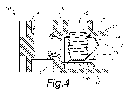
Figure 4 is a cross-sectional view of the connector according to the
invention, similar to Figure 3, in the active configuration.
With reference to the cited figures, the connector according to the
invention, designated generally by the reference numeral 10, comprises an
enclosure 11 made of insulating material with at least one cavity 12 that can
be accessed from the outside in order to accommodate at least one electrical
cable 13 and means 14 for connecting the electrical cable 13 to a printed
circuit board.
The enclosure 11 is preferably made of plastic material.
In the illustrated example, the connector has a configuration that
comprises four identical units arranged side by side, for connection to four
respective connector elements of the board and to four corresponding
CA 03051312 2019-07-23
WO 2018/149733 PCT/EP2018/053192
3
electrical cables 13. It is to be understood that their number can vary as a
function of the specific requirements.
The enclosure 11 is made of plastic material and is monolithic, with a
configuration which therefore comprises four cavities 12, which allow the
insertion of four corresponding electrical cables 13. Each one of the cavities
12 is adapted to accommodate an electrical cable 13.
The cavities 12 are clearly visible and indicated in Figure 2 and in the
cross-sectional views of Figures 3 and 4.
The enclosure 11 is also provided with openings 15 through which, in
a known manner, the connection to the connector elements of the printed
circuit board is created. These connector elements normally protrude from
the board and therefore can be inserted each in one of said openings 15.
These openings are visible and are indicated in the top view of Figure 1 and
in the cross-sectional views of Figures 3 and 4.
The openings 15 are equal in number to the cavities 12.
The connection means 14 advantageously comprise at least one grub
screw 16, one for each cavity 12, which is adapted to press, by means of its
tightening in the enclosure 11, the strands of the electrical cable 13 against
an element 17, made of conducting material, for electrical connection to the
connector elements of the board.
The grub screw 16 is screwed toward the inside of the enclosure 11 at
right angles to a respective cavity 12, in order to press the electrical cable
13
against the electrical connection element 17.
The number of grub screws 16 is equal to the number of cavities 12,
each one cooperating to lock a respective electrical cable 13.
The use of the grub screw 16 allows to reduce the dimensions of the
enclosure 11, in particular of its portion indicated in Figures 2 to 4 by the
reference numeral 22, since it is not necessary to provide for the
containment of the head of the screw.
The enclosure 11 in fact advantageously has a thickness, measured in
CA 03051312 2019-07-23
WO 2018/149733 PCT/EP2018/053192
4
the direction of insertion of the grub screw 16, of less than 11 mm.
In particular, the enclosure 11 has a thickness, measured in the
direction of insertion of the grub screw 16, that is equal to 7.9 mm.
The connector 10 comprises, accommodated in the cavity 12, a strand
protection lamina 18, which is interposed between the tip of the grub screw
16 and the electrical cable 13.
In particular, the strand protection lamina 18 is bent into a C-shape
and is made of elastically deformable material, with a hole provided on one
of two opposite faces 19a thereof for the passage of the grub screw 16 so as
to reach and push the other opposite face 19b toward the electrical
connection element 17 during tightening.
Figures 3 and 4 are cross-sectional views of the connector 10
according to the invention respectively in an inactive configuration and in
an active configuration, the latter corresponding to an arrangement of the
strand protection lamina 18 with the face 19b lowered toward the electrical
connection element 17 following the tightening of the grub screw 16.
In the same cross-sectional figures, it is evident that the electrical
connection element 17 is constituted by an L-shaped lamina, with one face
designed for contact with the electrical cable 13 and another face for
connection to a female connector element 20, made of electrically
conducting material, the latter being designed for mating with a
corresponding male connector element of the board.
Obviously, for each cavity 12 there is a grub screw 16, a strand
protection lamina 18, an electrical connection element 17 and a female
connector element 20.
The female connector elements 20 are also visible in Figure 1. They
are provided with wings 21 designed to retain the male connector elements
that protrude from the board.
The operation of the connector according to the invention is as
follows.
CA 03051312 2019-07-23
WO 2018/149733 PCT/EP2018/053192
Following the arrangement of the connector on the printed circuit
board, with the mating of the connector elements, the grub screws 16 are
tightened inside the enclosure 11 and toward the board.
At each unit of the connector 10, the movement of the grub screw 16
5 toward the electrical connection element 17 causes an elastic deformation of
the strand protection lamina 18, which is moved into contact with the
strands of the electrical cable 13 until they are pressed against the lamina
of
the electrical connection element 17. The latter and the female connector
element 20 create, in a known manner, the electrical connection between the
electrical cable 13 and the connector element of the board.
The fact that the connector 10 comprises a grub screw produces a
space occupation in terms of thickness for the enclosure 11 that is lower
than the one required for the tightening of a screw with a head.
This solution allows to provide a connector with a height equal to 7.9
mm.
In practice it has been found that the invention achieves the intended
aim and objects, providing a connector that has smaller dimensions than
those currently commercially available, also allowing a significant reduction
in the overall space occupation of the printed circuit boards on which it is
installed.
The invention thus conceived is susceptible of numerous
modifications and variations, all of which are within the scope of the
appended claims; all the details may furthermore be replaced with other
technically equivalent elements.
In practice, the materials used, so long as they are compatible with the
specific use, as well as the contingent shapes and dimensions, may be any
according to the requirements and the state of the art.
The disclosures in Italian Patent Application No. 102017000015793
(UA2017A000924) from which this application claims priority are
incorporated herein by reference.
CA 03051312 2019-07-23
WO 2018/149733 PCT/EP2018/053192
6
Where technical features mentioned in any claim are followed by
reference signs, those reference signs have been included for the sole
purpose of increasing the intelligibility of the claims and accordingly such
reference signs do not have any limiting effect on the interpretation of each
element identified by way of example by such reference signs.