Note: Descriptions are shown in the official language in which they were submitted.
MIDFIELD TRANSMITTER AND RECEIVER SYSTEMS
RELAIED APPLICATIONS
100011 This application claims priority benefit to the following U.S.
provisional
applications: U.S. Provisional Application No. 62/452,052 filed January 30,
2017, and titled
"Circuitry Housing Assembly"; U.S. Provisional Application No. 62/511,075
filed May 25, 2017,
and titled "Injectable Nerve-wrapping Electrode"; U.S, Provisional Application
No. 62/515,220
filed June 5, 2017, and titled "Elongated Implantable Devices"; U.S.
Provisional Application No.
62/512,560 filed May 30, 2017, and titled "Midfield Device Deployed in
Arterial System"; U.S.
Provisional Application No. 62/562,023 filed September 22, 2017, and titled
"Midfield Device
Deployable Inside Vasculature"; and U.S. Provisional Application No.
62/598,855, filed
December 14, 2017, and titled "Layered Midfield Transmitter with Dielectric
Tuning".
TECHNICAL FIELD
100021 One or more examples discussed herein regard devices, systems, and
methods for
providing signals (e.g., wireless midfield signals) to an implantable device
(e.g., stimulation
device) using an external device (e.g., external midfield coupler or midfield
power source). One
or more examples discussed herein regard devices, systems, and methods for
providing therapy
(e.g., stimulation or other modulation) or diagnostics from an implantable
device. One or more
examples discussed herein regard configurations for the implantable device and
the external
device. One or more examples discussed herein regard communicating data from
the implantable
device to the external device. One or more examples discussed herein regard
devices, systems, and
methods for positioning the implantable device at or near a specific location
and/or shaping the
implantable device.
TECHNICAL BACKGROUND
[00031 Various wireless powering methods for implantable electronics are
based on
nearfield or farfield coupling. These and other methods suffer from several
disadvantages. A power
harvesting structure in an implanted device is typically large (e.g.,
typically on the order
1
Date Recue/Date Received 2021-01-29
Ci 03052093 2019-07-29
WO 2018/140983 PCT/US2018/016051
of a centimeter or larger). Coils external to the body in nearfield coupling
can similarly be bulky
and inflexible. Such constraints present difficulties regarding incorporation
of an external device
into a patient's daily life. Furthermore, the intrinsic exponential decay of
nearfield signals limits
miniaturization of an implanted device beyond superficial depths (e.g.,
greater than 1 cm). On
the other hand, the radiative nature of farfield signals can limit energy
transfer efficiency.
100041 Generally discussed herein are systems, devices, and methods for
providing or
delivering a patient therapy using an implantable device. In an example, the
patient therapy
includes an electrostimulation therapy provided to one or more neural targets
in a patient body.
In an example, the electrostimulation therapy is provided using an implantable
device that
wirelessly receives power and data signals from a midfield transmitter.
[0005] Wireless midfield powering technology can be used to provide power
from an
external power source to an implanted electrostimulation device. The external
power source, or
transmitter, can be located on or near a tissue surface, such as at an
external surface of a
patient's skin. Midfield-based devices can have various advantages over
conventional
implantable devices. For example, midfield powering technology need not
require a relatively
large implanted pulse generator and one or more leads that electrically
connect the pulse
generator to stimulation electrodes. A midfield device can provide a simpler
implant procedure,
which can lead to a lower cost and a lower risk of infection or other implant
complications.
[0006] Another advantage of using midfield powering technology includes a
battery or
power source that can be provided externally to the patient, and thus the low
power consumption
and high efficiency circuit requirements of battery-powered implantable
devices can be relaxed.
Another advantage of using midfield powering technology can include an
implanted device that
can be physically smaller than a battery-powered device. Thus, midfield
powering technology
can help enable better patient tolerance and comfort along with potentially
lower manufacturing
and implantation costs.
[0007] There is a current unmet need that includes communicating power
and/or data
using midfield transmitters and receivers, such as to communicate power and/or
data from an
external midfield transmitter to or from an implanted device, such as a neural
stimulation device
or a sensor device.
2
Ci 03052093 2019-07-29
WO 2018/140983 PCT/US2018/016051
SUMMARY
[0008] Although considerable progress has been made in the realm of medical
device
therapy, a need exists for therapy devices that provide stimulation or other
therapy to targeted
locations within a body. A need further exists for efficient, wireless power
and data
communication with an implanted therapy delivery device and/or an implanted
diagnostic (e.g.,
sensor) device.
[0009] In accordance with several embodiments, an implantable system can
include an
elongate structure configured for implantation in a patient body using a
catheter. The system can
include an elongate circuit board assembly including, in order along its
lengthwise direction, a
proximal portion, a first flexible portion, a central portion, a second
flexible portion, and a distal
portion, and a hermetic enclosure configured to enclose the elongate circuit
board assembly. In
an example, the hermetic enclosure includes a first end cap with a conductive
first feedthrough
coupled to a conductor on the proximal portion of the elongate circuit board
assembly, and a
second end cap with a conductive second feedthrough coupled to a conductor on
the distal
portion of the elongate circuit board assembly. In an example, the first and
second flexible
portions have different length characteristics.
[0010] Various elongate midfield devices can be provided. In an example,
such an
elongate device can include at least one antenna configured to wirelessly
receive power signals
from an external device, a first circuitry housing including first circuitry
therein coupled to the
antenna, and a second circuitry housing including second circuitry therein.
The elongate device
can include an elongated portion between the first circuitry housing and the
second circuitry
housing, the elongated portion including one or more conductors extending
therethrough and
electrically coupling the first circuity and the second circuitry. The
elongate device can further
include a body portion coupled to the second circuitry housing, and one or
more electrodes
exposed on, or at least partially in, the body portion.
[0011] In an example, an electrode system can be deployable inside of a
patient body at a
neural target using a cannula. Such an electrode system can include or use an
elongated
assembly body configured to house electrostimulation circuitry or sense
circuitry, and an
electrode assembly coupled to the electrostimulation circuitry or sense
circuitry and configured
to provide electrostimulation to, or sense electrical signal activity from,
the neural target inside
of the patient body. In an example, the electrode assembly includes multiple
elongate members
3
that extend away from the assembly body in a predominately longitudinal
direction, and the
electrode assembly can have a retracted first configuration when the electrode
assembly is inside
of the cannula, and an expanded second configuration when the electrode
assembly is outside of
the cannula. In an example, the electrode assembly has a further expanded
third configuration
while the electrode assembly receives the neural target.
100121 In an example, an electrostimulation and/or sensor system can be
provided for
implantation inside of a blood vessel of a patient. Such a system can include
or use a wireless
receiver circuit configured to receive a wireless power and/or data signal
from a source device
external to the patient, and an expandable and contractible support structure
having a first
contracted configuration inside of a delivery catheter and having a second
expanded configuration
outside of the delivery catheter. In an example, the support structure is
coupled to the wireless
receiver circuit.
[0013] In an example, a midfield transmitter can include a layered
structure, such as can
include at least a first conductive plane provided on a first layer of the
transmitter, one or more
microstrips provided on a second layer of the transmitter, and a third
conductive plane provided
on a third layer of the transmitter, the third conductive plane electrically
coupled to the first
conductive plane using one or more vias that extend through the second layer.
In an example, the
midfield transmitter can include a first dielectric member interposed between
the first and second
conductive planes, and a different second dielectric member interposed between
the second and
third conductive planes.
[0013a] There is provided an implantable system comprising an elongate
structure
configured for implantation in a patient body using a cannula, the system
comprising: an elongate
circuit board assembly including, in order along its lengthwise direction, a
proximal portion, a first
flexible portion, and a distal portion; and a hermetic enclosure configured to
enclose the elongate
circuit board assembly, wherein the hermetic enclosure includes: a first end
cap covering a first
side of the hermetic enclosure, the first end cap including a conductive first
feedthrough coupled
to a conductor on the proximal portion of the elongate circuit board assembly
inside of the hermetic
enclosure and coupled to circuitry outside of the hermetic enclosure; and a
second end cap covering
a second side of the hermetic enclosure, opposite to the first side, the
second end cap including a
conductive second feedthrough coupled
4
Date Recue/Date Received 2022-09-12
to a conductor on the distal portion of the elongate circuit board assembly
inside of the hermetic
enclosure and coupled to an electrostimulation electrode outside of the
hermetic enclosure.
10013b]
There is also provided a method for assembling an implantable device, the
method
comprising: electrically connecting a first conductor on a proximal portion of
a circuit board to a
first mating conductor of a first end cap, the circuit board including a first
flexible portion and a
second flexible portion separated by a central portion, the first flexible
portion provided between
the central portion and the proximal portion; situating the circuit board
inside an enclosure with at
least a portion of the first flexible portion disposed inside the enclosure
and at least a portion of
the second flexible portion outside of the enclosure; electrically connecting
a second conductor on
a distal portion of the circuit board to a second mating conductor of a second
end cap, the second
flexible portion between the central portion and the distal portion; and
connecting the first and
second end caps to the enclosure.
[0013c1
There is also provided an electrical feedthrough assembly configured to
provide a
sidewall of a hermetic enclosure for an implantable device, the feedthrough
assembly comprising:
a central dielectric portion; a flange portion surrounding the central
dielectric portion, the flange
portion configured for brazing or welding to a body portion of the hermetic
enclosure; and multiple
conductive paths extending between first and opposite second sides of the
feedthrough assembly
through the central dielectric portion, each of the conductive paths being
electrically insulated from
each other; wherein each of the multiple conductive paths comprises a
conductive first circuit
access point at the first side of the feedthrough assembly and a conductive
second circuit access
point at the second side of the feedthrough assembly, wherein at least one of
the first and second
circuit access points comprises a solder bump.
100141
This Summary is intended to provide an overview of subject matter of the
present
application. It is not intended to provide an exclusive or exhaustive
explanation of the invention
or inventions discussed herein. The detailed description is included to
provide further information
about the present patent application.
4a
Date Recue/Date Received 2022-09-12
BRIEF DESCRIPTION OF THE DRAWINGS
100151 In
the drawings, which are not necessarily drawn to scale, like numerals may
describe similar components in different views. Like numerals having different
letter suffixes may
represent different instances of similar components. The drawings illustrate
generally, by way of
example, but not by way of limitation, various embodiments discussed in the
present document.
4b
Date Recue/Date Received 2022-09-12
CA 03052093 2019-07-29
WO 2018/140983 PCT/US2018/016051
[0016] FIG. I illustrates generally a schematic of an embodiment of a
system using
wireless communication paths.
[0017] FIG. 2A illustrates generally a block diagram of an embodiment of a
midfield
source device.
[0018] FIG. 2B illustrates generally a block diagram of an embodiment of a
portion of a
system configured to receive a signal.
[0019] FIG. 3 illustrates generally a schematic view of an embodiment of a
midfield
antenna with multiple subwavelength structures.
[0020] FIG. 4 illustrates generally a diagram of an embodiment of a phase-
matching
and/or amplitude-matching network for a midfield source device.
[0021] FIG. 5 illustrates generally a diagram of an embodiment of circuitry
of an
implantable device.
[0022] FIG. 6 illustrates generally a diagram of an embodiment of a first
implantable
device.
100231 FIG. 7 illustrates generally a schematic view of an embodiment of a
circuitry
housing.
[0024] FIG. 8 illustrates generally a cross-section diagram of an
embodiment of a circuit
board.
[0025] FIG. 9 illustrates generally a top view diagram of an embodiment of
a circuit
board.
[0026] FIG. 10 illustrates generally a top view diagram of an embodiment of
a circuit
board.
[00271 FIG. 11 illustrates generally an embodiment of a device that
includes various
electrical and/or electronic components coupled to a circuit board.
[0028] FIG. 12 illustrates generally an embodiment of a device that
includes various
components coupled to a circuit board and the circuit board coupled to a first
end cap.
[0029] FIG. 13 illustrates generally an embodiment of a device that
includes a circuit
board coupled to a first end cap and disposed in an enclosure.
100301 FIG. 14 illustrates generally an embodiment of a device that
includes a circuit
board coupled to first and second end caps and disposed in an enclosure.
Ci 03052093 2019-07-29
WO 2018/140983 PCT/US2018/016051
[0031] FIG. 15 illustrates generally an embodiment of a device that
includes a circuit
board coupled to first and second end caps and sealed inside an enclosure.
[0032] FIG. 16 illustrates generally an example of a top view of an end
cap.
100331 FIG. 17 illustmtes generally an example of a cross-section view of
the end cap
from FIG. 16.
[0034] FIG. 18 illustrates generally an example of a cross-section view of
an assembly
that includes the end cap from FIG 16 and a circuit board.
[0035] FIG. 19 illustrates generally an example of a top view of a dual-
port cap.
100361 FIG. 20 illustrates generally an example that includes a cross-
section view of the
dual-port cap from FIG. 19.
[0037] FIG. 21 illustrates generally an example of a top view of a multiple-
port cap.
100381 FIG. 22 illustrates generally an example that includes a cross-
section view of the
multiple-port cap from FIG. 21.
[0039] FIG. 23 illustrates generally an example that includes a side view
of the multiple-
port cap from FIG. 21.
[0040] FIG. 24 illustrates generally an example of a side view of an
embodiment of an
implantable device.
[0041] FIG. 25 illustrates generally an example of an elongated implantable
device.
[0042] FIG. 26 illustrates generally an example of a system that includes
the implantable
device from FIG. 25 implanted within tissue.
[0043] FIG. 27 illustrates generally a schematic example of first circuitry
such as can be
provided in a circuitry housing.
100441 FIG. 28 illustrates generally a schematic example of second
circuitry such as can
be provided in a circuitry housing.
10045] FIG.. 29 illustrates generally an example of an elongated
implantable device.
[0046] FIGS. 30A and 30B illustrate generally different views of an example
of an
implantable electrode assembly inside of a cannula.
[0047] FIG. 30C illustrates generally an example of an implantable
electrode assembly
partially outside of a cannula.
10048] FIG. 30D illustrates generally an example of an implantable
electrode assembly
deployed from a cannula and coupled to a push rod.
6
CA 03052093 2019-07-29
WO 2018/140983 PCT/US2018/016051
100491 FIG. 30E illustrates generally an example of an implantable
electrode assembly
including an intermediate lead.
[0050] FIG. 31A illustrates generally a first example of an implantable
electrode
assembly approaching a neural target
[0051] FIG. 31B illustrates generally a second example of an implantable
electrode
assembly with nerve-wrapping electrodes flexing away from a neural target
[0052] FIG. 31C illustrates generally a third example of an implantable
electrode
assembly with nerve-wrapping electrodes provided about a neural target.
[0053] FIGS. 32A, 32B, and 32C illustrate generally examples of using a
flexible
electrode configuration to receive and retain a neural target.
[0054] FIGS. 33A and 33B illustrate generally side and perspective views,
respectively,
of a second implantable electrode assembly.
[0055] FIG. 34 illustrates generally an example that includes nerve-
wrapping electrodes
and an electrode insulator member.
[0056] FIGS. 35A and 35B illustrate generally side and perspective views,
respectively,
of a third implantable electrode assembly.
[0057] FIG. 36 illustrates generally an example of an implantable
electrode.
[0058] FIG. 37 illustrates generally an example of an implantable
electrode.
[0059] FIG. 38 illustrates generally an example of an implantable electrode
assembly
configured to deliver an electrostimulation axially to a neural target.
[0060] FIG. 39 illustrates generally an example of an implantable electrode
assembly
configured to deliver an electrostimulation transversely to a neural target.
J006 II FIG. 40 illustrates generall), an example of an implantable
electrode assembly
with a flexible body.
[0062] FIG. 41 illustrates generally an example of a method that includes
accessing a
neural target and providing an electrode about the neural target.
[0063] FIG. 42 illustrates generally an example of an implant location for
a midfield
device with respect to vasculature in the torso.
100641 FIG. 43 illustrates generally an example that includes side and
cross-section
views of a midfield device configured for installation and fixation inside a
blood vessel.
7
Ci 01052093 2019-07-29
WO 2018/140983 PCT/US2018/016051
[0065] FIG. 44 illustrates generally a fist example of a midfield device
with multiple
passive elements that project laterally away from the midfield device's
housing assembly.
[0066] FIG. 45 illustrates generally a second example of a midfield device
with multiple
inflatable elements that project laterally away from the midfield device's
housing assembly.
[0067] FIG. 46 illustrates generally a third example of a midfield device
with multiple
active elements that project laterally away from the midfield device's housing
assembly.
[0068] FIG. 47 illustrates generally a fourth example of a midfield device
with a fixation
element that projects laterally away from the midfield device's housing
assembly.
[0069] FIG. 48 illustrates generally a variation of the example midfield
device from FIG.
43.
[0070] FIG. 49 illustrates generally an example of a stent-based system
that can include
a midfield device coupled to an expandable scaffold.
[0071] FIG. 50 illustrates generally an example of a stent-based or spring-
based system
that can include or use a midfield device.
[0072] FIG. 51 illustrates generally an example of a spring-based support
member
coupled to a midfield device.
[0073] FIG. 52 illustrates generally an example of a spring-based support
member
coupled to a midfield device.
[0074] FIG. 53 illustrates generally an example of a spring-based support
that includes
an elongate member having a coil shape.
[0075] FIG. 54 illustrates generally an example of a system that can
include multiple
structures that are each configured for intravascular placement during a
single implant
procedure.
[0076] FIG. 55 illustrates generally a cross section view of a lumen that
can enclose an
implantable midfield device, a deployment structure, and an inflatable
balloon.
[0077] FIG. 56 illustrates generally a perspective view of an implantable
device and
deployment structure provided outside of a distal end of a lumen.
[0078] FIG. 57 illustrates generally an example of an implantable device
installed in a
vessel.
[0079] FIG. 58 illustrates generally an example of an implantable device
that includes a
device housing and an antenna that can extend outside of the housing.
8
CA 03052093 2019-07-29
WO 2018/140983 PCT/US2018/016051
[0080] FIG. 59 illustrates generally a perspective view of an example of a
first electrode
assembly coupled to an electronics module for an intravascular implantable
device.
[0081] FIG. 60 illustrates generally a perspective view of an example of a
second
electrode assembly coupled to an electronics module for an intravascular
implantable device.
[0082] FIG. 61 illustrates generally an example of an intravascular
implantable device.
[0083] FIG. 62 illustrates generally a side view of an intravascular
implantable device.
[0084] FIG. 63 illustrates generally a perspective view of a second
intravascular
implantable device.
[0085] FIG. 64 illustrates generally a perspective view of a third
intravascular
implantable device.
[0086] FIG. 65 illustrates generally an example of a midfield device
coupled to an
intravascular implantable device.
[0087] FIG. 66 illustrates generally an example of a midfield device
coupled to the
intravascular implantable device inside of a vessel.
100881 FIG. 67 illustrates generally a top view of an example of a first
layer of a layered
first transmitter.
[00891 FIG. 68A illustrates generally a top view of a second layer
superimposed over a
first layer of a layered first transmitter.
[0090] FIG. 68B illustrates generally a top view of a second layer
superimposed over a
different first layer of a layered transmitter.
[0091] FIG. 69 illustrates generally a perspective view of an example of
the layered first
transmitter from FIGS. 67 and 68A.
100921 FIG. 70 illustrates generally a side, cross-section view of the
layered first
transmitter from FIGS. 67, 68A, and 69.
[0093] FIG. 71 illustrates generally a top view of an example of a layered
second
transmitter.
[0094] FIG. 72 illustrates generally a perspective view of the layered
second transmitter
from FIG. 71.
[0095] FIG. 73 illustrates generally an example of a cross-section
schematic for a layered
transmitter.
9
Ci 03052093 2019-07-29
WO 2018/140983 PCT/US2018/016051
[0096] FIG. 74 illustrates generally an example that shows signal or field
penetration
within tissue.
[0097] FIG. 75 illustrates generally an example that shows surface currents
that result
when a midfield transmitter is excited.
100981 FIG. 76 illustrates generally an example of a chart that shows a
relationship
between coupling efficiency of transmitter ports to an implanted receiver with
respect to a
changing angle or rotation of the implanted receiver.
[0099] FIGS. 77A, 77B, and 77C illustrate generally examples of different
polarizations
of a midfield transmitter.
[0100] FIG. 78 illustrates generally an example of a portion of a layered
midfield
transmitter showing a first layer with a slot.
[0101] FIG. 79 illustrates generally a perspective view of an example of a
layered third
transmitter.
[0102] FIG. 80 illustrates generally a side, cross-section view of the
layered third
transmitter from FIG. 79.
10103j FIG. 81 illustrates a block diagram of an embodiment of a machine
upon which
one or more methods discussed herein can be performed or in conjunction with
one or more
systems or devices described herein may be used.
DETAILED DESCRIPTION
[0104] In the following description that includes examples of different
nerve-electrode
interfaces, reference is made to the accompanying drawings, which form a part
of the detailed
description. The drawings show, by way of illustration, specific embodiments
in which the
invention can be practiced. These embodiments are also referred to herein as
"examples." Such
examples can include elements in addition to those shown or described.
However, the present
inventors also contemplate examples in which only those elements shown or
described are
provided. The present inventors contemplate examples using any combination or
permutation of
those elements shown or described (or one or more aspects thereof), either
with respect to a
particular example (or one or more aspects thereof), or with respect to other
examples (or one or
more aspects thereof) shown or described herein. Generally discussed herein
are implantable
devices and methods of assembling the implantable devices.
Ci 03052093 2019-07-29
WO 2018/140983 PCT/US2018/016051
I. IMPLANTABLE SYSTEMS AND DEVICES
101051 Section headings herein, like the one above ("IMPLANTABLE SYSTEMS
AND
DEVICES"), are provided to guide a reader generally to material corresponding
to the topic
indicated by the heading. However, discussions under a particular heading are
not to be
construed as applying only to configurations of a single type, instead, the
various features
discussed in the various sections or subsections herein can be combined in
various ways and
permutations. For example, some discussion of features and benefits of
implantable systems and
devices may be found in the text and corresponding figures under the present
section heading
"IMPLANTABLE SYSTEMS AN) DEVICES".
[0106] Midfield powering technology can provide power to a deeply implanted
electrostimulation device from an external power source located on or near a
tissue surface, such
as at an external surface of a user's skin. The user can be a clinical patient
or other user. The
midfield powering technology can have one or more advantages over implantable
pulse
generators. For example, a pulse generator can have one or more relatively
large, implanted
batteries and/or one or more lead systems. Midfield devices, in contrast, can
include relatively
small battery cells that can be configured to receive and store relatively
small amounts of power.
A midfield device can include one or more electrodes integrated in a unitary
implantable
package. Thus, in some examples, a midfield-powered device can provide a
simpler implant
procedure over other conventional devices, which can lead to a lower cost and
a lower risk of
infection or other implant complications. One or more of the advantages can be
from an amount
of power transferred to the implanted device. The ability to focus the energy
from the midfield
device can allow for an increase in the amount of power transferred to the
implanted device.
[0107] An advantage of using midfield powering technology can include a
main battery
or power source being provided externally to the patient, and thus low power
consumption and
high efficiency circuitry requirements of conventional battery-powered
implantable devices can
be relaxed. Another advantage of using midfield powering technology can
include an implanted
device that can be physically smaller than a battery-powered device. Midfield
powering
technology can thus help enable better patient tolerance and comfort along
with potentially lower
costs to manufacture and/or to implant in patient tissue.
11
Ci 03052093 2019-07-29
WO 2018/140983 PCT/US2018/016051
[0108] There is a current unmet need that includes communicating power
and/or data
using midfield transmitters and receivers, such as to communicate power and/or
data from an
external midfield coupler or source device to one or more implanted neural
stimulation devices
and/or one or more implanted sensor devices. The unmet need can further
include
communicating data from the one or more implanted neural stimulation devices
and implanted
sensor devices to the external midfield coupler or source device.
[0109] In one or more examples, multiple devices can be implanted in
patient tissue and
can be configured to deliver a therapy and/or sense physiologic information
about a patient
and/or about the therapy. The multiple implanted devices can be configured to
communicate with
one or more external devices. In one or more examples, the one or more
external devices are
configured to provide power and/or data signals to the multiple implanted
devices, such as
concurrently or in a time-multiplexed (e.g., "round-robin") fashion. The
provided power and/or
data signals can be steered or directed by an external device to transfer the
signals to an implant
efficiently. Although the present disclosure may refer to a power signal or
data signal
specifically, such references are to be generally understood as optionally
including one or both of
power and data signals.
[0110] Several embodiments described herein can be advantageous because
they include
one, several, or all of the following benefits: (i) a system configured to (a)
communicate power
and/or data signals from a midfield coupler device to an implantable device
via midfield
radiofrequency (RF) signals, (b) generate and provide a therapy signal via one
or more electrodes
coupled to the implantable device, the therapy signal including an information
component, and
producing a signal incident to providing the therapy signal, (c) receive a
signal, based on the
therapy signal, using electrodes coupled to the midfield coupler device, and
(d) at the midfield
coupler device or another device, decode and react to the information
component from the
received signal; (ii) a dynamically configurable, active midfield transceiver
that is configured to
provide RF signals to modulate an evanescent field at a tissue surface and
thereby generate a
propagating field within tissue, such as to transmit power and/or data signals
to an implanted
target device (see, e.g., the example of FIG. 74 that shows signal penetration
inside tissue); (iii)
an implantable device including an antenna configured to receive a midfield
power signal from
the midfield transceiver and including a therapy delivery circuitry configured
to provide signal
pulses to electrostimulation electrodes using a portion of the received
midfield power signal,
12
Ci 01052093 2019-07-29
WO 2018/140983 PCT/US2018/016051
wherein the signal pulses include therapy pulses and data pulses, and the data
pulses can be
interleaved with or embedded in the therapy pulses; (iv) an implantable device
configured to
encode information, in a therapy signal, about the device itself, such as
including information
about the device's operating status, or about a previously-provided,
concurrent, or planned future
therapy provided by the device; (v) a midfield transceiver including
electrodes that are
configured to sense electrical signals at a tissue surface; and/or (vi)
adjustable wireless signal
sources and receivers that are configured together to enable a communication
loop or feedback
loop.
[0111] In one or more examples, one or more of these benefits and others
can be realized
using a system for manipulating an evanescent field at or near an external
tissue surface to
transmit power and/or data wirelessly to one or more target devices implanted
in the tissue. In
one or more examples, one or more of these benefits can be realized using a
device or devices
implanted in a body or capable of being implanted in a body and as described
herein. In one or
more examples, one or more of these benefits can be realized using a midfield
powering and/or
communication device (e.g., a transmitter device and/or a receiver device or a
transceiver
device).
[0112] A system can include a signal generator system adapted to provide
multiple
different sets of signals (e.g., RF signals). Each set can include two or more
separate signals in
some embodiments. The system can also include a midfield transmitter including
multiple
excitation ports, the midfield transmitter coupled to the RF signal generator
system, and the
midfield transmitter being adapted to transmit the multiple different sets of
RF signals at
respective different times via the excitation ports. The excitation ports can
be adapted to receive
respective ones of the separate signals from each set of RF signals. Each of
the transmitted sets
of RF signals can include a non-negligible magnetic field (H-field) component
that is
substantially parallel to the external tissue surface, In one or more
examples, each set of
transmitted RF signals is adapted or selected to differently manipulate an
evanescent field at or
near the tissue surface to transmit a power and/or data signal to one or more
target devices
implanted in the tissue via a midfield signal instead of via inductive
nearfield coupling or
radiative far-field transmission.
[0113] In one or more examples, one or more of the above-mentioned
benefits, among
others, can be realized, at least in part, using an implantable therapy
delivery device (e.g., a
13
Ci 03052093 2019-07-29
WO 2018/140983 PCT/US2018/016051
device configured to provide neural stimulation) that includes receiver
circuitry including an
antenna (e.g., an electric-field or magnetic field based antenna) configured
to receive a midfield
power signal from an external source device, such as when the receiver
circuitry is implanted
within tissue. The implantable therapy delivery device can include therapy
delivery circuitry.
The therapy delivery circuitry can be coupled to the receiver circuitry. The
therapy delivery
circuitry can be configured to provide signal pulses to one or more energy
delivery members
(e.g., electrostimulation electrodes), which may be integrally coupled to a
body of the therapy
delivery device or positioned separately from (e.g., not located on) the body
of the therapy
delivery device), such as by using a portion of the received midfield power
signal from the
external source device (e.g., sometimes referred to herein as an external
device, an external
source, an external midfield device, a midfield transmitter device, a midfield
coupler, a midfield
powering device, a powering device, or the like, depending on the
configuration and/or usage
context of the device). The signal pulses can include one or more
electrostimulation therapy
pulses and/or data pulses. In one or more examples, one or more of the above-
mentioned
benefits, among others, can be realized, at least in part, using an external
transmitter and/or
receiver (e.g., transceiver) device that includes an electrode pair configured
to be disposed at an
external tissue surface, and the electrode pair is configured to receive an
electrical signal via the
tissue. The electrical signal can correspond to an electrostimulation therapy
delivered to the
tissue by the therapy delivery device. A demodulator circuitry can be coupled
to the electrode
pair and can be configured to demodulate a portion of the received electrical
signal, such as to
recover a data signal originated by the therapy delivery device.
[0114] In one or more examples that include using a midfield wireless
coupler, tissue can
act as a dielectric to tunnel energy. Coherent interference of propagating
modes can confine a
field at a focal plane to less than a corresponding vacuum wavelength, for
example, with a spot
size subject to a diffraction limit in a high-index material. In one or more
examples, a receiver
(e.g., implanted in tissue) positioned at such a high energy density region,
can be one or more
orders of magnitude smaller than a conventional nearfield implantable
receiver, or can be
implanted more deeply in tissue (e.g., greater than 1 cm in depth). In one or
more examples, a
transmitter source described herein can be configured to provide
electromagnetic energy to
various target locations, including for example to one or more deeply
implanted devices. In an
example, the energy can be provided to a location with greater than about a
few millimeters of
14
CA 03052093 2019-07-29
WO 2018/140983
PCT/US2018/016051
positioning accuracy. That is, a transmitted power or energy signal can be
directed or focused to
a target location that is within about one wavelength of the signal in tissue.
Such energy focusing
is substantially more accurate than the focusing available via traditional
inductive means and is
sufficient to provide adequate power to a receiver on a millimeter scale. In
other wireless
powering approaches using nearfield coupling (inductive coupling and its
resonant enhanced
derivatives), evanescent components outside tissue (e.g., near the source)
remain evanescent
inside tissue, which does not allow for effective depth penetration. Unlike
nearfield coupling,
energy from a midfield source is primarily carried in propagating modes and,
as a result, an
energy transport depth is limited by environmental losses rather than by
intrinsic decay of the
nearfield. Energy transfer implemented with these characteristics can be at
least two to three
orders of magnitude more efficient than nearfield systems.
101151 One or
more of the systems, apparatuses, and methods discussed herein can be
used to help treat fecal or urinary incontinence (e.g., overactive bladder),
such as by stimulating
the tibial nerve or any branch of the tibial nerve, such as but not limited to
the posterior tibial
nerve, one or more nerves or nerve branches originating from the sacral
plexus, including but not
limited to Si -S4, the tibial nerve, and/or the pudendal nerve. Urinary
incontinence may be
treated by stimulating one or more of muscles of the pelvic floor, nerves
innervating the muscles
of the pelvic floor, internal urethral sphincter, external urethral sphincter,
and the pudendal nerve
or branches of the pudendal nerve.
[0116] One or
more of the systems, apparatuses. and methods discussed herein can be
used to help treat sleep apnea and/or snoring by stimulating one or more of a
nerve or nerve
branches of the hypoglossal nerve, the base of the tongue (muscle), phrenic
nerve(s), intercostal
nerve(s), accessory nerve(s), and cervical nerves C3- Co. Treating sleep apnea
and/or snoring
can include providing energy to an implant to sense a decrease, impairment, or
cessation of
breathing (such as by measuring oxygen saturation).
101171 One or
more of the systems, apparatuses, and methods discussed herein can be
used to help treat vaginal dryness, such as by stimulating one or more of
Bartholin gland(s),
Skene's gland(s), and inner wall of vagina. One or more of the systems,
apparatuses, and
methods discussed herein can be used to help treat migraines or other
headaches, such as by
stimulating one or more of the occipital nerve, supraorbital nerve, C2
cervical nerve, or branches
thereof, and the frontal nerve, or branches thereof. One or more of the
systems, apparatuses, and
Ci 03052093 2019-07-29
WO 2018/140983
PCT/US2018/016051
methods discussed herein can be used to help treat post-traumatic stress
disorder, hot flashes,
and/or complex regional pain syndrome such as by stimulating one or more of
the stellate
ganglion and the C4-C7 of the sympathetic chain.
101181 One or
more of the systems, apparatuses, and methods discussed herein can be
used to help treat neuralgia (e.g., trigeminal neuralgia), such as by
stimulating one or more of the
sphenopalatine ganglion nerve block, the trigeminal nerve, or branches of the
trigeminal nerve.
One or more of the systems, apparatuses, and methods discussed herein can be
used to help treat
dry mouth (e.g., caused by side effects from medications, chemotherapy or
radiation therapy
cancer treatments, Sjogren's disease, or by other cause of dry mouth), such as
by stimulating one
or more of Parotid glands, submandibular glands, sublingual glands, submucosa
of the oral
mucosa in the oral cavity within the tissue of the buccal, labial, and/or
lingual mucosa, the soft
palate, the lateral parts of the hard palate, and/or the floor of the mouth
and/or between muscle
fibers of the tongue, Von Ebner glands, glossopharyngeal nerve (CN IX),
including branches of
CN TX, including otic ganglion, a facial nerve (CN VII), including branches of
CN VII, such as
the submandibular ganglion, and branches of TI-T3, such as the superior
cervical õnnglion.
[0119] One or
more of the systems, apparatuses, and methods discussed herein can be
used to help treat a transected nerve, such as by sensing electrical output
from the proximal
portion of a transected nerve and delivering electrical input into the distal
portion of a transected
nerve, and/or sensing electrical output from the distal portion of a
transected nerve and
delivering electrical input into the proximal portion of a transected nerve.
One or more of the
systems, apparatuses, and methods discussed herein can be used to help treat
cerebral palsy, such
as by stimulating one or more muscles or one or more nerves innervation one or
more muscles
affected in a patient with cerebral palsy. One or more of the systems,
apparatuses, and methods
discussed herein can be used to help treat erectile dysfunction, such as by
stimulating one or
more of pelvic splanchnic nerves (S2-S4) or any branches thereof, the pudendal
nerve, cavernous
nerve(s), and inferior hypogastric plexus.
[0120] One or
more of the systems, apparatuses, and methods discussed herein can be
used to help treat menstrual pain, such as by stimulating one or more of the
uterus and the
vagina. One or more of the systems, apparatuses, and methods discussed herein
can be used as an
intrauterine device, such as by sensing one or more PEI and blood flow or
delivering current or
drugs to aid in contraception, fertility, bleeding, or pain. One or more of
the systems,
16
Ci 03052093 2019-07-29
WO 2018/140983
PCT/US2018/016051
apparatuses, and methods discussed herein can be used to incite human arousal,
such as by
stimulating female genitalia, including external and internal, including
clitoris or other sensory
active parts of the female, or by stimulating male genitalia.
101211 One or
more of the systems, apparatuses, and methods discussed herein can be
used to help treat hypertension, such as by stimulating one or more of a
carotid sinus, left or right
cervical vagus nerve, or a branch of the vagus nerve. One or more of the
systems, apparatuses,
and methods discussed herein can be used to help treat paroxysmal
supraventricular tachycardia,
such as by stimulating one or more of trigeminal nerve or branches thereof,
anterior ethmoidal
nerve, and the vagus nerve. One or more of the systems, apparatuses, and
methods discussed
herein can be used to help treat vocal cord dysfunction, such as by sensing
the activity of a vocal
cord and the opposite vocal cord or just stimulating one or more of the vocal
cords by
stimulating nerves innervating the vocal cord, the left and/ or Right
recurrent laryngeal nerve,
and the vagus nerve.
101221 One or
more of the systems, apparatuses, and methods discussed herein can be
used to help repair tissue, such as by stimulating tissue to do one or more of
enhancing
microcirculation and protein synthesis to heal wounds and restoring integrity
of connective
and/or dermal tissues. One or more of the systems, apparatuses, and methods
discussed herein
can be used to help asthma or chronic obstructive pulmonary disease, such as
by one or more of
stimulating the vagus nerve or a branch thereof, blocking the release of
norepinephrine and/or
acetylcholine and/or interfering with receptors for norepinephrine and/ or
acetylcholine.
[0123] One or
more of the systems, apparatuses, and methods discussed herein can be
used to help treat cancer, such as by stimulating, to modulate one or more
nerves near or in a
tumor, such as to decrease the sympathetic innervation, such as epinephrine/NE
release, and/or
parasympathetic innervation, such as Ach. One or more of the systems,
apparatuses, and methods
discussed herein can be used to help treat diabetes, such as by powering a
sensor inside the
human body that detects parameters of diabetes, such as a glucose level or
ketone level and using
such sensor data to adjust delivery of exogenous insulin from an insulin pump.
One or more of
the systems, apparatuses, and methods discussed herein can be used to help
treat diabetes, such
as by powering a sensor inside the human body that detects parameters of
diabetes, such as a
glucose level or ketone level, and using a midfield coupler to stimulate the
release of insulin
from islet beta cells.
17
CA 03052093 2019-07-29
WO 2018/140983 PCT/US2018/016051
[0124] One or more of the systems, apparatuses. and methods discussed
herein can be
used to help treat neurological conditions, disorders or diseases (such as
Parkinson's disease
(e.g., by stimulating an intemus or nucleus of the brain), Alzheimer's
disease, Huntington's
disease, dementia, Creutdeldt-Jalcob disease, epilepsy (e.g., by stimulating a
left cervical vagus
nerve or a trigeminal nerve), post-traumatic stress disorder (PISD) (e.g., by
stimulating a left
cervical vagus nerve), or essential tremor, such as by stimulating a
thalamus), neuralgia,
depression, dystonia (e.g., by stimulating an internus or nucleus of the
brain), phantom limb
(e.g., by stimulating an amputated nerve, such an ending of an amputated
nerve), dry eyes (e.g.,
by stimulating a lacrimal gland), arrhythmia (e.g., by stimulating the heart),
a gastrointestinal
disorder, such as obesity, gastroesophageal reflux, and/or gastroparesis, such
as by stimulating a
Cl-C2 occipital nerve or deep brain stimulation (DBS) of the hypothalamus, an
esophagus, a
muscle near sphincter leading to the stomach, and/or a lower stomach, and/or
stroke (e.g., by
subdural stimulation of a motor cortex). Using one or more examples discussed
herein,
stimulation can be provided continuously, on demand (e.g., as demanded by a
physician, patient,
or other user), or periodically.
10125] In providing the stimulation, an implantable device can be situated
up to five
centimeters or more below the surface of the skin. A midfield powering device
is capable of
delivering power to those depths in tissue. In one or more examples, an
implantable device can
be situated between about 2 centimeters and 4 centimeters, about 3
centimeters, between about 1
centimeter and five centimeters, less than 1 centimeter, about two
centimeters, or other distance
below the surface of the skin. The depth of implantation can depend on the use
of the implanted
device. For example, to treat depression, hypertension, epilepsy, and/or PTSD
the implantable
device can situated between about 2 centimeters and about four centimeters
below the surface of
the skin. In another example, to treat sleep apnea, arrhythmia (e.g.,
bradycardia), obesity,
gastroesophageal reflux, and/or gastroparesis the implantable device can be
situated at greater
than about 3 centimeters below the surface of the skin. In yet another
example, to treat
Parkinson's, essential tremors, and/or dystonia the implantable device can be
situated between
about 1 centimeter and about 5 centimeters below the surface of the skin. Yet
other examples
include situating the implantable device between about 1 centimeter and about
2 centimeters
below the surface of the skin, such as to treat fibromyalgia, stroke, and/or
migraine, at about 2
centimeters to treat asthma, and at about one centimeter or less to treat dry
eyes.
18
[0126] Although many embodiments included herein describe devices or
methods for
providing stimulation (e.g., electrostimulation), the embodiments may be
adapted to provide other
forms of modulation (e.g., denervation) in addition to or instead of
stimulation. In addition,
although many embodiments included herein refer to the use of electrodes to
deliver therapy, other
energy delivery members (e.g., ultrasound transducers or other ultrasound
energy delivery
members) or other therapeutic members or substances (e.g., fluid delivery
devices or members to
deliver chemicals, drugs, cryogenic fluid, hot fluid or steam, or other
fluids) may be used or
delivered in other embodiments.
[0127] FIG. 1 illustrates generally a schematic of an embodiment of a
system 100 using
wireless communication paths. The system 100 includes an example of an
external source 102,
such as a midfield transmitter source, sometimes referred to as a midfield
coupler, located at or
above an interface 105 between air 104 and a higher-index material 106, such
as body tissue. The
external source 102 can produce a source current (e.g., an in-plane source
current). The source
current (e.g., in-plane source current) can generate an electric field and a
magnetic field. The
magnetic field can include a non-negligible component that is parallel to the
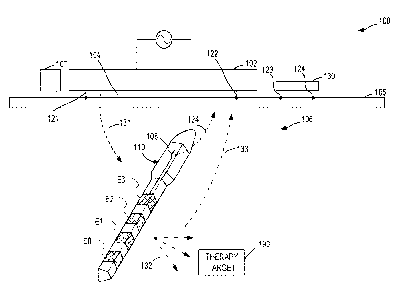
surface of the source
102 and/or to a surface of the higher-index material 106 (e.g., a surface of
the higher-index material
106 that faces the external source 102). In accordance with several
embodiments, the external
source 102 may comprise structural features and functions described in
connection with the
midfield couplers and external sources included in WIPO Publication No.
WO/2015/179225
published on November 26, 2015 and titled "MIDFIELD COUPLER".
[0128] The external source 102 can include at least a pair of outwardly
facing electrodes
121 and 122. The electrodes 121 and 122 can be configured to contact a tissue
surface, for example,
at the interface 105. In one or more examples, the external source 102 is
configured for use with a
sleeve, pocket, or other garment or accessory that maintains the external
source 102 adjacent to
the higher-index material 106, and that optionally maintains the electrodes
121 and 122 in physical
contact with a tissue surface. In one or more examples, the sleeve, pocket, or
other garment or
accessory can include or use a conductive fiber or fabric, and the electrodes
121 and 122 can be in
physical contact with the tissue surface via the conductive fiber or fabric.
[0129] In one or more examples, more than two outwardly facing electrodes
can be used
and processor circuitry on-board or auxiliary to the source 102 can be
configured to select an
19
Date Recue/Date Received 2021-01-29
CA 03052093 201.9-07-29
WO 2018/140983 PCT/US2018/016051
optimal pair or group of electrodes to use to sense farfield signal
information (e.,g., signal
information corresponding to a delivered therapy signal or to a nearfield
signal). In such
embodiments, the electrodes can operate as antennas. In one or more examples,
the source 102
includes three outwardly facing electrodes arranged as a triangle, or four
outwardly facing
electrodes arranged as a rectangle, and any two or more of the electrodes can
be selected for
sensing and/or can be electrically grouped or coupled together for sensing or
diagnostics. In one
or more examples, the processor circuitry can be configured to test multiple
different electrode
combination selections to identify an optimal configuration for sensing a
farfield signal (an
example of the processor circuitry is presented in FIG. 2A, among others).
[0130] FIG. I illustrates an embodiment of an implantable device 110, such
as can
include a multi-polar therapy delivery device configured to be implanted in
the higher-index
material 106 or in a blood vessel. In one or more examples, the implantable
device 110 includes
all or a portion of the circuitry 500 from FIG. 5, discussed in further detail
below. In one or more
examples, the implantable device 110 is implanted in tissue below the tissue-
air interface 105, In
FIG. 1, the implantable device 110 includes an elongate body and multiple
electrodes EO, El, E2,
and E3 that are axially spaced apart along a portion of the elongate body. The
implantable device
110 includes receiver and/or transmitter circuitry (not shown in FIG. I, see
e.g., FIGS. 2A, 2B,
and 4, among others) that can enable communication between the implantable
device 110 and the
external source 102.
[0131] The various electrodes EO-E3 can be configured to deliver
electrostimulation
therapy to patient tissue, such as at or near a neural or muscle target. In
one or more examples, at
least one electrode can be selected for use as an anode and at least one other
electrode can be
selected for use as a cathode to define an electrostimulation vector. In one
or more examples,
electrode El is selected for use as an anode and electrode E2 is selected for
use as a cathode.
Together, the E1-E2 combination defines an electrostimulation vector V12.
Various vectors can
be configured independently to provide a neural electrostimulation therapy to
the same or
different tissue target, such as concurrently or at different times.
[0132) In one or more examples, the source 102 includes an antenna (see.
e.g., FIG. 3)
and the implantable device 110 includes an antenna 108 (e.g., and electric
field-based or
magnetic field-based antenna). The antennas can be configured (e.g., in
length, width, shape,
material, etc.) to transmit and receive signals at substantially the same
frequency. The
Ci 03052093 2019-07-29
WO 2018/140983 PCT/US2018/016051
implantable device 110 can be configured to transmit power and/or data signals
through the
antenna 108 to the external source 102 and can receive power and/or data
signals transmitted by
the external source 102. The external source 102 and implantable device 110
can be used for
transmission and/or reception of RF signals. A transmit/receive (T/R) switch
can be used to
switch each RF port of the external source 102 from a transmit (transmit data
or power) mode to
a receive (receive data) mode. A T/R switch can similarly be used to switch
the implantable
device 110 between transmit and receive modes. See FIG. 4, among others, for
examples of T/R
switches.
101331 In one or more examples, a receive terminal on the external source
102 can be
connected to one or more components that detect a phase and/or amplitude of a
received signal
from the implantable device 110. The phase and amplitude information can be
used to program a
phase of the transmit signal, such as to be substantially the same relative
phase as a signal
received from the implantable device 110. To help achieve this, the external
source 102 can
include or use a phase-matching and/or amplitude-matching network, such as
shown in the
embodiment of FIG. 4. The phase-matching and/or amplitude matching network can
be
configured for use with a midfield antenna that includes multiple ports, such
as shown in the
embodiment of FIG. 3.
10134] Referring again to FIG. 1, in one or more examples, the implantable
device 110
can be configured to receive a midfield signal 131 from the external source
102. The midfield
signal 131 can include power and/or data signal components. In some
embodiments, a power
signal component can include one or more data components embedded therein. In
one or more
examples, the midfield signal 131 includes configuration data for use by the
implantable device
110. The configuration data can define, among other things, therapy signal
parameters, such as a
therapy signal frequency, pulse width, amplitude, or other signal waveform
parameters. In one or
more examples, the implantable device 110 can be configured to deliver an
electrostimulation
therapy to a therapy target 190, such as can include a neural target (e.g., a
nerve, or other tissue
such as a vein, connective tissue, or other tissue that includes one or more
neurons within or near
the tissue), a muscle target, or other tissue target. An electrostimulation
therapy delivered to the
therapy target 190 can be provided using a portion of a power signal received
from the external
source 102. Examples of the therapy target 190 can include nerve tissue or
neural targets, for
example including nerve tissue or neural targets at or near cervical,
thoracic, lumbar, or sacral
21
Ci 03052093 2019-07-29
WO 2018/140983 PCT/US2018/016051
regions of the spine, brain tissue, muscle tissue, abnormal tissue (e.g.,
tumor or cancerous tissue),
targets corresponding to sympathetic or parasympathetic nerve systems, targets
at or near
peripheral nerve bundles or fibers, at or near other targets selected to treat
incontinence, urinary
urge, overactive bladder, fecal incontinence, constipation, pain, neuralgia,
pelvic pain, movement
disorders or other diseases or disorders, deep brain stimulation (DBS) therapy
targets or any
other condition, disease or disorder (such as those other conditions,
diseases, or disorders
identified herein).
[0135] Delivering the electrostimulation therapy can include using a
portion of a power
signal received via the midfield signal 131, and providing a current signal to
an electrode or an
electrode pair (e.g., two or more of EO-E3), coupled to the implantable device
110, to stimulate
the therapy target 190. As a result of the current signal provided to the
electrode(s), a nearfield
signal 132 can be generated. An electric potential difference resulting from
the nearfield signal
132 can be detected remotely from the therapy delivery location. Various
factors can influence
where and whether the potential difference can be detected, including, among
other things,
characteristics of the therapy signal, a type or arrangement of the therapy
delivery electrodes, and
characteristics of any surrounding biologic tissue. Such a remotely detected
electric potential
difference can be considered a farfield signal 133. The farfield signal 133
can represent an
attenuated portion of the nearfield signal 132. That is, the nearfield signal
132 and the farfield
signal 133 can originate from the same signal or field, such as with the
nearfield signal 132
considered to be associated with a region at or near the implantable device
110 and the therapy
target 190, and with the farfield signal 133 considered to be associated with
other regions more
distal from the implantable device 110 and the therapy target 190. In one or
more examples,
information about the implantable device 110, or about a previously-provided
or future planned
therapy provided by the implantable device 110, can be encoded in a therapy
signal and detected
and decoded by the external source 102 by way of the farfield signal 133.
[0136] In one or more examples, the device 110 can be configured to provide
a series of
electrostimulation pulses to a tissue target (e.g., neural target). For
example, the device 110 can
provide multiple electrostimulation pulses separated in time, such as using
the same or different
electrostimulation vectors, to provide a therapy. In one or more examples, a
therapy comprising
multiple signals can be provided to multiple different vectors in parallel, or
can be provided in
sequence such as to provide a series or sequence of electrostimulation pulses
to the same neural
22
Ci 01052093 2019-07-29
WO 2018/140983 PCT/US2018/016051
target. Thus, even if one vector is more optimal than the others for eliciting
a patient response,
the therapy as a whole can be more effective than stimulating only the known-
optimal vector
because (1) the target may experience a rest period during periods of non-
stimulation, and/or (2)
stimulating the areas nearby and/or adjacent to the optimal target can elicit
some patient benefit.
101371 The system 100 can include a sensor 107 at or near the interface 105
between air
104 and the higher-index material 106. The sensor 107 can include, among other
things, one or
more electrodes, an optical sensor, an accelerometer, a temperature sensor, a
force sensor, a
pressure sensor, or a surface electromyography (EMG) device. The sensor 107
may comprise
multiple sensors (e.g., two, three, four or more than four sensors). Depending
on the type of
sensor(s) used, the sensor 107 can be configured to monitor electrical,
muscle, or other activity
near the device 110 and/or near the source 102. For example, the sensor 107
can be configured to
monitor muscle activity at a tissue surface. If muscle activity greater than a
specified threshold
activity level is detected, then a power level of the source 102 and/or of the
device 110 can be
adjusted. In one or more examples, the sensor 107 can be coupled to or
integrated with the
source 102, and in other examples, the sensor 107 can be separate from, and in
data
communication with (e.g., using a wired or wireless electrical coupling or
connection), the
source 102 and/or the device 110.
101381 The system 100 can include a farfield sensor device 130 that can be
separate
from, or communicatively coupled with, one or more of the source 102 and the
sensor 107. The
farfield sensor device 130 can include two or more electrodes and can be
configured to sense a
farfield signal, such as the farfield signal 133 corresponding to a therapy
delivered by the device
110. The farfield sensor device 130 can include at least one pair of outwardly
facing electrodes
123 and 124 configured to contact a tissue surface, for example, at the
interface 105. In one or
more examples, three or more electrodes can be used, and processor circuitry
on-board or
auxiliary to the farfield sensor device 130 can select various combinations of
two or more of the
electrodes for use in sensing the farfield signal 133. In one or more
examples, the farfield sensor
device 130 can be configured for use with a sleeve, pocket, or other garment
or accessory that
maintains the farfield sensor device 130 adjacent to the higher-index material
106, and that
optionally maintains the electrodes 123 and 124 in physical contact with a
tissue surface. In one
or more examples, the sleeve, pocket, or other garment or accessory can
include or use a
conductive fiber or fabric, and the electrodes 123 and 124 can be in physical
contact with the
23
Ci 03052093 2019-07-29
WO 2018/140983 PCT/US2018/016051
tissue surface via the conductive fiber or fabric. An example of at least a
portion of a farfield
sensor device 130 is further described herein in connection with FIG. 213.
[0139] In one or more examples, the external source 102 provides a midfield
signal 131
including power and/or data signals to the implantable device 110. The
midfield signal 131
includes a signal (e.g., an RI, signal) having various or adjustable
amplitude, frequency, phase,
and/or other signal characteristics. The implantable device 110 can include an
antenna, such as
described below, that can receive the midfield signal 131 and, based on
characteristics of
receiver circuitry in the implantable device 110, can modulate the received
signal at the antenna
to thereby generate a backscatter signal. In one or more examples, the
implantable device 110
can encode information in the backscatter signal 112, such as information
about a characteristic
of the implantable device 110 itself, about a received portion of the midfield
signal 131, about a
therapy provided by the implantable device 110, and/or other information. The
backscatter signal
112 can be received by an antenna at the external source 102 and/or the
farfield sensor device
130, or can be received by another device. In one or more examples, a
biological signal can be
sensed by a sensor of the implantable device 110, such as a glucose sensor, an
electropotential
(e.g., an electromyography sensor, electrocardiograph (ECG) sensor,
resistance, or other
electrical sensor), a light sensor, a temperature, a pressure sensor, an
oxygen sensor, a motion
sensor, or the like. A signal representative of the detected biological signal
can be modulated
onto the backscatter signal 112. Other sensors are discussed elsewhere herein,
such as with
regard to FIG. 81, among others. In such embodiments, the sensor 107 can
include a
corresponding monitor device, such as a glucose, temperature, ECG, EMG,
oxygen, or other
monitor, such as to receive, demodulate, interpret, and/or store data
modulated onto the
backscatter signal.
[0140] In one or more examples, the external source 102 and/or the
implantable device
110 can include an optical transceiver configured to facilitate communication
between the
external source 102 and the implantable device 110. The external source 102
can include a light
source, such as a photo laser diode or LED, or can include a photo detector,
or can include both
of a light source and a photo detector. The implantable device 110 can include
a light source,
such as a photo laser diode or LED, or can include a photo detector, or can
include both of a light
source and a photo detector. In an example, the external source 102 and/or
implantable device
24
Ci 03052093 2019-07-29
WO 2018/140983 PCT/US2018/016051
110 can include a window, such as made of quartz, Wass, or other translucent
material, adjacent
to its light source or photo detector.
[0141] In an example, optical communications can be separate from or
supplemental to
an electromagnetic coupling between the external source 102 and the
implantable device 110.
Optical communication can be provided using light pulses modulated according
to various
protocols, such as using pulse position modulation (PPM). In an example, a
light source and/or
photo detector on-board the implantable device 110 can be powered by a power
signal received
at least in part via midfield coupling with the external source 102.
101421 In an example, a light source at the external source 102 can send a
communication
signal through skin, into subcutaneous tissue, and through an optical window
(e.g., quartz
window) in the implantable device 110. The communication signal can be
received at a photo
detector on-board the implantable device 110. Various measurement information,
therapy
information, or other information from or about the implantable device can be
encoded and
transmitted from the implantable device 110 using a light source provided at
the implantable
device 110. The light signal emitted from the implantable device 110 can
travel through the same
optical window, subcutaneous tissue, and skin tissue, and can be received at
photo detector on-
board the external source 102. In an example, the light sources and/or photo
detectors can be
configured to emit and/or receive, respectively, electromagnetic waves in the
visible or infrared
ranges, such as in a range of about 670 ¨910 nm wavelength (e.g., 670 run ¨
800 nm, 700 nm
760 nm, 670 nm ¨ 870 nm, 740 mn ¨ 850 nm, 800 nm ¨ 910 nm, overlapping ranges
thereof, or
any value within the recited ranges).
[0143] FIG. 2A illustrates, by way of example, a block diagram of and
embodiment of a
midfield source device, such as the external source 102 The external source
102 can include
various components, circuitry, or functional elements that are in data
communication with one
another. In the example of FIG. 2A, the external source 102 includes
components, such as
processor circuitry 210, one or more sensing electrodes 220 (e.g., including
the electrodes 121
and 122), a demodulator circuitry 230, a phase-matching or amplitude-matching
network 400, a
midfield antenna 300, and/or one or more feedback devices, such as can include
or use an audio
speaker 251, a display interface 252, and/or a haptic feedback device 253. The
midfield antenna
300 is further described below in the embodiment of FIG. 3, and the network
400 is further
described below in the embodiment of FIG. 4. The processor circuitry 210 can
be configured to
Ci 03052093 2019-07-29
WO 2018/140983 PCT/US2018/016051
coordinate the various functions and activities of the components, circuity,
and/or functional
elements of the external source 102.
[0144] The midfield antenna 300 can be configured to provide a midfield
excitation
signal, such as can include RF signals having a non-negligible H-field
component that is
substantially parallel to an external tissue surface. In one or more examples,
the RF signals can
be adapted or selected to manipulate an evanescent field at or near a tissue
surface, such as to
transmit a power and/or data signal to respective different target devices
(e.g., the implantable
device 110, or any one or more other implantable devices discussed herein)
implanted in tissue.
The midfield antenna 300 can be further configured to receive backscafter or
other wireless
signal information that can be demodulated by the demodulator circuitry 230.
The demodulated
signals can be interpreted by the processor circuitry 210. The midfield
antenna 300 can include
a dipole antenna, a loop antenna, a coil antenna, a slot or strip antenna, or
other antenna. The
antenna 300 can be shaped and sized to receive signals in a range of between
about 400 MHz and
about 4 GHz (e.g., between 400 MHz and 1 GHz, between 400 MHz and 3 GHz,
between 500
MHz and 2 GHz, between I GHz and 3 GHz, between 500 MHz and 1.5 GHz, between 1
GHz
and 2 GHz, between 2 GHz and 3 Gliz, overlapping ranges thereof, or any value
within the
recited ranges). For embodiments incorporating a dipole antenna, the midfield
antenna 300 may
comprise a straight dipole with two substantially straight conductors, a
folded dipole, a short
dipole, a cage dipole, a bow-tie dipole or batwing dipole.
[0145] The demodulator circuitry 230 can be coupled to the sensing
electrodes 220. In
one or more examples, the sensing electrodes 220 can be configured to receive
the farfield signal
133, such as based on a therapy provided by the implantable device 110, such
as can be delivered
to the therapy target 190 The therapy can include an embedded or intermittent
data signal
component that can be extracted from the farfield signal 133 by the
demodulator circuitry 230.
For example, the data signal component can include an amplitude-modulated or
phase-modulated
signal component that can be discerned from background noise or other signals
and processed by
the demodulator circuitry 230 to yield an information signal that can be
interpreted by the
processor circuitry 210. Based on the content of the information signal, the
processor circuitry
210 can instruct one of the feedback devices to alert a patient, caregiver, or
other system or
individual. For example, in response to the information signal indicating
successful delivery of a
specified therapy, the processor circuitry 210 can instruct the audio speaker
251 to provide
26
Ci 03052093 2019-07-29
WO 2018/140983 PCT/US2018/016051
audible feedback to a patient, can instruct the display interface 252 to
provide visual or graphical
information to a patient, and/or can instruct the haptic feedback device 253
to provide a haptic
stimulus to a patient. In one or more examples, the haptic feedback device 253
includes a
transducer configured to vibrate or to provide another mechanical signal.
101461 FIG. 2B illustrates generally a block diagram of a portion of a
system configured
to receive a farfield signal. The system can include the sensing electrodes
220, such as can
include the electrodes 121 and 122 of the source 102, or the electrodes 123
and 124 of the
farfield sensor device 130. In the example of FIG. 2B, there are at least four
sensing electrodes
represented collectively as the sensing electrodes 220, and individually as
SEO, SE1, SE2, and
SE3; however, other numbers of sensing electrodes 220 may also be used. The
sensing electrodes
can be communicatively coupled to multiplexer circuitry 261. The multiplexer
circuitry 261 can
select pairs of the electrodes, or electrode groups, for use in sensing
farfield signal information.
In one or more examples, the multiplexer circuitry 261 selects an electrode
pair or grouping
based on a detected highest signal to noise ratio of a received signal, or
based on another relative
indicator of signal quality, such as amplitude, frequency content, and/or
other signal
characteristic.
[0147] Sensed electrical signals from the multiplexer circuitry 261 can
undergo various
processing to extract information from the signals. For example, analog
signals from the
multiplexer circuitry 261 can be filtered by a band pass filter 262. The band
pass filter 262 can
be centered on a known or expected modulation frequency of a sensed signal of
interest. A band
pass filtered signal can then be amplified by a low-noise amplifier 263. The
amplified signal can
be converted to a digital signal by an analog-to-digital converter circuitry
(ADC) 264. The digital
signal can be further processed by various digital signal processors 265, as
further described
herein, such as to retrieve or extract an information signal communicated by
the implantable
device 110.
[0148] FIG. 3 illustrates generally a schematic view of an embodiment of a
midfield
antenna 300 with multiple subwavelength structures 301, 302, 303, and 304. The
midfield
antenna 300 can include a midfield plate structure with a planar surface. The
one or more
subwavelength structures 301-304 can be formed in the plate structure. In the
example of FIG. 3,
the antenna 300 includes a first subwavelength structure 301, a second
subwavelength structure
302, a third subwavelength structure 303, and a fourth subwavelength structure
304. Fewer or
27
CA 03052093 2019-07-29
WO 2018/140983 PCT/US2018/016051
additional subwavelength structures can be used. The subwavelength structures
can be excited
individually or selectively by one or more RF ports (e.g., first through
fourth RF ports 311, 312,
313, and 314) respectively coupled thereto. A "subwavelength structure" can
include a hardware
structure with dimensions defined relative to a wavelength of a field that is
rendered and/or
received by the external source 102. For example, for a given X.0
corresponding to a signal
wavelength in air, a source structure that includes one or more dimensions
less than A.0 can be
considered to be a subwavelength structure. Various designs or configurations
of subwavelength
structures can be used. Some examples of a subwavelength structure can include
a slot in a
planar structure, or a strip or patch of a conductive sheet of substantially
planar material.
[0149] FIG. 4 illustrates generally the phase-matching or amplitude-
matching network
400. In an example, the network 400 can include the antenna 300, and the
antenna 300 can be
electrically coupled to a plurality of switches 404A, 404B, 404C, and 404D,
for example, via the
first through fourth RF ports 311, 312, 313, and 314 illustrated in FIG. 3.
The switches 404A-D
are each electrically coupled to a respective phase and/or amplitude detector
406A, 406B, 406C,
and 406D, and a respective variable gain amplifier 408A, 408B, 408C, and 408D.
Each amplifier
408A-D is electrically coupled to a respective phase shifter 410A, 410B, 410C,
and 410D, and
each phase shifter 410A-D is electrically coupled to a common power divider
412 that receives
an RF input signal 414 to be transmitted using the external source 102.
[0150] In one or more examples, the switches 404A-D can be configured to
select either
a receive line ("R") or a transmit line (-le). A number of switches 404A-D of
the network 400
can be equal to a number of ports of the midfield source 402. In the example
of the network 400,
the midfield source 402 includes four ports (e.g., corresponding to the four
subwavelength
structures in the antenna 300 of the example of FIG. 3), however any number of
ports (and
switches), such as one, two, three, four, five, six, seven, eight or more, can
be used.
[0151] The phase and/or amplitude detectors 406A-1) are configured to
detect a phase
(4)1, (1)2, (1)3, 44) and/or power (P1, P2, P3, P4) of a signal received at
each respective port of
the midfield source 402. In one or more examples, the phase and/or amplitude
detectors 406A-D
can be implemented in one or more modules (hardware modules that can include
electric or
electronic components arranged to perform an operation, such as determining a
phase or
amplitude of a signal), such as including a phase detector module and/or an
amplitude detector
28
Ci 03052093 2019-07-29
WO 2018/140983 PCT/US2018/016051
module. The detectors 406A-D can include analog and/or digital components
arranged to
produce one or more signals representative of a phase and/or amplitude of a
signal received at
the external source 102.
10152] The amplifiers 408A-D can receive respective inputs from the phase
shifters
410A-D (e.g., Pk phase shifted by 0k, 01 + 0k, 02 + 0k, 03 + 0k, or 04 + 0k).
The output of
the amplifier, 0, is generally the output of the power divider, M when the RF
signal 414 has an
amplitude of 4*M (in the embodiment of FIG. 4), multiplied by the gain of the
amplifier Pi*Pk.
Pk can be set dynamically as the values for Pl, P2, P3, and/or P4 change. Ok
can be a constant.
In one or more examples, the phase shifters 410A-D can dynamically or
responsively configure
the relative phases of the ports based on phase information received from the
detectors 406A-D.
101531 In one or more examples, a transmit power requirement from the
midfield source
402 is Pit. The RF signal provided to the power divider 412 has a power of
4*M. The output of
the amplifier 408A is about M* P1 *Pk. Thus, the power transmitted from the
midfield coupler is
M*(Pl*Pk + P2*Pk + P3*Pk + P4*Pk)= Ptt. Solving for Pk yields Pk = Ptt /
(M*(P1 + P2 P3
+ P4)).
10154] The amplitude of a signal at each RF port can be transmitted with
the same
relative (scaled) amplitude as the signal received at the respective port of
the midfield coupler
coupled thereto. The gain of the amplifiers 408A-1) can be further refined to
account for any
losses between the transmission and reception of the signal from the midfield
coupler. Consider a
reception efficiency of ii = Pir/Ptt, where Pir is the power received at the
implanted receiver. An
efficiency (e.g., a maximum efficiency), given a specified phase and amplitude
tuning, can be
estimated from an amplitude received at the external midfield source from the
implantable
source. This estimation can be given asilz-- (Pl+P2+P3+P4)/Pit, where Pit is
an original power
of a signal from the implanted source. Information about a magnitude of the
power transmitted
from the implantable device 110 can be communicated as a data signal to the
external source
102. In one or more examples, an amplitude of a signal received at an
amplifier 408A-D can be
scaled according to the determined efficiency, such as to ensure that the
implantable device
receives power to perform one or more programmed operation(s). Given the
estimated link
efficiency, n, and an implant power (e.g., amplitude) requirement of Pir', Pk
can be scaled as
Pk=Pir'/[1(P1+P2+P3+P4)], such as to help ensure that the implant receives
adequate power to
perform the programmed functions.
29
Ci 03052093 2019-07-29
WO 2018/140983 PCT/US2018/016051
[0155] Control signals for the phase shifters 410A-D and the amplifiers
408A-D, such as
the phase input and gain input, respectively, can be provided by processing
circuitry that is not
shown in FIG. 4. The circuitry is omitted to not overly complicate or obscure
the view provided
in FIG. 4. The same or different processing circuitry can be used to update a
status of one or
more of the switches 404A-D between receive and transmit configurations. See
the processor
circuitry 210 of FIG. 2A and its associated description for an example of
processing circuitry.
[0156] FIG. 5 illustrates generally a diagram of an embodiment of circuitry
500 of the
implantable device 110, or target device, such as can include an elongate
device and such as can
optionally be deployed inside a blood vessel, according to one or more of the
embodiments
discussed herein. The circuitry 500 includes one or more pad(s) 536, such as
can be electrically
connected to the antenna 108. The circuitry 500 can include a tunable matching
network 538 to
set an impedance of the antenna 108 based on an input impedance of the
circuitry 500. The
impedance of the antenna 108 can change, for example, due to environmental
changes. The
tunable matching network 538 can adjust the input impedance of the circuitry
500 based on the
varying impedance of the antenna 108. In one or more examples, the impedance
of the tunable
matching network 538 can be matched to the impedance of the antenna 108. In
one or more
examples, the impedance of the tunable matching network 538 can be set to
cause a portion of a
signal incident on the antenna 108 reflect back from the antenna 108, thus
creating a backscatter
signal.
[0157] A transmit-receive (T/R) switch 541 can be used to switch the
circuitry 500 from
a receive mode (e.g., in which power and/or data signals can be received) to a
transmit mode
(e.g., in which signals can be transmitted to another device, implanted or
external). An active
transmitter can operate at an Industrial, Scientific. and Medical (ISM) band
of 2.45 GHZ or 915
MHz, or the 402 MHz Medical Implant Communication Service (MICS) band for
transferring
data from the implant. Alternatively, data can be transmitted using a Surface
Acoustic Wave
(SAW) device that backscatters incident radio frequency (RF) energy to the
external device.
[0158] The circuitry 500 can include a power meter 542 for detecting an
amount of
received power at the implanted device. A signal that indicates power from the
power meter 542
can be used by a digital controller 548 to determine whether received power is
adequate (e.g.,
above a specified threshold) for the circuitry to perform some specified
function. A relative value
of a signal produced by the power meter 542 can be used to indicate to a user
or machine
Ci 03052093 2019-07-29
WO 2018/140983 PCT/US2018/016051
whether an external device (e.g., the source 102) used to power the circuitry
500 is in a suitable
location for transferring power and/or data to the target device.
[0159] In one or more examples, the circuitry 500 can include a demodulator
544 for
demodulating received data signals. Demodulation can include extracting an
original
information-bearing signal from a modulated carrier signal. In one or more
examples, the
circuitry 500 can include a rectifier 546 for rectifying a received AC power
signal.
[0160] Circuity (e.g., state logic, Boolean logic, or the like) can be
integrated into the
digital controller 548. The digital controller 548 can be configured to
control various functions of
the receiver device, such as based on the input(s) from one or more of the
power meter 542,
demodulator 544, and/or the clock 550. In one or more examples, the digital
controller 548 can
control which electrode(s) (e.g., EO-E3) are configured as a current sink
(anode) and which
electrode(s) are configured as a current source (cathode). In one or more
examples, the digital
controller 548 can control a magnitude of a stimulation pulse produced through
the electrode(s).
[0161] A charge pump 552 can be used to increase the rectified voltage to a
higher
voltage level, such as can be suitable for stimulation of the nervous system.
The charge pump
552 can use one or more discrete components to store charge for increasing the
rectified voltage.
In one or more examples, the discrete components include one or more
capacitors, such as can be
coupled to pad(s) 554. In one or more examples, these capacitors can be used
for charge
balancing during stimulation, such as to help avoid tissue damage.
[0162] A stimulation driver circuitry 556 can provide programmable
stimulation through
various outputs 534, such as to an electrode array. The stimulation driver
circuitry 556 can
include an impedance measurement circuitry, such as can be used to test for
correct positioning
of the electrode(s) of the array. The stimulation driver circuitry 556 can be
programmed by the
digital controller to make an electrode a current source, a current sink, or a
shorted signal path.
The stimulation driver circuitry 556 can be a voltage or a current driver. The
stimulation driver
circuitry 556 can include or use a therapy delivery circuitry that is
configured to provide
electrostimulation signal pulses to one or more electrodes, such as using at
least a portion of a
received midfield power signal from the external source 102. In one or more
examples, the
stimulation driver circuitry 556 can provide pulses at frequencies up to about
100 kHz. Pulses at
frequencies around 100 kHz can be useful for nerve blocking.
31
Ci 03052093 2019-07-29
WO 2018/140983 PCT/US2018/016051
[0163] The circuitry 500 can further include a memory circuitry 558, such
as can include
a non-volatile memory circuitry. The memory circuitry 558 can include storage
of a device
identification, neural recordings, and/or programming parameters, among other
implant related
data.
[0164] The circuitry 500 can include an amplifier 555 and analog digital
converter
(ADC) 557 to receive signals from the electrode(s). The electrode(s) can sense
electricity from
nerve signals within the body. The nerve signals can be amplified by the
amplifier 555 These
amplified signals can be converted to digital signals by the ADC 557. These
digital signals can
be communicated to an external device. The amplifier 555, in one or more
examples, can be a
trans-impedance amplifier.
[0165] The digital controller 548 can provide data to a modulator/power
amplifier 562.
The modulator/power amplifier 562 modulates the data onto a carrier wave. The
power amplifier
562 increases the magnitude of the modulated wavefonn to be transmitted.
[0166] The modulator/power amplifier 562 can be driven by an
oscillator/phase locked
loop (PLL) 560. The PLL disciplines the oscillator so that it remains more
precise. The oscillator
can optionally use a different clock from the clock 550. The oscillator can be
configured to
generate an RF signal used to transmit data to an external device. A typical
frequency range for
the oscillator is about 10 kHz to about 2600 MHz (e.g., from 10 kHz to 1000
MHz, from 500
kHz to 1500 kHz, from 10 kHz to 100 kHz, from 50 kHz to 200 kHz, from 100 IcHz
to 500 kHz,
from 100 lcHz to 1000 kHz, from 500 kHz to 2 MHz, from 1 MHz to 2 MHz, from 1
MHz to 10
MHz, from 100 MHz to 1000 MHz, from 500 MHz to 2500 MHz, overlapping ranges
thereof, or
any value within the recited ranges). Other frequencies can be used, such as
can be dependent on
the application. The clock 550 is used for timing of the digital controller
548. A typical
frequency of the clock 550 is between about one kilohertz and about one
megahertz (e.g.,
between 1 kHz and 100 kHz, between 10 kHz and 150 kHz, between 100 kHz and 500
kHz,
between 400 kHz and 800 kHz, between 500 kHz and 1 MHz, between 750 kHz and 1
MHz,
overlapping ranges thereof, or any value within the recited ranges). Other
frequencies can be
used depending on the application. A faster clock generally uses more power
than a slower
clock
32
CA 03052093 201.9-07-29
WO 2018/140983 PCT/US2018/016051
[0167] A return path for a signal sensed from a nerve is optional. Such a
path can include
the amplifier 555, the ADC 557, the oscillator/PLL 560, and the
modulator/power amplifier 562.
Each of these items and connections thereto can optionally be removed.
10168] In one or more examples, the digital controller 548, the amplifier
555, and/or the
stimulation driver circuitry 556, among other components of the circuitry 500,
can comprise
portions of a state machine device. The state machine device can be configured
to wirelessly
receive power and data signals via the pad(s) 536 and, in response, release or
provide an
electrostimulation signal via one or more of the outputs 534. In one or more
examples, such a
state machine device needs not retain information about available
electrostimulation settings or
vectors, and instead the state machine device can carry out or provide
electrostimulation events
after, and/or in response to, receipt of instructions from the source 102.
[0169] For example, the state machine device can be configured to receive
an instruction
to deliver a neural electrostimulation therapy signal, such as at a specified
time or having some
specified signal characteristic (e.g., amplitude, duration, etc.), and the
state machine device can
respond by initiating or delivering the therapy signal at the specified time
and/or with the
specified signal characteristic(s). At a subsequent time, the device can
receive a subsequent
instruction to terminate the therapy, to change a signal characteristic, or to
perform some other
task Thus, the device can optionally be configured to be substantially
passive, or can be
configured to be responsive to received instructions (e.g., contemporaneously
received
instructions).
A. CIRCUITRY HOUSING ASSEMBLIES
[0170] This section describes embodiments and/or features of therapy
devices, guiding
mechanisms for situating an implantable device (e.g, the therapy device)
within tissue, and/or
affixing mechanisms for helping ensure the implantable device does not
appreciably move when
situated within the tissue. One or more examples regard therapy devices for
treatment of
incontinence (e.g., urinary incontinence, fecal incontinence), overactive
bladder. pain or other
conditions or symptoms, such as those described elsewhere herein.
[0171] An advantage of an implantable device discussed in this section (and
others) can
include one or more of: (i) a configurable implantable device that can be
altered in shape and/or
33
CA 03052093 2019-07-29
WO 2018/140983 PCT/US2018/016051
electrode configuration to help target a site for electrostimulation within a
body; (ii) an
implantable device that can be implanted and then affixed at a target location
(such as an S3
foramen); (iii) an implantable device with improved signal reception
efficiency (e.g., using (1) a
dielectric material surrounding an antenna, the dielectric material including
a dielectric constant
that is between a dielectric constant of human tissue and that of air, or (2)
multiple antennas in
the implantable device, such as to include a primary antenna inductively
coupled to a secondary
antenna), (iv) a thin, discreet implantable device that can be implanted in
narrow areas or thin
tissue, such as between skin and bone; (v) an implantable device that can
provide an
electrostimulation pattern that an elongated tubular implantable device is not
able to provide
(e.g., due to the location of the electrodes and shape of the implantable
device); and/or (vi) a
network of implantable devices that can provide a local or wide area
stimulation individually or
in combination, among others.
[0172] In accordance with several embodiments, a system includes an
implantable device
comprising an elongated member having a distal portion and a proximal portion.
The device
includes a plurality of electrodes, a circuitry housing, circuitry within the
circuitry housing
adapted to provide electrical energy to the plurality of electrodes, an
antenna housing, and an
antenna (e.g., a helical antenna) in the antenna housing. The plurality of
electrodes is situated or
located along the distal portion of the elongated member. 'The circuitry
housing is attached to the
proximal portion of the elongated member. The circuitry is hermetically sealed
or encased within
the circuitry housing. The antenna housing is attached to the circuitry
housing at a proximal end
of the circuitry housing opposite to an end of the circuitry housing attached
to the elongated
member.
(0173) The system may optionally comprise an external midfield power source
adapted
to provide a power or electrical signal or energy to the implantable device.
The implantable
device may be adapted to communicate information (e.g., data signals) to an
antenna of the
external source via the antenna. One, more than one or all the electrodes may
optionally be
located at a proximal portion or central portion of the elongated member
instead of the distal
portion. The circuitry housing may optionally be attached to a distal portion
or central portion of
the elongated member. The antenna housing may not be attached to the circuitry
housing or may
not be attached to the proximal end of the circuitry housing. The antenna
housing may optionally
include a dielectric material with a dielectric constant between that of human
tissue and air, such
34
Ci 03052093 2019-07-29
WO 2018/140983 PCT/US2018/016051
as a ceramic material. The ceramic material may optionally cover the antenna.
The elongated
member may optionally be flexible and/or cylindrical. The electrodes may
optionally be
cylindrically-shaped and positioned around a circumference of the elongated
member.
[0174] The elongated member may optionally include a channel extending
through the
elongated member from a proximal end of the member to the distal portion of
the elongated
member and a memory metal wire situated in the channel, the memory metal wire
pre-shaped in
an orientation to provide curvature to the elongated member. The memory metal
may optionally
be shaped to conform to a shape of an S3 foramen and generally match a curve
of a sacral nerve
The antenna may be a primary antenna and the device may further include a
secondary antenna
in a housing attached to the antenna housing, the secondary antenna shaped and
positioned to
provide a near field coupling with the primary antenna. The device may
optionally include one or
more sutures attached at one or more of: (1) a proximal portion of the antenna
housing; (2) a
proximal portion of the circuitry housing; and (3) an attachment structure
attached to a proximal
end of the antenna housing. The antenna may optionally be coupled to a
conductive loop of the
circuitry situated in a proximal portion of the circuitry housing. There may
be a ceramic material
between the antenna and the conductive loop.
[0175] There is an ongoing desire to reduce a displacement volume of
implantable sensor
and/or stimulator devices, such as including neurostimulation devices.
Additional miniaturization
can allow for an easier less invasive implant procedure, reduce a surface area
of the implantable
device which can in turn reduce a probability of post-implant infection, and
provide patient
comfort in a chronic ambulatory patient setting. In some examples, a
miniaturized device can be
injected using a catheter or carmula, further reducing invasiveness of an
implant procedure.
[0176] In an example, a configuration of an implantable neurostimulation
device is
different from a conventional lead implanted with a pulse generator. The
implantable stimulation
device can include a lead-less design and can be powered from a remote source
(e.g., a midfield
source located distal to the implantable device).
[0177] In an example, a method of making an implantable stimulation device
can include
forming electrical connections at both ends of a circuitry housing, such as
can be a hermetically
sealed circuitry housing. The method can include forming electrical
connections between a
feedthrough assembly and pads of a circuit board. In an example, the
feedthrough assembly
includes a cap-like structure inside of which electrical and/or electronic
components can be
Ci 01052093 2019-07-29
WO 2018/140983 PCT/US2018/016051
provided. A surface of the pads of the circuit board can be generally
perpendicular to a surface of
an end of feedthroughs of the feedthrough assembly.
[0178] The method can be useful in, for example, forming a hermetic
circuitry housing,
such as can be part of an implantable stimulation device or other device that
can be exposed to
liquid or other environmental elements that can adversely affect electrical
and/or electronic
components.
[0179] Various traditional assembly techniques can be difficult to apply to
miniature
devices such as implantable or injectable stimulator devices. For example,
wirebonding can be
difficult since connections to the substrate may be on a surface that is
generally perpendicular to
a feedthrough. In some examples, wirebonds can be compressed when the
circuitry housing is
sealed. Using thin wires that can be compressed to make connections between
the substrate and
the board, however, can increase parasitic capacitance and/or inductance of
the RF feedthrough
and may detune an RF receiving structure. Further, manufacturing yield may be
limited through
such compression and/or thin wires. The compression can break a bond between a
wire and a pad
or can break the wire itself. The thickness of the wire can affect how likely
the wire is to break,
for example because a thin wire can be more likely to break, when compressed,
than a thicker
wire.
[0180] FIG. 6 illustrates generally a diagram of an embodiment of a first
implantable
device 600. The device 600 includes a body portion 602, multiple electrodes
604, a circuitry
housing 606, and an antenna housing 608. The antenna housing 608 encapsulates
an antenna
MO. The implantable device 600 can be configured to sense electrical (or
other) activity
information from a patient, or to deliver an electrostimulation therapy to the
patient such as using
one or more of the electrodes 604.
[0181] The body portion 602 can be made of a flexible or rigid material. In
one or more
examples, the body portion 602 can include a bio-compatible material. The body
portion 602 can
include, among other materials, platinum, iridium, titanium, ceramic,
Zirconia, alumina, glass,
polyurethane, silicone, epoxy, and/or a combination thereof.
[0182] The body portion 602 includes one or more electrodes 604 thereon or
at least
partially therein. The electrodes 604, as illustrated in the example of FIG.
6, are ring electrodes.
In the example of FIG. 6, the electrodes 604 are substantially evenly
distributed along the body
portion, that is, a substantially equal space is provided between adjacent
electrodes. Other
36
Ci 03052093 2019-07-29
WO 2018/140983 PCT/US2018/016051
electrode configurations can additionally or alternatively be used. Some
examples of other
electrode configurations are illustrated herein at, e.g., FIGS. 30A-40.
[0183] The body portion 602 can include, or can be coupled to, a circuitry
housing 606.
In an example, the circuitry housing 606 is coupled to the body portion 602 at
a first end 601 of
the body portion 602. In the example of FIG. 6, the first end 601 of the body
portion 602 is
opposite a second end 603 of the body portion 602.
[0184] The circuitry housing 606 can provide a hermetic seal for electric
and/or
electronic components 712 (see, e.g., FIG. 7) and/or interconnects housed
therein. The electrodes
604 can be respectively electrically connected to circuitry in the circuitry
housing 606 using one
or more feedthroughs and one or more conductors, such as is illustrated and
described herein.
That is, the circuitry housing 606 can provide a hermetic enclosure for the
electronic components
712 (e.g., electric and/or electronic components provided inside or
encapsulated by the circuitry
housing 606).
[0185] In an example, the antenna housing 608 is attached to the circuitry
housing 606 at
a first side end 711 (see, e.g., FIG. 7) of the circuitry housing 606. An
antenna 610 can be
provided inside the antenna housing 608. In an example, the antenna 610 is
used for receiving at
and/or transmitting from the device 1200 power and/or data signals. The first
side end 711 is
opposite a second side end 713 of the circuitry housing 606. In an example,
the second side end
713 is an end to which an electrode assembly, such as including the electrodes
604, or other
assembly, can be electrically connected.
[0186] The antenna housing 608 can be coupled to the circuitry housing 606
in various
ways or using various connective means. For example, the antenna housing 608
can be brazed
(e.g., using gold or other conductive or non-conductive material) to the
circuitry housing 606.
The antenna housing 608 can include an epoxy, tecothane, or other
substantially radio frequency
(RF) transparent (e.g., at a frequency used to communicate to/from the device
1200) and
protective material.
[0187] In one or more examples, the antenna housing 608 can include a
ceramic material
such as zirconia or alumina. The dielectric constant of zirconia is similar to
a dielectric constant
of typical body muscle tissue. Using a material with a dielectric constant
similar to that of
muscle tissue can help stabilize the circuit impedance of the antenna 610 and
can decrease a
change in impedance when the antenna 610 is surrounded by different tissue
types.
37
Ci 03052093 2019-07-29
WO 2018/140983 PCT/US2018/016051
[0188] A power transfer efficiency such as from an external transmitter to
the device
1200 can be influenced by the selection of antenna or housing materials. For
example, a power
transfer efficiency of the device 1200 can be increased when the antenna 610
is surrounded or
encapsulated by a lower permittivity tissue, such as when the antenna housing
608 comprises a
ceramic material. In an example, the antenna 610 can be composed as a single
ceramic structure
with the feedtivough.
[0189] FIG. 7 illustrates generally a schematic view of an embodiment of
the circuitry
housing 606. The circuitry housing 606 as illustrated includes various
electric and/or electronic
components 712A, 712B, 712C, 712D, 712E, 712F, and 712G, such as can be
electrically
connected to a circuit board 714. The components 712A-G and the circuit board
714 are situated
within an enclosure 722. In an example, the enclosure 722 comprises a portion
of the circuitry
housing 606.
[0190] One or more of the components 712A-G can include one or more
transistors,
resistors, capacitors, inductors, diodes, central processing units (CPUs),
field programmable gate
arrays (FPGAs), Boolean logic gates, multiplexers, switches, regulators,
amplifiers, power
sources, charge pumps, oscillators, phase locked loops (PLLs), modulators,
demodulators, radios
(receive and/or transmit radios), and/or antennas (e.g., a helical shaped
antenna, a coil antenna, a
loop antenna, or a patch antenna, among others), or the like. The components
712A-G in the
circuitry housing 606 can be arranged or configured to form, among other
things, stimulation
therapy generation circuitry configured to provide stimulation therapy
signals, such as can be
delivered to a body using the electrodes 604, receiver circuitry configured to
receive power
and/or data from a remote device, transmitter circuitry configured to provide
data to a remote
device, and/or electrode selection circuitry such as configured to select
which of the electrodes
604 is configured as one or more anodes or cathodes.
[0191] The enclosure 722 can include a platinum and iridium alloy (e.g.,
90/10, 80/20,
95/15, or the like), pure platinum, titanium (e.g., commercially pure, 6A1/4V
or another alloy),
stainless steel, or a ceramic material (such as zirconia or alumina, for
example), or other
hermetic, biocompatible material. The circuitry housing 606 and/or the
enclosure 722 can
provide an airtight space for the circuitry therein. A thickness of a sidewall
of the enclosure 722
can be about tens of micrometers, such as can be about ten, twenty, thirty,
forty, fifty, sixty,
seventy, eighty, ninety, one hundred, one hundred ten, etc. micrometers, or
some thickness in
38
Ci 01052093 2019-07-29
WO 2018/140983 PCT/US2018/016051
between. An outer diameter of the enclosure 722 can be on the order of less
than ten millimeters,
such as can be about one, one and a half, two, two and a half, three, three
and a half, etc.
millimeters or some outer diameter in between. A length of the enclosure can
be on the order of
millimeters, such as can include two, three, four, five, six, seven, eight,
nine, ten, eleven, twelve,
thirteen, etc. millimeters, or some length in between. If a metallic material
is used for the
enclosure 722, the enclosure 722 can be used as part of the electrode array,
effectively increasing
the number of selectable electrodes 604 for stimulation
[0192] Rather than being hermetic, the enclosure 722 can be backfilled to
prevent ingress
of moisture therein. The backfill material can include a non-conductive,
waterproof material,
such as epoxy, parylene, tecothane, or other material or combination of
materials.
[0193] In the example of FIG. 7, the circuitry housing 606 can include a
first end cap
716A and a second end cap 716B. In an example, the caps 716A and 716B are
situated on or at
least partially in the enclosure 722. The caps 716A and 716B can be provided
to cover openings
such as on substantially opposite sides of the enclosure 722. The cap 716A
forms a portion of the
first side end 711 of the circuitry housing 606 and the cap 716B forms a
portion of the second
side end 713 of the circuitry housing 606. Each of the caps 716A-B includes
one or more
conductive feedthroughs. In the example of FIG. 7, the first end cap 716A
includes a first
feedthrough 718A, and the second end cap 716B includes second and third
feedthroughs 718B,
and 718C. The conductive feedthroughs 718A-C provide an electrical path to a
conductor
connected thereto.
[0194] FIG. 8 illustrates generally a cross-section diagram of an
embodiment of the
circuit board 714. FIGS. 9 and 10 illustrate generally top view diagrams of
respective
embodiments of the circuit board 714. The circuit board 714 as illustrated
includes materials
stacked to form a layered circuit board with one or more portions or materials
that are flexible.
Referring again to FIG. 8, the illustrated portions or structures of the
circuit board 714 shown
enclosed by dashed lines 801 and 803 can include a flexible material. Portions
or structures
illustrated outside of the dashed lines 801 and 803 can be flexible or rigid.
[0195] In the example of FIG. 8, the circuit board 714 includes dielectric
material 802
and 812 (e.g., comprising one or more materials having the same or different
dielectric or
permittivity characteristics) provided in dielectric material regions 802A,
802B, 812A, and
812B, and conductive material 804 and 806 (e.g., comprising one or more
materials having the
39
Ci 01052093 2019-07-29
WO 2018/140983 PCT/US2018/016051
same or different conductivity characteristics) provided in conductive
material regions 804A-
804F and 806A-806H. The dielectric regions can include the same or different
dielectric
materials, and the conductive material regions can include the same or
different conductive
materials.
[0196] In an example, the dielectric material regions 802A and 8028 include
polyimide,
nylon, polyether ether ketone (PEEK), a combination thereof, or other flexible
dielectric
material. The dielectric material can include a solder mask and/or stiffener
such as a polymer,
epoxy, or other dielectric solder mask and/or stiffener material. In an
example, the dielectric
regions 812A and 812B include a stiffener material. In an example, a solder
mask is used to
enhance stiffness or rigidity for select portions of the circuit assembly.
[0197] In an example, the conductive material regions 804A, 804B, 804C,
804D, 804E,
and 804F, comprise a first conductive material, and the conductive material
regions 806A, 806B,
806C, 806D, 806E, 806F, 806G, and 806H, comprise a second conductive material.
In one or
more examples, the first conductive material can be rolled and/or annealed.
The first conductive
material can include copper, silver, nickel, gold, titanium, platinum,
aluminum, steel, a
combination thereof, or other conductive material. The second conductive
material can include a
solderable material (e.g., a material with an ability to form a bond with
molten solder), such as
can include one or more of the materials discussed with regard to the first
conductive material. In
an example, the second conductive material can include a plating that includes
a material that has
a relatively low rate of oxidation, such as can include silver, gold, nickel,
and/or tin. In other
examples, the conductive material regions 804A-804F and 806A-806H comprise the
same type
of material. The various conductive material regions can be used to provide
portions of mating
conductors such as can be used to connect the circuit board 714 to one or more
other devices or
components.
[0198] In an example, the first dielectric material 802A forms a base layer
or bottom
layer on which the remaining materials can be stacked or deposited to form the
circuit board 714.
Different materials can be stacked or deposited on different areas of the
circuit board 714. For
example, first materials can be stacked on a first surface 809 of the first
dielectric material 802A
and second materials can be stacked on an opposite second surface 811 of the
first dielectric
material 802A.
Ci 03052093 2019-07-29
WO 2018/140983 PCT/US2018/016051
[0199] In an example, the first conductive material 804A is coupled with
the first surface
809 of the first dielectric material 802A. The first conductive material 804A
can be coupled with
one or more of the first dielectric material at 802B and/or with the second
conductive material at
806A, 806C, and/or 806D. The first conductive material 804A can be provided
between the first
dielectric material (e.g., at 802A and 802B) and the second conductive
material (e.g., at 806A,
806C, and 806D). In an example, the first conductive material 802B extends
into and through
one or more flexible portions of the circuit board 714, such as at one or both
of the areas inside
of dashed lines 801 and 803.
102001 In an example, a flexibility or rigidity of one or more portions of
the circuit board
714 can be changed by selectively cutting or etching the circuit board 714.
For example, the
flexible portions shown enclosed by dashed lines 801 and 803 can be made more
flexible by
cutting various features into the board structures (e.g., into the first
dielectric material 802A, the
first conductive material 804A, etc). For example, laser cutting can be used
to remove a partial
layer of the materials or substrates forming the circuit board 714. In an
example, cutting can
include forming through-holes in the circuit board 714 to remove materials
altogether. In an
example, a laser cut feature includes one or more narrow openings or grooves
that extend
partially across the board, transversely to the length of the circuit board
714 (the length direction
is indicated in FIG. 8 by 833). Such cut features can control rigidity
characteristics and curvature
of the circuit board 714.
102011 Referring now to the examples of FIG. 8 and FIG. 9 together, the
second
conductive material at 806A, 806C, 806D, 8061, 806J, and 806K can be coupled
with the first
conductive material at 804A. The second conductive material at 806A, 806C,
806D, 8061, 806J,
and 806K can be provided at or around respective openings or through-holes,
such as illustrated
at 920A, 920B, 920C, 920D, 920E, and 920F in FIG. 9. The openings 920A-F
extend from a
surface of the second conductive material 806A, 806C, 806D, 8061, 8061, and
806K to a
respective opposite surface of the second conductive material 806H, 806F, and
8056E,
respectively (some of which are obscured in the illustrated views). In an
example, the openings
920A-F extend through the second conductive material 806A, 806C, 806D, 8061,
806J, and
806K, the first conductive material 804A, 804C, 804D, and 804F, and the first
dielectric material
802A.
41
Ci 03052093 2019-07-29
WO 2018/140983 PCT/US2018/016051
[0202] In an example, the first dielectric material 802B is coupled with
the first
conductive material 804A and the first conductive material 804B. The first
dielectric material
802B can be provided on the first conductive material 804A. The first
dielectric material 802B
can be provided between the first conductive material at 804A and the first
conductive material
at 804B. The first dielectric material 802B can be provided between the second
conductive
material at 806A and the second conductive material at 806C, and with an
unoccupied portion of
the layer corresponding to the flexible portions of the circuit board 714
(e.g., corresponding to
the areas in FIG. 8 enclosed by dashed lines 801 and 803).
102031 The first conductive material 804B can be coupled with the first
dielectric
material 802B and the second conductive material 806B. The first conductive
material 804B can
be provided on the first dielectric material 802B. The first conductive
material 804B can be
provided between the first dielectric material 802B and the second conductive
material 806B.
The first conductive material 804B can be provided between the second
conductive material
806A and the second conductive material 806C, such as with an open space
corresponding to the
flexible portions of the circuit board 714 (e.g., corresponding to the areas
in FIG. 8 enclosed by
dashed lines 801 and 803). Various couplings and/or interfaces between or
among the dielectric
material regions 802A, 802B, 812A, and 812B, and conductive material regions
804A-804F and
806A-806H can be provided as illustrated in FIG. 8 or otherwise.
[0204] The flexible portions of the circuit board 714 can have different
dimensions. For
example, a first flexible portion of the circuit board 714 indicated by the
dashed line 801 can
have a first length 805, and a second flexible portion of the circuit board
714 indicated by the
dashed line 803 can have a different second length 807. In the example of FIG.
8, the second
length 807 is less than the first length 805.
[0205] In an example, the second conductive material 806A, 806H, and 806K
can be
connected to the antenna 610. The length of the flexible portion near a first
end 817 of the circuit
board 714 affects a parasitic inductance and/or capacitance that affects the
antenna 610. Thus,
the second length 807 can be selected to reduce such parasitic capacitances
and/or inductances.
In an example, the first length 805 can be greater than a distance 723 (see
FIG. 7). The distance
723 is illustrated as extending from an end 625 (see FIG. 7) of the dielectric
material 802B to an
end of the enclosure 722. The first length 805 can be selected such that the
openings 920C-F (see
FIG. 9) are outside the enclosure 722 when the openings 920A-B correspond to
respective
42
Ci 03052093 2019-07-29
WO 2018/140983 PCT/US2018/016051
feedthroughs 718A (other feedthrough obscured in the view of FIG. 7) and the
cap 716A is
situated on, or at least partially in, the enclosure 722.
[0206] The circuit board 714 can have a board length that extends from its
first end 817
to an opposite second end 819. In an example, a length (indicated by 833) of
the circuit board
714 from its first end 817 to a distal end of the flexible portion indicated
by the dashed lines 801
can be greater than a length of the enclosure 722 (e.g., indicated by 727 in
FIG. 7). This length or
distance relationship can allow the portion of the circuit board 714 on which
the openings 920C-
F (see FIG. 9) or pads 1102 (see FIG. 10) reside to turn or flex away from the
central portion of
the circuit board 714 such that the openings 920C-F or pads 1102 can be
coupled to the cap
716A. A portion of the circuit board 714 between the first flexible portion
and the second
flexible portion, such as indicated by the dashed lines 835, can be flexible
or rigid. As explained
herein, rigidity characteristics of one or more portions of the circuit board
714 can be provided
by solder, solder mask, electric and/or electronic components, one or more of
the conductive
materials 804 and 806 and/or one or more of the dielectric materials 802A,
802B and 812A,
812B, among other materials or techniques.
10207] In an example, an embodiment of circuit board can have two rigid
portions
coupled by a flexible portion. For example, an elongated circuit board
assembly can include, in
order along its lengthwise direction, a proximal portion (e.g., corresponding
to one or more of
802A, 804A, 804F, 806A, and/or 8061I, near the proximal first end 817 of the
board in the
example of FIG. 8), a flexible portion (e.g., corresponding to one of the
regions 801 and 803 in
the example of FIG. 8), and a distal portion (e.g., corresponding to one or
more of 804C, 804D,
806C, 806C, 806E, and/or 806F, near the distal second end 819 of the board in
the example of
FIG. 8). A hermetic enclosure can be configured to enclose the elongated
circuit board assembly.
In an example, the proximal and distal portions can be asymmetrical and can
have different
length characteristics.
[0208] FIGS. 9 and 10 illustrate respective embodiments of circuit boards
714A and
714B, such as can be embodiments of the circuit board 714. The circuit board
714A is similar to
the circuit board 714B, however the circuit board 714B includes pads 1102,
such as can
optionally include solder bumps, instead of vias or througholes, such as can
be formed using e.g.,
the second conductive material 806A-K and the openings 920A-F. In an example,
the circuit
board 714A can be coupled or soldered to pins of the feedthroughs 718A-C. In
an example, the
43
Ci 03052093 2019-07-29
WO 2018/140983 PCT/US2018/016051
circuit board 714B can be coupled to other components using a solder reflow
technique, for
example to couple the circuit board 714B to one or more pins (see, e.g., pins
1110 in the
examples of FIGS. 16-18). While the example of the circuit board 714A includes
vias and no
pads, and the example of the circuit board 714B includes pads and no vias,
other examples can
include a combination of pads and/or vias and the caps 716A-B can be
configured to
accommodate such pads and/or vias. For example, the first end cap 716A can
include one or
more feedthroughs 718A while the second end cap 71613 can include pads, or one
cap can
include feedthroughs 718A and pads 1102.
102091 FIGS. 11-15 and 7 illustrate operations of an embodiment of a method
that
includes electrically connecting and enclosing the circuit board 714 in the
circuitry housing 606.
FIG. 11 illustrates an embodiment of a device 1100 that includes the
electrical and/or electronic
components 712A-G coupled to the circuit board 714. The circuit board 714 and
components
712A-G are discussed generally above.
102101 FIG. 12 illustrates an embodiment of a device 1200 that includes the
device 1100
and the first end cap 716A. In an example, the device 1200 includes the second
conductive
material 806A, 806K, and/or 806H electrically connected to respective
feedthroughs of the first
end cap 716A, such as can include the feedthrough 718A.
102111 FIG. 13 illustrates an embodiment of a device 1300 that includes the
device 1200
and the enclosure 722. In the example of FIG. 13, the circuit board 714 and
its components are
provided inside of the enclosure 722. The first end cap 7I6A can be aligned
with a first opening
in the enclosure 722, and the cap can include one or more portions that extend
at least partially
inside of the enclosure 722. In the example of FIG. 13, a flexible distal
portion of the circuit
board 714 extends beyond an end 1331 of the enclosure 722, the end 1331 being
opposite to the
first opening in the enclosure 722. Electrical couplings provided on the
extension portion of the
circuit board 714, such as including the flexible distal portion, can be used
to electrically couple
the circuit board 714 (or one or more components thereon) with the second end
cap 716B. That
is, having the extension portion of the circuit board 714 can help facilitate
making electrical
connections because the connection task can be performed at least partially
outside of the
housing or enclosure 722.
[0212] FIG. 14 illustrates an embodiment of a device 1400 that includes the
device 1300
and the second end cap 716B. In the example of FIG. 14, the circuit board 714,
or one or more of
44
Ci 03052093 2019-07-29
WO 2018/140983 PCT/US2018/016051
the components coupled to the circuit 714, is electrically coupled to one or
more of the
feedthroughs 718B and 718C, and the feedthroughs 7188 and 718C are coupled to
the second
end cap 716B. In an example, the second conductive material at 806C-D and/or
806I-J can be
soldered or otherwise electrically coupled to respective locations on the
feedthroughs 718B and
718C.
102131 FIG. 15 illustrates an embodiment of a device 1500 that includes the
device 1400
and the second end cap 716B installed is situated on the end 1331 of the
enclosure 722 The first
and second end caps 716A and 7168 are provided or installed on opposite ends
of the enclosure
722. The second end cap 716B can include one or more portions that extend at
least partially
inside of the enclosure 722.
[0214] Referring again to FIG. 7, the device 1500 is illustrated with the
first and second
end caps 716A and 716B coupled to the enclosure 722. The caps can be coupled
to the enclosure
722 using various attachment processes, such as including brazing, welding, or
other process.
The example of FIG. 7 illustrates weld/braze marks 720A-720D that indicate
that the first and
second end caps 7 I 6A and 716B are affixed to the enclosure 722. Variations
on the example
method illustrated in FIGS. 7 and 11-15 can similarly be performed. For
example, the first end
cap 716A can be welded, brazed, bonded, or otherwise attached to the enclosure
722 before the
circuit board 714 is coupled to the second end cap 71613.
[0215] FIG. 16 illustrates generally an example of a top view of an end cap
1600. In an
example, the end cap 1600 corresponds to embodiments of the first and/or
second end cap 716A
and 716B. The example end cap 1600 includes a first dielectric material 1606,
a connective
material 1608, a flange material 1601, and a plurality of pins 1110. The
dielectric material 1606
can include alumina, zirconia, sapphire, ruby, a combination thereof, or the
like. The dielectric
material 1606 can be substantive non-electrically conductive and securable to
the flange material
1601. The flange material 1601 can include a metallic material, such as can
include a platinum
iridium alloy (e.g., 90/10, 95/15, 80/20, or the like), pure platinum, 6AL/4V
titanium, 3AI/2.5V
titanium, pure titanium, niobium, a combination thereof, or the like. In an
example, the flange
material 1601 can surround the dielectric material 1606. In the example of
FIG. 16 that includes
a circular profile, the dielectric material 1606 is concentric with the flange
material 1601. In an
example, the pins 1610 are hollow and conductive, and can comprise the same or
similar
CA 03052093 2019-07-29
WO 2018/140983 PCT/US2018/016051
materials as discussed above for the first and second conductive materials,
such as at 804A-F
and/or 806A-K.
[0216] The top view of FIG. 16 shows a first surface 1103 of the dielectric
material 1606.
The pins 1610 can extend from the first surface 1603 to an opposite second
surface 1605 of the
dielectric material 1606. In an example, each of the pins 1610 can be brazed
welded, or
otherwise hermetically sealed within the dielectric material 1606.
[0217] FIG. 17 illustrates generally an example of a cross-section view of
the end cap
1600. The cross-section view shows the first and opposite second surfaces 1603
and 1605 of the
end cap 1600. The cross-section view also shows the multiple pins 1610 that
extend from the
first surface 1603 to the second surface 1605, such as through the dielectric
material 1606. In the
example of FIG. 17, end portions of each of the pins 1610 includes a
conductive adhesive 1612
provided at the second surface 1605. The conductive adhesive 1112 can include
a solder,
conductive paste, or other conductive material that can be used to
electrically couple the pins
1610 of the end cap 1600 to another component. In an example, the conductive
adhesive 1612
comprises solder bumps.
[0218] Referring now to FIGS. 6 and 17, the body portion 602 can be coupled
to the
circuitry housing 606 using the end cap 1600. In an example, the coupling can
use conductive
material coupled to the pins 1610 and can additionally or alternatively
include welding or
brazing the body portion 602 to the end cap 1600. In an example, the pins 1610
comprise hollow
portions or receptacles that are configured to receive conductive members from
the body portion
602.
[0219] FIG. 18 illustrates generally an example of a cross-section view of
an assembly
1800 that includes the end cap 1600 and a circuit board 714C. The circuit
board 714C can have
the same or similar construction to one of the circuit boards 714, 174A,
and/or 714B discussed
herein, In an example, the circuit board 714C is similar to the circuit board
714B shown in FIG.
10, however with the circuit board 714C including additional pads 1 102 than
arc illustrated in the
example of the circuit board 714B. In the example of FIG. 18, the assembly
1800 includes the
end cap 1600 electrically coupled to the circuit board 714C. For example, the
conductive
adhesive 1612 can be reflowed to adhere to the pads 1102.
[0220] In an example, an epoxy or other underfill material 1604 can be
provided between
the dielectric material 1606 and the circuit board 714C, such as to provide
additional mechanical
46
Ci 01052093 2019-07-29
WO 2018/140983 PCT/US2018/016051
support and connectivity between the circuit board 714C and the dielectric
material 1106, such
as additional to any such connectivity provided by the electrical connections
formed between the
pads 1102 and the conductive adhesive 1612, and/or as insulation from shorts
between the
electrical connections.
[0221] A circuitry housing for an implantable device, such as the circuitry
housing 606 as
previously discussed, can include electric or electronic components for
providing stimulation to a
patient in which the implantable device is implanted. Also, as previously
discussed, the circuitry
housing can include one or more plates and/or feedthroughs (e.g., comprising a
portion of one or
more end caps), such as to seal the circuitry housing and/or provide
electrical signals from within
the circuitry housing to outside of the circuitry housing. The plates and/or
feedthroughs can be
made small, such as to help reduce or minimize a volume of the implantable
device assembly.
The present inventors have recognized, among other things, that a problem to
be solved includes
miniaturizing the plates and/or feedthroughs. The present inventors have
recognized that a
problem includes forming a feedthrough or plate that is less than about 3
millimeters in diameter.
A solution to the problem can include selecting appropriate materials and
assembly processes, as
described herein.
[0222] By reducing a diameter of the end caps of the circuitry housing, the
implantable
device can require a smaller opening in the patient than is required for
larger, previous
implantable devices. A sheath (a lumen through which the implantable device is
inserted into a
patient) can be made with a smaller diameter as well. The implantable device
may be sufficiently
small to allow an implant procedure that does not use a sheath. In one or more
examples, a body
portion of an implantable device that includes electrodes (e.g., ring
electrodes) situated thereon
can be replaced or augmented with one or more electrodes on the cap. Such a
configuration can
further reduce an overall length of the implantable device, reduce a
displacement volume of the
implantable device, reduce a risk of infection, and/or reduce costs associated
with making and/or
installing the implantable device.
[0223] FIG. 19 illustrates generally an example of a top view of a dual-
port cap 1900.
FIG. 20 illustrates generally a cross-section view of the dual-port cap 1900.
The dual-port cap
1900 is similar to the end cap 1600, with the cap 1900 including feedthroughs
718D and 718E
instead of pins 1610. The cap 1900 is considered a "dual-port" cap because it
includes a pair of
feedthroughs or electrical ports. The feedthroughs 71813 and 718E can extend
or protrude away
47
Ci 03052093 2019-07-29
WO 2018/140983 PCT/US2018/016051
from the opposite side surfaces of the dual-port cap 1900, such as illustrated
in FIG. 20. That is,
portions of the feedthroughs 718D and 718E can include extension portions that
extend way
from the first and/or opposite second sides 1903 and 1905 of the cap.
102241 In the example, the dual-port cap 1900 includes the flange material
1601, the
dielectric material 1606, welded or brazed connective material 1608, and
another connective
material 1906 such as can be welded or brazed material around the feedthroughs
7I8D and 718E.
The connective material 1906 can include gold, ruthenium, platinum, rhodium,
palladium, silver,
osmium, iridium, platinum, a combination thereof, or other noble material, or
like material. The
connective material 1906 can form a bond and/or seal a gap between the
feedthroughs 718D and
718E and the dielectric material 1606. The feedthroughs 718D and 718E can
include a
conductive material, such as discussed previously regarding the feedthroughs
718A-C, and/or
can include platinum, iridium, or a combination thereof, such as can include
about eighty to a
about one hundred percent platinum and the remainder being iridium. The
dielectric material
1606, as previously discussed, can include a ceramic, such as can include
alumina and/or
zirconia. The flange material 1601, in one or more examples, can include a
same or similar
material as that of the feedthroughs 7I8D and 718E.
[0225] A diameter 1902 of the feedthroughs 718D and 718E can be less than
one
millimeter to e.g., several millimeters, such as can include about tenths of a
millimeter, half a
millimeter, one millimeter, one and a half millimeters, two millimeters, etc.
or some diameter in
between. A diameter 1904 of the dual-port cap 1900 can be between about 5 and
about 9 French
(e.g., about 1.67 millimeter and about 3 millimeters), such as can be about 7
French or less than
about 3 millimeters and greater than about 1.5 millimeters.
[02261 FIG. 20 illustrates generally an example that includes a cross-
section view of the
dual-port cap 1900. In the example, the flange material 1601 can extend or
protrude past a
second surface 1605 of the dielectric material 1606. The flange material 1601
can be generally
flush with the dielectric material 1606 at a first surface 1603. The
feedthroughs 718D and 718E
extend or protrude past the second surface 1605 and the first surface 1603.
Welded or brazed
connective materials 1608 and 1906 can be used to mechanically connect the
flange material
1601 to the dielectric material 1606, and to mechanically connect the
feedthroughs 718D and
718E to the dielectric material 1606, respectively. In an example, the welded
or brazed materials
discussed herein, such as the welded or brazed materials connective 1608 or
1906, can provide a
48
Ci 01052093 2019-07-29
WO 2018/140983 PCT/US2018/016051
hermetic seal, such that substantially no foreign matter can travel through
the cap 1900 and into
the enclosure 722. The feedthroughs 71813 and 718E can be electrically
connected to an antenna
at or near one end thereof and to the circuit board 714 at or near the other,
opposite end.
102271 FIG. 21 illustrates generally an example of a top view of a multiple-
port cap 2100.
The cap 2100 can be used in place of one or more of the other caps discussed
herein. in the
example of FIG. 21, the multiple-port cap 2100 has a rectangular profile. The
cap 2100 includes
components similar to other caps discussed herein, with the shapes of some of
the components
being different than those previously illustrated or discussed herein. In an
example, the cap 2100
includes electrode caps 2102 and a push rod assembly 2104.
[0228] The electrode caps 2102 can include one or more conductive
materials, such as
can be similarly used in the feedthroughs 718A-G, the connective material 1608
and/or 1906, the
pins 1610, or other conductive material. The push rod assembly 2104 can
provide a location at
which to attach a push rod that can be used to situate the cap 2100 (and the
circuitry attached
thereto, see FIG. 23) within a patient, such as during an implant procedure.
The push rod
assembly 2104 can include an attachment mechanism (not shown), such as a
threaded hole, a
detent, or the like, to which the push rod can be attached.
[0229] FIG. 22 illustrates generally an example that includes a cross-
section view of the
multiple-port cap 2100. The flange material 1601 of the cap 2100 is
illustrated as including a
stepped profile. The dielectric material 1606 can include a matching (e.g.,
mirroring) stepped
profile, such that a step of the dielectric material 1606 mates with a step of
the flange material
1601. Similarly to the other embodiments illustrated, the connective material
1608 and 1906 can
mechanically connect the flange material 1601 to the dielectric material 1606,
and can
mechanically connect the feedthroughs to the dielectric material 1606,
respectively.
[0230] In an example, the electrode caps 2102 can be pressed on or cast as
part of the
feedthroughs 718F and/or 718G. A distance from a tip of each of the electrode
caps 2102 to the
first surface 1603 can be different or the same for different feedthroughs.
The cap 2100 as
illustrated includes six feedthroughs and corresponding electrode caps 2102.
The cap 2100 can
include fewer or more feedthroughs and electrode caps, such as can include
one, two, three, four,
five, or more electrode caps and corresponding feedthroughs.
[0231] In an example, the cap 2100 can include an optional dielectric
coating 2106, such
as illustrated in FIG. 22. The dielectric coating 2106 can help prevent
shunting of magnetic
49
Ci 01052093 2019-07-29
WO 2018/140983 PCT/US2018/016051
and/or electric fields provided through the electrode caps 2102. The
dielectric coating 2106 can
include Parylene, other conformal coating, or other dielectric material that
can be situated on the
surface 1603.
[02321 FIG. 23 illustrates generally an example of a side view of an
embodiment of a
device 2300 that includes the multiple-port cap 2100. The device 2300 includes
an enclosure
722A with the cap 2100 situated on and attached to the enclosure 722A, such as
to seal the
enclosure 722A from moisture or other material intrusion. The circuit board
714 (and associated
electric and/or electronic components attached thereto) and the antenna 610
are illustrated as
being inside of the enclosure 722A (indicated by the dashed lines).
Feedthroughs 718F, 718H,
and 7181 are electrically connected to the circuit board 714, such as through
wire bonds 2108.
[0233] FIG. 24 illustrates generally an example of a side view of an
embodiment of an
implantable device 2400. The implantable device 2400 can include a dielectric
end cap 2406,
electrodes 604, a dielectric section 2404, an electrode end cap 2402, welded
or brazed material
connective material 1608, the circuit board 714, the antenna 610, and
electrical connection(s)
2108. The dielectric end cap 2406 can be made of alumina, zirconia, other
ceramic material, or
the like. The dielectric section 2404 can be made of the same or a different
material as the
dielectric end cap 2406.
[0234] In an example, the electrode end cap 2402 can be made of a
conductive material,
such as can include a same or similar material as the feedthroughs discussed
herein. The
dielectric section 2404 can be welded or brazed to the electrodes 604 such as
at opposite sides of
the dielectric section 2404. Welded or brazed connective material 1608 can be
provided at or
around a perimeter of the electrodes 604, such as to hermetically seal the
circuit board 714 from
matter external to the device 2400. In one or more examples, the antenna 610
is provided inside
the end cap 2406 and a cap, such as the cap 716 or 2100, can be used to
electrically connect the
antenna 610 to the circuit board 714. One or more of the embodiments discussed
herein can
include a hermetically sealed enclosure, such as to include a measured Helium
leak rate less than
10'9 cubic centimeters (cc)-atmosphere (atm)/second (sec) after assembly.
B. ELONGATED IMPLANTABLE ASSEMBLIES
Ci 03052093 2019-07-29
WO 2018/140983 PCT/US2018/016051
[0235] As similarly discussed elsewhere herein, using an external wireless
power
transmitter to power an implantable device can be difficult, especially when
the implantable
device is deeply implanted. Embodiments discussed herein can help overcome
such a difficulty,
for example using an implantable device with an extended length
characteristic. In some
embodiments, a distance between a wireless power transmitter (e.g., external
to the patient
body) and an antenna of an implanted device is less than an implantation depth
of electrodes on
the iinplantable device. Some embodiments can include an elongated portion,
such as between
circuitry housings, that can extend a length of an implantable device.
[0236] The present inventors have recognized a need to increase an
operating depth for
devices that provide neuro stimulation pulses to tissue. Embodiments can allow
an implantable
device (e.g., an implantable neuro stimulation device) to: (a) deliver therapy
pulses to deep
nerves (e.g., nerves at the center of a torso or deep within a head, e.g., at
a depth greater than ten
centimeters); and/or (b) deliver therapy pulses deep within vascular
structures requiring
stimulation originating from locations deeper than currently available using
other wireless
technologies. In an example, some structures internal to the body may be
within about 10 cm of
a surface of the skin, but may nonetheless not be reachable using earlier
techniques. This can be
because an implant path may not be linear or electrodes of the device may not
be able to reach
the structure due to bends or other obstacles in the implant path.
[0237] The present inventors have recognized that a solution to this
implantation depth
problem, among other problems, can include an implantable device that is
configured to
function at various depths by separating proximal circuitry (e.g., circuitry
situated in a proximal
circuitry housing and generally including communication and/or power
transceiver circuitry)
into at least two portions, and providing an elongated (e.g., flexible, rigid,
or semi-rigid) portion
between the two circuitry portions. A more proximal portion of the circuitry
(e.g., relative to the
other circuitry portion) can include power reception and/or signal
conditioning circuitry. A
more distal portion of the circuitry (e.g., more distal relative to another
circuitry portion) can
include stimulation wave production circuitry. The more proximal housing is
designated in the
following discussion as the first circuitry housing, and the more distal
housing is designated as
the second circuitry housing.
[0238] Electrically sensitive radio frequency (RF) receiving and/or
backscatter
transmitting circuitry components can be provided or packaged in the proximal
first circuitry
51
Ci 03052093 2019-07-29
WO 2018/140983 PCT/US2018/016051
housing. In an example, a received RF power signal may be rectified to direct
current (DC) in
the first circuitry housing, such as for use by circuitry disposed in the same
or other portions of
the assembly. Backscatter transmitting circuitry can optionally be provided.
In an example, the
first circuitry housing can be maintained within a sufficiently minimal
distance to be powered
by an external power transmitter, such as a midfield powering device, near
field
communication, or the like, such as including a midfield powering device
described
hereinabove.
[0239] FIG. 25 illustrates generally an example of an elongated implantable
device 2500.
The implantable device 2500 can include an elongated portion 2502, a first
circuitry housing
606A, a second circuitry housing 606B, and a connector 2504. In the example of
FIG. 25, the
connector 2504 is frustoconical, however, other shapes or configurations can
similarly be used.
The second circuitry housing 606B is optional and the elongated portion 2502
can connect
directly to the frustoconical connector 2504. In an example, the first
circuitry housing 606A
includes communication circuitry, such as for receiving wireless power signals
and/or
communicating data to or from an external device. Various circuitry in the
second circuitry
housing 606B can include an application specific integrated circuit (ASIC),
large-footprint
capacitors, resistors, and/or other components configured to generate therapy
signals or pulses,
and can electrically connect to the electrodes 604
[0240] The elongated portion 2502 separates the first and second circuitry
housings 606A
and 606B The elongated portion 2502 can optionally include conductive material
2512A and
2512B (e.g., one or more conductors) extending therethrough or thereon. In an
example, the
conductive material 2512A and 2512B can electrically connect a conductive
feedthrough of the
first circuitry housing 606A to a conductive feedthrough of the circuitry
housing 606B. In an
example, the conductive material 2512A and 2512B is configured to carry the
OUTPUT+
and/or OUTPUT- signals, respectively (see, e.g., FIGS. 27 and 28).
[02411 The conductive material 2512A and 2512B can include copper, gold,
platinum,
iridium, nickel, aluminum, silver, a combination or alloy thereof, or the
like. The elongated
portion 2502 and/or a coating on the conductive material 2512A and 2512B can
electrically
insulate the conductive material 2512A and 2512B from a surrounding
environment, such as
can include body tissue when the device is implanted in a patient body. The
coating can include
a dielectric, such as an epoxy and/or other dielectric material. The elongated
portion 2502 can
52
Ci 03052093 2019-07-29
WO 2018/140983 PCT/US2018/016051
include a dielectric material, such as a biocompatible material. The
dielectric material can
include Tecothane, Med 4719, or the like.
[0242] In an example, the elongated portion 2502 can be formed from or
coated with a
material that enhances or increases friction with respect to an expected
material within which
the device is configured to be implanted (e.g., body tissue). In an example,
the materials include
silicone. Additionally, or alternatively, a rough surface finish can be
applied to a surface, or a
portion of the surface, of the elongated portion 2502. A friction-increasing
material and/or
surface finish can increase friction of the implant relative to the biological
tissue in which the
implantable device can be implanted. Increasing friction can help the
implantable device
maintain its position within the tissue. In one or more examples, other small-
scale features, such
as protrusions (e.g., bumps, fins, barbs, or the like) can be added to
increase friction in one
direction. Increasing friction can help improve chronic fixation so that the
implantable device is
less likely to move (e.g., in an axial or other direction) while implanted.
[0243] A dimension 2506A (e.g., a width, cross-sectional area, or diameter)
of the first
circuitry housing 606A can be about the same as a corresponding dimension
2506B (e.g., a
width) of the circuitry housing 606B. The elongated portion 2502 can include a
first dimension
2508 (e.g., a width) that is about the same as the dimensions 2506A and 2506B
of the first and
second circuitry housings 606A and 606B, respectively. A second dimension 2510
(e.g., width)
of a distal portion of the implantable device 2500 can be less than the
dimensions 2506A and
2506B and 2508.
[0244] In an example, the distal portion of the implantable device 2500
includes the body
portion 602, one or more electrodes 604, and other components coupled to a
distal side of a
frustoconical connector 2504 A proximal portion of the implantable device 2500
includes the
first and second circuitry housings 606A and 606B, the elongated portion 2502,
the antenna
610, and other components on a proximal side of the frustoconical connector
2504. The
dimensions 2506A and 250613, 2508, and 2510 as illustrated are generally
perpendicular to a
length dimension 2514 of the components of the device 2500.
[0245] The frustoconical connector 2504 includes a proximal side 2516
coupled to the
proximal portion of the implantable device 2500. The frustoconical connector
2504 includes a
distal side 2518 coupled to the distal portion of the implantable device 2500.
The distal side
2518 is opposite the proximal side 2516. A width or diameter dimension of the
distal side 2518
53
CA 03052093 2019-07-29
WO 2018/140983 PCT/US2018/016051
can be about the same as the corresponding dimension 2510 for the body portion
602. A width
or diameter dimension of the proximal side 2516 can be about the same as the
corresponding
dimension 2506A and/or 2506B.
102461 In one or more examples, a length 2514 of the device 2500 can be
between about
fifty millimeters to about hundreds of millimeters. In one or more examples,
the elongated
portion 2502 can be between about ten millimeters to about hundreds of
millimeters For
example, the elongated portion 2502 can be between about ten millimeters and
about one
hundred millimeters. In one or more examples, the dimension 2510 can be about
one millimeter
(mm) to about one and one third mm. In one or more examples, the dimensions
2506A and
2506B can be between about one and a half millimeters and about two and a half
millimeters. In
one or more examples, the dimensions 2506A and 2506B can be between about one
and two-
thirds millimeters and about two and one-third millimeters. In one or more
examples, the
dimension 2508 can be between about one millimeter and about two and a half
millimeters. In
one or more examples, the dimension 2508 can be between about one millimeter
and about two
and one-third millimeters.
10247.1 FIG. 26 illustrates generally an example of a system 2600 that
includes the
implantable device 2500 implanted within tissue 2604. The system 2600 as
illustrated includes
the implantable device 2500, tissue 2604, an external power unit 2602, and a
wire 2606 (e.g., a
push rod, suture, or other component to implant or remove the implantable
device 2500). In an
example, the external power unit 2602 includes the external source 102.
[0248] The elongated portion 2502 of the device 2500 allows the electrodes
604 of the
implantable device 2500 to reach deep within the tissue 2604 and allows the
antenna to be
sufficiently close to the tissue surface and the external power unit 2602. The
device 2500 is
illustrated with the elongated portion bent, such as to illustrate that the
elongated portion can
stretch (e.g., a portion is stretchable and/or can be elongated) and/or flex
(e.g., can be rotated
about one or more axes along the device's length).
[0249] In one or more examples, the external power unit 2602 can include a
midfield
power device, such as the external source 102 described herein. While the
circuitry illustrated in
FIGS. 27 and 28 is generally configured for midfield powering embodiments, the
two-part
proximal assembly package (e.g., a device that includes the first and second
circuitry housings
606A and 606B with the elongated portion 2502 therebetween) can be applied to
other wireless
54
Ci 01052093 2019-07-29
WO 2018/140983 PCT/US2018/016051
embodiments, including inductive nearfield, far-field, capacitively coupled,
and/or
ultrasonically powered implantable devices.
[0250] FIG. 27 illustrates generally a schematic example of first circuitry
such as can be
provided in the first circuitry housing 606A. The first circuitry housing 606A
can be electrically
connected to differential radio frequency (RF) lines 2704A and 270413. The
differential RF lines
2704A and 2704B can be electrically connected to respective connections from
the antenna 610.
In an example, the differential RF lines 2704A and 2704B can be electrically
connected to
respective feedthrough conductors 718 of the first circuitry housing 606A.
102511 Circuitry 2702 within the first circuitry housing 606A can operate
on the
differential RF lines 2704A and 2704B to produce a differential RF output on
the plus 2706A
and minus 2706B lines. The output waveform may be a sinusoidal or square
waveform. The
output plus 2706A and output minus 2706B lines can be electrically coupled to
electrical
conductors on another feedthrough of the first circuitry housing 606A. The RF
plus line 2704A
and RF minus line 2704B can be coupled to feedthroughs that are provided on a
first side of the
first circuitry housing 606A, such as opposite to feedthroughs on an opposite
side of the first
circuitry housing 606A to which the output plus 2706A and output minus 2706B
lines are
connected. The output plus 2706A and output minus 2706B lines can provide a
signal that is
between about one and ten volts, peak-to-peak, for example. The signals
provided on the output
plus 2706A and output minus 2706B lines can be charge balanced, such as by one
or more
components of the circuitry 2702.
[0252] At least a portion of circuitry of the implantable device 2500 can
be housed within
the first circuitry housing 606A. The portion as illustrated is circuitry
2702. The circuitry 2702
can include, among other things, a pulse width modulator 2708, a clock
generator 2710, a
controller 2712, a differential rectifier 2714, backscatter switching load
circuitry 2716, a load
detector 2718, and an encoder/decoder circuit 2720. The circuitry 2702 can
include other
electrical and/or electronic components, such as resistors, transistors,
inductors, capacitors,
diodes, multiplexers, amplifiers, or the like. These other components can help
condition the
electrical signals, such as to help ensure that the signals include sufficient
voltage, current, or
power, such as to help ensure that the current, voltage, or power remain
within specified
operating ranges of the circuitry 2702.
CA 03052093 2019-07-29
WO 2018/140983 PCT/US2018/016051
102531 The pulse width modulator 2708 (sometimes referred to as a pulse
duration
modulator) encodes a message into a pulse signal. The pulse width modulator
2708 controls
power supplied to other components of the circuitry 2702 or 2802. An average
value of power
(voltage and current) fed to a load can be controlled by altering an amount of
time the pulse is
high, low, and/or at a ground or reference level potential, that is, by
adjusting a duty cycle of the
signal.
[0254] The clock generator 2710 is a circuit that produces a clock signal.
In an example,
the controller 2712 and other clocked components can use the clock signal to
time its
operations. The clock signal produced by the clock generator 2710 can include
a square wave,
or other wave with a rising edge and/or a falling edge. Basic circuitry
included in a clock
generator generally includes a resonator and an amplifier. The clock signal
generated by the
clock generator 2710 can be within a Megahertz range, but other ranges can
similarly be used or
provided by the circuit.
[0255] The controller 2712 provides control signals that configure other
circuitry to
perform operations in accord with the control signals. For example, the
controller 2712 can
configure a duty cycle provided by the pulse width modulator 2708, or can
configure whether
the backscatter switching load provides a signal to the antenna 610 for
transmitting to the
external power unit 2602, or the like.
[0256] The differential rectifier 2714 receives an alternating current (AC)
signal and
produces a DC signal. A capacitor can be coupled to an output of the
differential rectifier 2714,
such as to help smooth the output. The connections between and/or circuitry of
the first and
second circuitry housings 606A and 606B can help transfer energy from one of
the housings to
the other such as without exposing any non-hermetically encased signal
processing circuitry to a
non-charge balanced signal.
[0257] The backscatter switching load circuitry 2716 can switch between a
receive mode
and a transmit mode. The backscatter switching load circuitry 2716 can receive
power from the
external power unit 2602 (in receive mode). The backscatter switching load
circuitry 2716 can
transmit reflected power from the external power unit 2602 back to the antenna
610, such as to
transmit the reflected power to the external power unit 2602. The reflected
power can encode
data communications from the implantable device 2500 to the external power
unit 2602. In an
56
Ci 03052093 2019-07-29
WO 2018/140983 PCT/US2018/016051
example, the encoded data includes information about a power transfer
efficiency between the
device 2500 and the external power unit 2602.
[0258] The load detector 2718 detects whether and/or how much power is
drawn by
circuitry 2702, circuitry 2802 (see FIG. 28), or other components of the
device 2500. The
controller 2712 can use an output of the load detector 2718 to adjust a PVVM
duty cycle or other
parameter of the circuitry 2702.
[0259] The encoder/decoder circuit 2720 can be configured to convert data
from one
format to another format. The encoder/decoder circuit 2720 receives a
rectified wave and
determines whether configuration data or other data is embedded in the
rectified wave. The
encoder/decoder circuit 2720 can receive a backscatter signal, such as from
the backscatter
switching load circuitry 2716 and encode the signal with data to be
transmitted to the external
power unit 2602.
[0260] FIG. 28 illustrates generally a schematic example of second
circuitry such as can
be provided in the circuitry housing 606B. Although particular examples or
types of circuitry
are discussed as being in a particular one of the first and second circuitry
housings 606A and
606B, the various circuits can optionally be provided in either location
depending on various
design constraints and optimizations.
10261] In the example of FIG. 28, the second circuitry housing 606B is
electrically
connected to the output plus 2706A and the output minus 2706B lines from the
first circuitry
housing 606A (see, e.g., FIG 27). The output plus 2706A and output minus 2706B
lines can be
electrically connected to respective connections from within the first
circuitry housing 606A. In
an example, the output plus 2706A and output minus 2706B lines can be
electrically connected
to respective feedthrough conductors 718 of proximal sides the second
circuitry housing 606B.
[0262] A portion of circuitry of the implantable device 2500 can be housed
within the
second circuitry housing 606B. The portion as illustrated in FIG. 28 includes
various circuitry
2802. The circuitry 2802 includes a full wave rectifier 2808, a voltage
multiplier 2810, a DC-
DC converter 2812, a stimulation driver 2814, a multiplexer 2816, a load
modulator 2818, and a
decoder 2820. The circuitry 2802 can include other electrical and/or
electronic components,
such as resistors, transistors, inductors, capacitors, diodes, multiplexers,
amplifiers, or the like.
These other components can help condition various electrical signals, such as
to help ensure that
the signals include sufficient voltage, current, or power, such as to ensure
that the current,
57
Ci 03052093 2019-07-29
WO 2018/140983 PCT/US2018/016051
voltage, or power remain within specified operating ranges of the circuitry
2802. The second
circuitry housing 606B can further include or provide a housing for capacitors
2822A, 2822B,
2822C, 2822D, 2822E, 2822F, 2822G, and 282211. In an example, the capacitors
2822A-282211
can help remove undesired high frequency components from stimulation signals,
such as can be
present on electrode conductor lines 2804A, 2804B, 2804C, 2804D, 2804E, 2804F,
2804G,
and/or 2804H, respectively. In an example, the capacitors 2822A-2822H can
block direct
current voltages on respective electrode lines 2804A-2804H, respectively.
[0263] A full wave rectifier can convert a wave signal, such as a sine wave
signal, to a
signal that includes one of positive or negative components (and ground). In
an example, the
full wave rectifier 2808 converts a wave that is positive, negative, or both,
to a wave that
includes only one of positive or negative components.
[0264] The voltage multiplier 2810 includes electrical circuitry that
converts an AC
power signal from a low voltage to a higher DC voltage. The DC-DC converter
2812 includes
circuitry that converts a DC voltage signal to a different voltage.
102651 The stimulation driver 2814 includes circuitry that configures other
circuitry 2802
to provide stimulus to the tissue 2604. The stimulation driver 2814 can
provide signals to the
multiplexer 2816, and the multiplexer 2816 can in turn select which of lines
2804A, 2804B,
2804C, 28041), 2804E, 2804F, 2804G, and 280411 to use to provide stimulation
and/or to use
for electrical signal sensing. In an example, a control signal input to the
multiplexer 2816
indicates which electrode(s) 604 provide a cathode and which electrode(s) 604
provide an anode
for signals provided by the stimulation driver 2814.
[0266] The load modulator 2818 can vary a frequency of a signal provided as
a stimulus.
En an example, the load modulator 2818 can adjust a duty cycle of the signal
provided as
stimulus.
[0267] The decoder 2820 can be configured to convert data signals. In an
example, the
decoder 2820 is configured to change a format of data provided on the output
plus 2706A and
output minus 2706B lines from the circuitry 2702 to a format compatible with
another
component, such as a component provided in the first and/or second circuitry
housings 606A
and 606B, and/or the external power unit 2602.
[0268] FIG. 29 illustrates generally an example of an elongated implantable
device 2900.
The device 2900 is similar to the device 2500 described above in the example
of FIG. 25,
58
Ch 03052093 2019-07-29
WO 2018/140983 PCT/US2018/016051
however the device 2900 includes a single circuitry housing 606C. That is, the
device 2900 does
not include the elongated portion 2502 from the example of FIG. 25. Instead,
the device 2900
includes the various implantable device circuitry (see, e.g., circuitry 2702
of FIG. 27 and
circuitry 2802 of FIG. 28) in the single circuitry housing 606C.
[0269] In the example of FIG. 29, the device 2900 includes the
frustoconical connector
2504, such as connected between the body portion 602 and the single circuitry
housing 606C.
Differently dimensioned embodiments of the frustoconical connector 2504 can be
used to
provide differently dimensioned devices, such as with respect to the circuitry
housings and/or
distal lead sections (e.g., the body portion 602 and electrodes 604) of the
devices. In an
example, the frustoconical connector 2504 is configured to aid implant
procedures, such as by
helping to gradually widen an incision as the device is inserted, which in
turn can help to reduce
patient discomfort.
C. INJECTABLE AND/OR NERVE-WRAPPING IMPLANTABLE ASSEMBLIES
[0270] Various embodiments described herein include electrode systems
deployable
inside of a patient body, such as at a neural target for electrostimulation
therapy delivery. In an
example, an implantable electrode system can include an elongated assembly
body configured to
house electrostimulation circuitry or sense circuitry, and an electrode
assembly coupled to the
electrostimulation circuitry or sense circuitry and configured to provide
electrostimulation to, or
sense electrical signal activity from, the neural target inside of the patient
body. In an example,
the electrode assembly includes multiple elongate members that extend away
from the assembly
body in a predominately longitudinal direction. The electrode assembly can
have a retracted first
configuration when the electrode assembly is inside of a deployment sheath or
cannula, and an
expanded second configuration when the electrode assembly is outside of the
cannula. In an
example, an electrode assembly can include a further expanded third
configuration in which the
electrode assembly receives or encloses a neural target. A neural target can
include a nerve, or
other tissue such as a vein, connective tissue, or other tissue that includes
one or more neurons
within or near the tissue.
[0271] In an example, an electrode having a cuff configuration can be used
to surround
all or a portion of a nerve, such as to provide an electrostimulation therapy
to the nerve using the
59
CA 03052093 201.9-07-29
WO 2018/140983 PCT/US2018/016051
electrode. Such a cuff electrode can be positioned near, or attached to, the
nerve using various
techniques. For example, a cuff electrode can be tied around a nerve using
sutures. Such tying
can require two-handed manipulation and can be tedious and difficult for a
clinician to install.
[0272] In an example, a cuff electrode can have a helical shape. Such a
helical cuff
electrode can be wrapped around a nerve to install it. Relative to a tied cuff
electrode, a relatively
long length or section of a nerve segment is used with a helical cuff
electrode because of the way
the nerve is wrapped by the helical structure. Accordingly, a relatively long
length of nerve must
be dissected to provide access for the electrode, which can potentially cause
nerve damage if
installation is improper.
[0273] Implantation of tied or helical cuff electrodes is typically
performed using two-
handed installation techniques and open surgery. Although some suturing can be
performed
laparoscopically, such a procedure can be tedious, difficult, and invasive.
Furthermore, cuff
electrodes can be too large to insert by injection or using laparoscopic
tools, and accordingly
other surgical openings can be required.
[0274] Cuff electrodes can be manufactured in different sizes, and the
clinician or
installer can select an appropriately sized electrode at the time of implant,
such as based on intra-
operative measurement of a destination nerve. This adds time and complexity to
an installation
operation.
[0275] In addition to addressing the problems above, there is an ongoing
desire to reduce
a displacement volume of implantable neural stimulation, or neuro stimulation,
devices.
Miniaturization of such devices can allow for an easier and less invasive
implant procedure,
reduce a surface area of the implantable device which can in turn reduce a
probability of a post-
implant infection, and can help ensure long-term patient comfort.
[0276] In an example, solutions to the various problems associated with
traditional cuff
electrodes can be addressed using injectable nerve-wrapping electrodes. In an
example, such a
nerve-wrapping electrode can be leadless, and can be wirelessly coupled with
one or more other
devices using midfield wireless communication techniques, such as to transfer
power or data.
Midfield powering technology, including transmitters, transceivers,
implantable devices,
circuitry, and other details are discussed generally herein at FIGS. 1-5.
[0277] In an example, a nerve-wrapping electrode can address the various
problems
described above, among others, by including or using one or more of an
improved attachment
CA 03052093 2019-07-29
WO 2018/140983 PCT/US2018/016051
mechanism that responds to a force applied in at least one direction, includes
electrodes that are
expandable and retractable, and can be installable in a patient body at a
target location using an
injectable sheath or cannula. In an example, various portions of the nerve-
wrapping electrode can
be elastic or flexible to conform to a variety of body structures or target
location physiologies
[0278] In an example, a folded, deformable, or conformable electrode
assembly can be
pushed through a sheath and then deployed at a target location in a body at or
near a nerve site.
The electrode assembly, or an electrode itself, can have an elastic or spring
quality that causes
the electrode assembly, or causes another portion of the assembly appurtenant
to one or more
electrodes, to expand when it is deployed outside of the installation sheath.
In other examples,
the electrode assembly and/or electrode itself need not splay or flex to
accommodate a neural
target such as when the target is sufficiently narrow or the electrode(s) are
sufficiently open to
receive the target.
[0279] In an example, a non-deployed electrode can have a length
characteristic that is
related to its diameter when the electrode is deployed. For example, a longer
electrode can have a
larger deployed diameter than a shorter electrode. In this manner, a deployed
electrode structure
can have a relatively larger diameter in some respects than the diameter of a
sheath used to
deploy the electrode structure.
[0280] In an example, a nerve can be disposed at or around an artery or
tendon In such
cases, a large diameter cuff can be used to sufficiently surround the nerve
and its surrounding
tissue. Using the deployable nerve-wrapping electrode, the large diameter can
be attained
without using open surgery to install a large traditional cuff or helical
electrode.
[0281] In an example, a nerve-wrapping electrode remains flexible, or
expandable and
retractable, such as after installation Therefore, the nerve-wrapping
electrode may not constrict a
pulsating artery. In some examples, however, if a nerve-wrapping electrode is
too loose or too
easily expanded, then the electrode may not provide optimal surface area
contact with the target
tissue, and therefore it may use more or variable power to elicit the same
response from a target.
[0282] In an example, two or more electrodes can be delivered concurrently
using the
same sheath, according to various embodiments described herein. For example,
the two or more
electrodes can be arranged in parallel such that they are provided in a side-
by-side manner about
a target nerve. The electrodes can be placed in a variety of configurations to
stimulate across the
target transversely or axially. In an example, the multiple electrodes can be
used for electrical
61
Ci 01052093 2019-07-29
WO 2018/140983 PCT/US2018/016051
blocking or electrical activity sensing and recording. In an example, the
electrodes, or portions of
the same electrode, can be aligned such that distal portions of the electrodes
are, or can be made
to be, touching. In other examples, the electrodes can be offset from one
another such that their
distal portions do not touch in compressed or in uncompressed configurations.
102831 In an example, the nerve-wrapping electrode can be integrated with a
power
transfer system (e.g., a wireless power transfer system) and electronics, or
it can be lead-based.
[0284] In an example, the nerve-wrapping electrode can be a part of an
electrode
deployment system that includes a joint configured to arrange the electrode's
drive assembly
parallel to the nerve.
102851 These and other features of the various implantable devices and
electrode
configurations are discussed herein with reference to various figures. Various
combinations of
the embodiments shown are also contemplated by the present inventors.
[0286] In an example, the circuitry housing 606 (see, e.g., FIG. 6, or
other embodiments
of the circuitry housing discussed herein) can include electric or electronic
components for
providing stimulation to the patient in which the implantable device is
implanted. Also, as
previously discussed, the circuitry housing can include one or more
feedthroughs such as to seal
the circuitry housing 606 and/or provide electrical signals from within the
circuitry housing 606
to other circuity external to the housing. The feedthroughs can have a minimal
surface area to
help reduce a volume of the implantable device. Miniaturizing the
feedthroughs, however, can be
quite challenging. For example, problems can be realized in forming a plate
with feedthroughs
where the plate includes a diameter that is less than 3 millimeters. The
materials and process
used in creating the feedthroughs and/or housing assemblies can be important
in creating such a
miniaturized cap, such as described herein.
[0287] By reducing the diameter of the feedthroughs and housing end caps,
the
implantable device can require or use a relatively smaller opening in a
patient than for previous
implantable devices. A cannula or sheath (e.g., including a lumen through
which the implantable
device is inserted into a patient) can be made with a smaller diameter as
well. In some examples,
the implantable device can be sufficiently small to allow an implant procedure
without a cannula.
In one or more examples, a body portion 602 that includes electrodes (e.g.,
ring electrodes)
situated thereon can be replaced with respective electrodes on or in the
circuitry housing 606
and/or on one or more end caps for the housing. Such a configuration can
reduce an overall
62
CA 03052093 2019-07-29
WO 2018/140983 PCT/US2018/016051
length of the implantable device, reduce displacement volume of the
implantable device, reduce
risk of implant infection, and/or reduce a cost of manufacture for the
implantable device.
[0288] In an example, one or more electrodes can extend from the circuitry
housing 606
and/or from the body portion 602 of the implantable device 600. Although
reference is made in
this and other discussions herein to the implantable device 600, other
embodiments of the
implantable device, such as discussed elsewhere herein, can similarly be used.
The electrodes
can extend away from the body portion 602 substantially in the direction of
the longitudinal axis
of the body portion 602 (such as rather than transversely to the body portion
602). The
longitudinally-extending electrodes can thus be used without impeding the
device from traveling
or sliding through a cannula for delivery to a neural target.
[0289] FIGS. 30A and 30B illustrate generally different views of an example
3000 of an
implantable electrode assembly 3001 inside of a cannula 3010. The implantable
electrode
assembly 3001 includes a body portion 3002 and an electrode portion 3003. The
electrode
portion 3003 includes one or more discrete electrodes that extend in the
direction of a
longitudinal axis of the cannula 3010 away from the body portion 3002 of the
implantable
electrode assembly 3001.
[0290] In an example, the electrode portion 3003 includes multiple
electrodes. At least
one of the electrodes can be flexible. In an example, the electrode portion
3003 is configured to
receive and retain a neural target (e.g., a nerve, or a nerve bundle) or other
biological tissue
target. FIG. 30B illustrates generally a perspective view of the example 3000,
including the
electrode portion 3003 inside of the cannula 3010.
[0291] In an example, the electrode portion 3003 is compressed inside of
the cannula.
When the electrode portion 3003 is compressed, extension members of the
electrode portion
3003 are elongated and can be held in the compressed configuration such as by
the inner side
walls of the cannula 3010.
[0292] FIG. 30C illustrates generally an example of the implantable
electrode assembly
3001 partially outside of the cannula 3010. In the example of FIG. 30C, the
electrode portion
3003 is uncompressed, or extended. When the electrode portion 3003 exits the
cannula, a
retention force (such as provided by the side walls of the cannula 3010)
acting on the extension
members of the electrode portion 3003 is removed, and the extension members
can expand or
recoil away from each other. That is, the extension members can extend
transversely away from
63
Ci 03052093 2019-07-29
WO 2018/140983 PCT/US2018/016051
the longitudinal axis of the cannula 3010 when the electrode portion 3003 is
unencumbered by
the walls of the cannula 3010.
[0293] FIG. 30D illustrates generally an example of the implantable
electrode assembly
3001 deployed from the cannula 3010 and coupled to a push rod 3020. In an
example, a proximal
end of the implantable electrode assembly 3001 is configured to receive the
push rod 3020, and
the push rod 3020 urges the implantable electrode assembly 3001 down a lumen
of the cannula
3010
[0294] FIG. 30E illustrates generally an example of the implantable
electrode assembly
3001 including an intermediate lead 3050. In the example of FIG. 30E, the
electrode portion
3003 can be coupled to the body portion 3002 by way of an intermediate lead
3050 that includes
electrical conductors that couple drive circuitry in the body portion 3002
with one or more
discrete electrodes in the electrode portion 3003. In an example, the body
portion 3002 can
include, use, or be configured similarly to the circuitry housing 606 (such as
including one or
more of the first circuitry housing 606A, the second circuitry housing 606B,
the single circuitry
housing 606C, etc.).
[0295] FIG. 31A illustrates generally a first example 3110 of the
implantable electrode
assembly 3001 approaching a first neural target 3115. In the example of FIG.
31A, the electrode
portion 3003 is shown in a first extended configuration (e.g., outside of a
delivery cannula)
wherein at least some part(s) of the extension members of the electrode
portion 3003 are spaced
apart by a greater distance relative to a compressed configuration. In the
example of FIG. 31A, a
first force acts in a first direction 3101 on the implantable electrode
assembly 3001, such as by
the push rod 3020.
[0296] FIG. 31B illustrates generally a second example 3120 of the
implantable electrode
assembly 3001 with nerve-wrapping electrodes flexing away from the first
neural target 3115. In
FIG. 31B, the implantable electrode assembly 3001 is adjacent to, and the
outer distal edge of the
electrode portion 3003 impinges on, the first neural target 3115. In response
to the first force
continuing to act in the first direction 3101, the extension members of the
electrode portion 3003
can be driven or pushed apart such that the first neural target 3115 can be
engaged, received, or
accepted between the extension members. That is, a second force can act in a
second direction
3102 when the electrode portion 3003 is driven against the first neural target
3115.
64
Oa 03052003 200-07-20
WO 2018/140983 PCT/US2018/016051
[0297] FIG. 31C illustrates generally a third example 3130 of the
implantable electrode
assembly 3001 with nerve-wrapping electrodes provided about the first neural
target 3115. In the
example of FIG. 31C, the electrode portion 3003 grasps and retains the first
neural target 3115.
A spring force or retention force acts in a third direction 3103 (e.g.,
substantially oppositely to
the second direction 3102) to push or retract the extension members of the
electrode portion
3003 back together, or toward one another, such as toward the first extended
configuration
shown in FIG. 31A.
[0298] FIGS. 32A, 32B, and 32C illustrate generally examples of using a
different
flexible electrode configuration to receive and retain a second neural target
3215. The second
neural target 3215 can be the same or different neural target than the first
neural target 3115. The
example of FIG. 32A illustrates generally an example 3210 of an implantable
electrode assembly
with a hook-shaped nerve-wrapping electrode assembly 3253 adjacent to the
second neural target
3215.
[0299] FIG. 32B illustrates an example 3220 with the implantable electrode
assembly
with the hook-shaped nerve-wrapping electrode assembly 3253 flexing away from
the neural
target 3215 to provide access to a neural target retention region 3260 that is
encircled or enclosed
at least in part by the electrode assembly 3253. That is, a distal or end
portion of the hook-shaped
nerve-wrapping electrode assembly 3253 can flex, stretch, or otherwise extend
to expose the
retention region 3260 to thereby receive the second neural target 3215
therein. FIG. 32C
illustrates generally an example 3230 of the electrode assembly with hook-
shaped nerve-
wrapping electrode assembly 3253 provided about the second neural target 3215,
that is, with the
second neural target 3215 seated in the nerve retention region 3260.
[0300] FIGS. 33A and 33B illustrate generally side and perspective views,
respectively,
of a second implantable electrode assembly 3301. The second implantable
electrode assembly
3301 includes a distal portion having second nerve-wrapping electrodes 3303
and an electrode
insulator member 3305. In an example, the second nerve-wrapping electrodes
3303 includes one
or more discrete electrodes that extend in the direction of a longitudinal
axis of the second
implantable electrode assembly 3301. At least one of the electrodes can be
flexible, and the
electrodes can be configured to receive and retain a neural target (e.g., a
nerve, or a nerve
bundle) or other biological tissue target.
Ci 03052093 2019-07-29
WO 2018/140983 PCT/US2018/016051
[0301] The electrode insulator member 3305 is configured to electrically
isolate the
electrodes from surrounding non-targeted tissue at or near an implantation
site. In an example,
the electrode insulator member 3305 is made at least in part from silicone or
from another non-
conductive and biocompatible material. In an example, the electrode insulator
member 3305 is
flexible and can be conformable to a shape or extension configuration of the
electrodes that it
surrounds. In an example, the electrode insulator member 3305 includes a slit
through which a
neural target is configured to reside when the second implantable electrode
assembly 3301 is
installed about the target. The electrode insulator member 3305 can be used
with any electrode
embodiment discussed herein, or the member can be unused. In an example, the
electrode
insulator member 3305 can help prevent damage to, or signal interference from,
nearby tissue.
[0302] FIG. 34 illustrates generally an example of another embodiment of
nerve-
wrapping electrodes 3413 and the electrode insulator member 3305. In the
example of FIG. 34,
the nerve-wrapping electrodes 3413 include an inwardly-facing hook-shaped
distal portion that
can be helpful for retaining a target tissue when the assembly is installed in
a patient. The
examples of FIGS. 33A and 33B include the nerve-wrapping electrodes 3303 which
can include
an outwardly-facing hook-shaped distal portion that can include a gap or
spacing to help
facilitate coupling with a tissue target, such as a larger-diameter neural
target.
[0303] FIGS. 35A and 35B illustrate generally side and perspective views,
respectively,
of a third implantable electrode assembly 3501. The third implantable
electrode assembly
includes a third embodiment of nerve-wrapping electrodes 3503. The third
embodiment of nerve-
wrapping electrodes 3503 can include a pair of flexible, elongate conductors,
and each conductor
can extend away from a body portion of the assembly 3501 in a longitudinal
direction of the
body portion. In an example, each conductor terminates, at its distal end, in
a bulbous end
portion. The conductors can be flexible and can include a turned or bent
portion. In an example,
each of the conductors turns or bends toward a longitudinal axis of the body,
and/or toward the
other one of the conductors. In an example, the conductors turn or extend
substantially along a
helical path, and the third implantable electrode assembly 3501 is configured
for installation by
turning or twisting the assembly about a neural target to seat the neural
target between the
conductors.
[0304] Various other implantable electrode assembly configurations can
similarly be
used or applied, such as using the same or similar cannula-based delivery
system as described
66
Ci 03052093 2019-07-29
WO 2018/140983 PCT/US2018/016051
above in the examples of FIGS. 30A-35B, and such as using the cannula 3010.
For example,
FIG. 36 illustrates generally a fourth implantable electrode 3600. The fourth
implantable
electrode 3600 can be used together with a body portion (e.g., the body
portion 3002) of an
implantable assembly. The example of the fourth implantable electrode 3600
includes a pair of
hook-shaped electrode members. The members can be adjacent or offset from one
another, and
in some examples one or more of the members can be flexible or configured to
move relative to
one another, such as to facilitate reception of a neural target between the
members.
[0305] FIG. 37 illustrates generally a fifth implantable electrode 3700.
The fifth
implantable electrode 3700 can be used together with a body portion (e.g., the
body portion
3002) of an implantable assembly. The example of the fifth implantable
electrode 3700 includes
a pair of hook-shaped electrode members with bulbous end features. The members
can be
adjacent or offset from one another, and in some examples one or more of the
members can be
flexible or configured to move relative to one another, such as to facilitate
reception of a neural
target between the members.
103061 FIG. 38 illustrates generally an example 3800 of an implantable
electrode
assembly 3801 configured to deliver an electrostimulation axially to a neural
target 3815. In the
example 3800, the implantable electrode assembly 3801 includes first and
second electrodes
3600A and 3600B that are axially spaced apart along a longitudinal axis of the
neural target
3815. In an example, the first and second electrodes 3600A and 3600B include
respective
instances of the fourth implantable electrode 3600 discussed above, such as
coupled to a
cannula-delivered body portion 3002 of an implantable device. The first and
second electrodes
3600A and 3600B can be separately or individually addressable by drive
circuitry (see, e.g., the
stimulation driver 2814 in the example of FIG. 28) in a housing of the
implantable electrode
assembly 3801. In an example, one of the first and second electrodes 3600A and
3600B is
configured as an anode and the other is configured as a cathode for use in
providing an
electrostimulation therapy to the neural target 3815.
[0307] FIG. 39 illustrates generally an example 3900 of an implantable
electrode
assembly 3901 configured to deliver an electrosti mulati on transversely to a
neural target 3915. In
the example 3900, the implantable electrode assembly 3901 includes first and
second electrodes
3911 and 3912 that are spaced apart from each other. In the illustrated
installed configuration,
the first and second electrodes 3911 and 3912 are provided adjacent to
opposite sides of the
67
Ci 03052093 2019-07-29
WO 2018/140983 PCT/US2018/016051
neural target 3915. The first and second electrodes 3911 and 3912 can be
separately or
individually addressable by delve circuitry (see, e.g., the stimulation driver
2814 in the example
of FIG. 28) in the housing of the implantable electrode assembly 3901. In an
example, one of the
first and second electrodes 3911 and 3912 is configured as an anode and the
other electrode is
configured as a cathode for use in providing an electrostimulation therapy to
the neural target
3915.
[0308] FIG. 40 illustrates generally an example 4000 of an implantable
electrode
assembly 4001 with a flexible body. That is, one or more portions of the
electrode assembly
4001 can include a portion that can flex, bend, fold, turn, stretch, or
otherwise conform to
different positions. At least a body portion 4002 can thus be arranged or
provided substantially
parallel to a neural target 4015. In the example 4000, the implantable
electrode assembly 4001
includes a distal electrode portion 4003, such as comprising one or more
electrodes, that can be
wrapped about the neural target 4015. In an example, the body portion 4002 of
the implantable
electrode assembly 4001 includes a can electrode or housing electrode
configurable as an anode
or cathode, and the distal electrode portion 4003 includes at least one
electrode configurable as
the other of an anode or cathode.
[0309] In an example, the electrode assembly 4001 includes a flexible joint
in its body
portion 4002 such that, after deployment of the distal electrode portion 4003
at or about the
neural target 4015, at least a portion of the elongated body portion 4002 can
be situated or
provided substantially parallel to a longitudinal axis of the neural target.
In the example of FIG.
40, the electrode portion 4003 includes two pairs of elongate members with
respective
conductive portions, and a first one of the pairs can be configured as an
anode and a second one
of the pairs can be configured as a cathode. In this example, the electrode
assembly 4001 can be
configured to deliver an electrostimulation therapy signal to the neural
target 4015 when the
pairs are coupled to the neural target 4015 and spaced apart along the neural
target 4015 in an
axial direction of the neural target 4015.
[0310] FIG. 41 illustrates generally an example of a method 4100 that
includes accessing
a neural target and providing an electrode about the neural target. At
operation 4110, the
example includes accessing a neural target inside of a patient body using a
surgical apparatus,
such as including using a cannula and a nerve-wrapping electrode assembly that
can slide from a
proximal end to a distal end of a lumen inside of the cannula. Operation 4110
can include using
68
Ci 03052093 2019-07-29
WO 2018/140983 PCT/US2018/016051
one or more of the electrode assemblies or embodiments as illustrated in the
examples of FIGS.
30A-40.
[0311] At operation 4120, the nerve-wrapping electrode assembly can be
deployed from
the cannula. In an example, an electrode assembly can be deployed using a push
rod to slide or
force the nerve-wrapping electrode assembly outside of the cannula. For
example, FIG. 30A
illustrates generally an example that includes an implantable electrode
assembly 3001 inside of a
cannula 3010 FIGS. 30C and 30D illustrate the implantable electrode assembly
3001 partially
and fully deployed from the cannula 3010, respectively. At operation 4130, the
example includes
expanding the electrode members of the of nerve-wrapping electrode assembly to
an expanded
second configuration. For example, as shown in FIG. 30E, when the electrode
portion 3003 is
deployed and unencumbered by the sidewalls of the cannula 3010, the electrode
portion 3003
can include one or more members that can be extended or deployed away from one
another, such
as to provide a retention region for a neural target between the members.
[0312] At operation 4140, the example includes positioning a distal end of
the electrode
members of the nerve-wrapping electrode assembly adjacent to a neural target.
In an example,
the assembly can be provided substantially transverse to a longitudinal axis
of the neural target
(see, e.g., FIG. 31A). In an example, the assembly can be provided
substantially parallel to a
longitudinal axis of the neural target, such as for embodiments that require
or use a twisting or
turning motion to seat the neural target between different portions of one or
more conductors.
[0313] At operation 4150, the example includes pushing the nerve-wrapping
electrode
assembly toward the neural target to thereby further expand the electrode
members of the nerve-
wrapping electrode assembly and receive the neural target between the
electrode members. An
illustration of operation 4150 can be found at FIG. 31B At operation 4160, the
method 4100 can
include retaining the neural target between the electrode members (see, e.g.,
FIGS. 31C, 32C,
and 38-40). At operation 4170, electrical activity sensing or
eleetrostimulation therapy delivery
can be performed using the electrode members.
D. VASCULAR DEPLOYMENTS
[0314] Solutions to the various problems discussed herein and associated
with traditional
electrodes and implant procedures can be addressed using miniature or
injectable electrodes and
69
Ci 01052093 2019-07-29
WO 2018/140983 PCT/US2018/016051
electrode assemblies. In an example, such an electrode assembly can be
leadless, and can be
wirelessly coupled with one or more other devices using midfield wireless
communication
techniques, such as to transfer power or data. Midfield powering technology,
including
transmitters, transceivers, implantable devices, circuitry, and other details
are discussed generally
herein at FIGS. 1-5.
[0315] Various advantages come with midfield-powered devices. For example,
a
wirelessly-powered device does not require implantation of a relatively large,
battery-powered
pulse generator and the leads that are required to connect it electrically to
the stimulation
electrodes. This enables a simpler implant procedure at a lower cost and a
much lower risk of
chronic infection and other complications. A second advantage includes that
the battery power
source can be external to the patient and thus traditional design constraints
(e.g., ultra-low power
and ultra-high circuit efficiency requirements) can be less critical. Third, a
midfield electrode
device can be substantially smaller than traditional devices. Smaller devices
can be better
tolerated by and more comfortable to patients. In some examples, midfield
devices can also be
less costly to manufacture and implant or install inside of a patient.
[0316] In an example, a midfield device can be implanted or installed and
configured to
deliver electrostimulation to a renal nerve target. In an example, the
midfield device can be
implanted or installed at least partially in the vascular system of a patient.
For example, the
midfield device can be implanted or installed in an artery, vein, or other
blood vessel. In an
example, a midfield device can be implanted or installed in a jugular vein and
configured to
deliver electrostimulation to a vagal nerve target. Examples of various
implantable device
configurations are discussed below.
[03171 In an example, a midfield-based implantable device can be used to
deliver
electrostimulation therapy to renal targets. In recent years, there has been a
significant amount of
pre-clinical and clinical investigation into the denervation of the renal
nerves to modulate blood
pressure in the treatment hypertension. The size of the hypertension patient
population is
significant and there is a subset of that patient population that are
refractory or non-responsive to
conventional medical management including pharmaceuticals such as diuretics,
ace inhibitors
and other stronger pharmaceutical agents that are intended to lower blood
pressure.
[0318] Although an acute procedure known as renal denervation showed
promise in early
clinical studies in reducing systolic and diastolic blood pressures in these
refractory uncontrolled
Ci 03052093 2019-07-29
WO 2018/140983 PCT/US2018/016051
patients, the present inventors have recognized that a clinical need remains
for a medical device
that can treat patients with hypertension. In an example, an alternative to
denervation can include
providing electrostimulation to renal nerve targets, such as using
neuromodulation techniques. In
an example, such electrostimulation can be delivered through the large renal
arteries with an
implantable electrostimulator. Other, non-renal tissue areas can be similarly
targeted.
[0319] The renal nerves are part of the sympathetic nervous system. In an
example,
neuromodulation (e.g., delivery of el ectrostimulation therapy) at the renal
nerves can result in a
similar effect that is achieved in the acute renal denervation procedure. In
an example, such renal
electrostimulation can be used in the treatment of uncontrolled hypertension.
Other potential
therapeutic benefits include the modulation of sympathetic-parasympathetic
balance and
modulation of the inflammatory response which is central in several serious
diseases including
heart failure and inflammatory bowel syndrome.
[0320] In an example, systems and methods according to the present
disclosure can
include or use a midfield-powered device that is implanted, installed,
fixated, coupled, or
otherwise disposed in a renal (or other) artery or other portion of a
patient's vasculature. The
device can be powered by an external powering unit that can be located at or
near the kidney
region where the stimulation device is implanted (see, e.g., discussion of
FIGS. 1-5 regarding
power transmission from an external unit to an implanted device).
[0321] In an example, a therapy signal delivered by the implanted midfield
device can
create an electrical field that emanates from the artery and travels through
the artery wall to the
renal nerve(s) (or other neural target) located nearby. In an example, the
implanted midfield
device can be implanted using tools that are substantially the same or similar
to tools used in
balloon catheter angioplasty, as discussed above. In an example, a proximal
end of the device
includes a fixation mechanism that is deployed at implant and is configured to
minimally impede
and not block blood flow through the artery. The fixation mechanism can have
varied and
different configurations, some of which are described herein.
[0322] FIG. 42 illustrates generally an example 4200 of an implant location
for a
midfield device 4210 with respect to vasculature in the torso. In an example,
an implant
procedure can begin with an introduction of a delivery catheter or cannula
through the Right
Femoral Artery and to the Right External Iliac Artery 4221. The dashed line in
FIG. 42 shows a
path by which the midfield device 4210 can be introduced and located into
position near or in the
71
CA 03052093 2019-07-29
WO 2018/140983 PCT/US2018/016051
renal artery 4222. Other paths or destination locations can similarly be
reached by the midfield
device.
[0323] FIG. 43 illustrates generally an example that includes side and
cross-section views
of a midfield device 4310 configured for installation and fixation inside a
blood vessel. Fixation
of the device can be important to secure its chronic positioning for optimal
nerve stimulation
(e.g., at a renal target or elsewhere) and to allow substantially unrestricted
blood flow through
the N essel. In an example, the midfield device 4310 is 7 French (2.33 mm) or
less at its largest
diameter on the proximal end. Devices with other dimensions can similarly be
used.
[0324] In an example, the implantable device does not block blood flow
through the
vessel when deployed because the vessel's inner diameter is larger than a
cross-sectional area of
the midfield device 4310 itself. The measured mean diameter of an artery can
differ depending
on the imaging method used. In an example, a representative diameter was found
to be 5.04 =-
0.74 mm using ultrasound, but 5.68 1.19 mm using angiography.
[0325] At right in the example of FIG. 43, the midfield device 4310 is
deployed and
affixed inside a first vessel having vessel wall 4301. The location of the
midfield device 4310
can be near or adjacent to a renal nerve 4302 or other neural target. In an
example, the midfield
device 4310 includes a proximal housing assembly 4306 and a distal electrode
assembly 4304.
Drive circuitry (see, e.g., the stimulation driver 2814 in the example of FIG.
28), such as inside
the proximal housing assembly 4306, can be used to provide electrical signals
that drive the
electrode assembly 4304 to provide an electrostimulation field 4303, and such
field can be
configured to influence or affect activity at the neural target.
[0326] In the example of FIG. 43, the midfield device 4310 includes various
fixation
features 4316. For example, the midfield device 4310 as shown can include
multiple tines that
extend away from the device's body portion, and the tines impinge on the inner
surface of the
vessel wall 4301 to locate and affix the device relative to the vessel, such
as coaxially with the
vessel. At least a portion of the midfield device 4310 is spaced apart from
the vessel wall 4301
by the tines or fixation features 4316 such that one or more regions 4307 of
unrestricted blood
flow exist around the midfield device 4310. Although the example of FIG. 43
shows four
discrete tines as the fixation features 4316, additional or fewer tines can be
used as long as the
number of tines is sufficient to affix the midfield device 4310 in a specified
location relative to
the vessel.
72
Ci 03052093 2019-07-29
WO 2018/140983 PCT/US2018/016051
[0327] FIGS. 44-47 illustrate generally partial views of examples of
different
embodiments of the fixation features 4316 as applied to the midfield device
4310. FIG. 44
illustrates generally a first example 4400 of a midfield device with multiple
passive elements
4416 that project laterally away from the midfield device's housing assembly
4306. The passive
elements 4416 can comprise silicone or other non-reactive material, and can be
configured to
hold the implantable midfield device 4310 in position with respect to the
vessel wall 4301. In an
example, the passive elements 4416 provide a friction-fit with the vessel wall
4301 at a location
where an inner diameter of the vessel becomes small enough, or tapers, to
create an interference
fit. In other words, an outer dimension of the passive elements 4416 can be
about the same as the
vessel inner cross-section dimension (e.g., at a location where the vessel
tapers), while the body
of the midfield device 4310 (e.g., comprising one or more electrodes) has a
smaller outer
dimension so as not to restrict blood flow around the device.
[0328] FIG. 45 illustrates generally a second example 4500 of a midfield
device with
multiple inflatable elements 4516 that project laterally away from the
midfield device's housing
assembly 4306. The inflatable elements 4516 can include one or more inflatable
balloons (e.g.,
using gas or a liquid) that are configured to hold the implantable midfield
device 4310 in position
with respect to the vessel wall 4301, such as when inflated to an inner
diameter of the vessel wall
4301 and thereby providing an interference fit. In an example, total occlusion
of the vessel by,
e.g., the inflatable elements 4516, can be acceptable under some
circumstances. For example,
occlusion of some small veins can be tolerated, or temporary occlusion can be
permitted during
placement procedures, such as for intraoperative testing.
[0329] FIG. 46 illustrates generally a third example 4600 of a midfield
device with
multiple active elements 4616 that project laterally away from the midfield
device's housing
assembly 4306. In an example, the active elements 4616 include one or more
spring-loaded
elements that can be deployed by the implanting clinician at the time of the
implant procedure. In
an example, the active elements 4616 can be retracted or constrained to a
minimal diameter as
the device is inserted or implanted. Once located in position, the clinician
can deploy the active
elements 4616 (e.g., using a mechanism on the cannula or push rod) and cause
the active
elements 4616 to expand to the inner diameter of the vessel wall 4301 thereby
providing an
interference fit and fixating the midfield device 4310 in a specified
location.
73
Ci 03052093 2019-07-29
WO 2018/140983 PCT/US2018/016051
[0330] FIG. 47 illustrates generally a fourth example 4700 of a midfield
device with a
fixation element 4716 that projects laterally away from the midfield device's
housing assembly
4306. The fixation elements 4716 can be configured to hold the implantable
midfield device
4310 in position against the vessel wall 4301. That is, while the examples of
FIGS. 43-46
generally show fixation elements that are configured to locate the midfield
device 4310 centrally
or coaxially with respect to the vessel, the fourth example 4700 is configured
to be offset from
the center or axis of the vessel. That is, the fourth example 4700 includes a
fixation element 4716
that biases the midfield device's housing assembly 4306 toward one side of the
blood vessel.
Similar to the other embodiments, however, the fourth example 4700 has a
smaller outer
dimension than the vessel wall 4301 so as not to restrict blood flow around
the device.
[0331] FIG. 48 illustrates generally a variation of the example device 4310
from FIG. 43.
In the example 4800 of FIG. 48, at least one of the fixation features 4316
includes an electrode
4801 that is configured to penetrate the vessel wall 4301. That is, in an
example, the electrode
4801 is integrated with one or more of the fixation features 4316. In another
example, the
electrode 4801 is a discrete electrode that is separate from the fixation
features 4316. The
electrode 4801 can be deployable after the device is located in position in
the arterial system. In
an example, the electrode 4801 includes a portion of an electrode array (e.g.,
a radially-extending
array) provided along a portion of the midfield device 4310.
[0332] In an example, various other embodiments can include stent-based
and/or spring-
based systems for locating a midfield device inside a vessel. Such embodiments
can have a low
profile, can be constructed using biocompatible materials, and can be
compatible with existing
catheter-based tools and techniques.
10333] FIG. 49 illustrates generally an example of a stem-based system 4900
that can
include a midfield device 4910 coupled to an expandable scaffold 4902.
Although illustrated
schematically in the figure by a rectangle, the midfield device 4910 can have
any suitable size
and shape for deployment inside a vessel. Generally, an outer hermetic housing
of the midfield
device 4910 has a minimal or low profile to minimize obstruction of fluid flow
around or over
the device, as described elsewhere herein.
[0334] The midfield device 4910 includes, or is coupled to, an antenna to
receive
midfield signals, such as from another implant or from a device provided
externally to the
patient. The midfield device 4910 can further include an energy storage
element, and one or
74
CA 03052093 201.9-07-29
WO 2018/140983 PCT/US2018/016051
more sensors (e.g., to sense a physiologic characteristic from within the
vasculature) or
electrodes (e.g., to provide an electrostimulation therapy from within, or at
least partially within,
the vasculature).
[0335] The system 4900 can be configured for delivery to an intravascular
location using
a cannula. 't that is, the expandable scaffold 4902 and midfield device 4910
can be configured to
be pushed through a lumen of a cannula toward a distal open end of the cannula
for installation
inside of a vessel. After exiting the lumen, the system 4900 can be expanded,
using the
expandable scaffold 4902, to thereby hold the midfield device 4910 inside of
the vessel, and
preferably toward one side wall of the vessel, to reduce obstruction of flow
through the vessel. In
an example, the delivery system includes or uses a balloon 4903 to expand the
scaffold 4902
after deployment from the cannula.
[0336] In an example, the expandable scaffold 4902 comprises a spring
material or
spring construction. In this example, the scaffold 4902 is contracted or
compressed inside of the
delivery lumen of the cannula but the scaffold 4902 recoils or expands
automatically, such as due
to shape memory of the material, upon deployment from the lumen.
[0337] FIGS. 50-52 illustrate generally examples of stent-based or spring-
based systems
that can include or use a midfield device 5010. In the example of FIG. 50, the
midfield device
5010 is coupled to a first spring support 5002. The first spring support 5002
can include at least
one elongate member have a curved or wave-type shape. The midfield device 5010
can be
coupled at various locations along the elongate member. In the example of FIG.
50, the midfield
device 5010 is coupled at a substantially central location of the elongate
member, such as near
one of the member's maximum (or minimum) extents.
[0338] At left in FIG. 50, the first spring support 5002 is illustrated
inside of a cannula
5020, and at right, FIG. 50 shows the first spring support 5002 deployed
outside of the cannula
5020. The first spring support 5002 is compressed or contracted before
deployment when it is
inside of the cannula 5020. After deployment from a distal end of the cannula
5020 into a vessel,
e.g., by a clinician using a push rod to slide the first spring support 5002
through the lumen of
the cannula 5020, the first spring support 5002 can expand inside of the
vessel and thereby force
the midfield device 5010 toward or against a sidewall of the vessel. Placing
the midfield device
5010 toward one sidewall of the vessel can help minimize restriction of blood
flow through the
vessel, and can help reduce blood flow turbulence around the device.
Ci 03052093 2019-07-29
WO 2018/140983 PCT/US2018/016051
[0339] FIGS. 51 and 52 illustrate generally other examples of spring-based
support
members coupled to the same or different midfield device 5010. Like the
example of FIG. 50,
second and third spring-based supports 5102 and 5202 in FIGS. 51 and 52,
respectively, can be
compressed during a deployment procedure, such as when each member is disposed
inside of the
cannula 5020, and can be expanded after deployment from a delivery cannula.
[0340] In the example of FIG. 51, the second spring-based support 5102
includes at least
one elongate member have a coil shape. The midfield device 5010 can be coupled
at various
locations along the elongate member. In the example of FIG. 51, the midfield
device 5010 is
coupled at a substantially central location of the elongate member.
[0341] In the example of FIG. 52, the third spring-based support 5202
includes a pair of
wire members arranged to form an elongated, compressible oval-shaped assembly.
The midfield
device 5010 can be coupled at various locations along the assembly. In the
example of FIG. 52,
the midfield device 5010 is coupled at a substantially central location of the
assembly such that
the device is pushed toward one sidewall of the vessel when the third spring-
based support 5202
expands inside of a vessel.
[0342] FIG. 53 illustrates generally an example of a fourth spring-based
support 5302
that includes an elongate member having a coil shape. In the example of FIG.
53, a midfield
device 5310 is coupled to the support 5302. In an example, the midfield device
5310 includes or
is coupled to a portion of the support 5302 that comprises a portion of an
antenna 5312 for the
midfield device 5310. That is, the antenna 5312 for the midfield device 5310
can be integrated
with the support 5302, or formed at least in part from the same material as
the support 5302. In
an example, the midfield device 5310 includes integrated electrodes or
sensors, and in other
examples, one or more electrodes or sensors is coupled to, and located
remotely from, a main
housing of the midfield device 5310. In the example of FIG. 53, the midfield
device 5310
includes first and second electrodes 5321 and 5322 coupled to the support 5302
and spaced apart
from the main housing of the midfield device 5310. The electrodes can be
provided in fixed
locations along the support 5302 or, in some examples, their positions can be
adjusted by a
clinician such as before or during implantation in a vessel.
103431 In an example, a method of using the midfield device 5310 includes
receiving
energy at the midfield device 5310 using the antenna 5312. At least a portion
of the received
energy can be used in an electrostimulation therapy provided using the first
and second
76
Ci 03052093 2019-07-29
WO 2018/140983 PCT/US2018/016051
electrodes 5321 and 5322. In an example, one or more physiologic sensors can
be coupled to the
midfield device 5310, and at least a portion of the received energy can be
used to power the
sensor(s) and/or to process information from the sensor(s) and/or to transmit
information from
the sensor(s) to a remote device, such as to another implant or to an external
device.
[0344] In the examples of at least FIGS. 50-53, at least some portion of
the respective
support members can have a helical shape configured to encourage the support
members to
reside near or against a vessel wall when the device is deployed. Providing
the support members
against a vessel wall can help promote endothelialization and minimize blood
flow obstruction.
[0345] FIG. 54 illustrates generally an example of a system 5400 that can
include
multiple structures that are each configured for intravascular placement
during a single implant
procedure. The system 5400 includes a distal structure 5401 and a proximal
structure 5402, and
each of the distal and proximal structures 5401 and 5402 can be deployed using
a common
cannula 5410. In an example, the distal and proximal structures 5401 and 5402
are coupled to a
common push rod. In the example of FIG. 54, the distal and proximal structures
5401 and 5402
are coupled to respective first and second push rods 5411 and 5412. In an
example, each of the
distal and proximal structures 5401 and 5402 includes a respective deployment
device, such as a
balloon.
[0346] In an example, the distal and proximal structures 5401 and 5402 are
communicatively coupled, such as to provide a transmission channel for one or
both of power
and data between the structures. In the example of FIG. 54, the structures are
coupled using a
conductive lead 5430. In an example, the distal and proximal structures 5401
and 5402 are
additionally or alternatively coupled using a wireless communication link.
[0347] In an example, at least one of the distal and proximal structures
5401 and 5402
includes or uses a midfield device that is coupled to a stent-based or spring-
based support, such
as described above in the examples of FIGS. 49-53. In an example, one of the
distal and
proximal structures 5401 and 5402 includes a midfield receiver, and the other
of the structures
includes at least one sensor or electrode configured to deliver an
electrostimulation therapy.
[0348] In an example, the distal and proximal structures 5401 and 5402 are
expandable
outside of the cannula 5410. The distal structure 5401 can have a dedicated
first balloon 5441
configured to inflate and expand the distal structure 5401 when the structure
is deployed from
the cannula 5410. The proximal structure 5402 can similarly have a
corresponding dedicated
77
Ci 03052093 2019-07-29
WO 2018/140983 PCT/US2018/016051
second balloon 5442. In an example, the system 5400 includes a sleeve 5450
provided between
the distal and proximal structures 5401 and 5402. The sleeve 5450 can be
configured to buttress
or support the vessel between the structures. In an example, one or more
active or passive
elements (e.g., sensors and/or electrodes) can be disposed on the sleeve 5450
and coupled to one
or both of the distal and proximal structures 5401 and 5402.
103491 In an example, the sleeve 5450 diameter is selected such that the
assembly
comprising the sleeve 5450 and distal structure 5401 advanced by the first
push rod 5411 can be
held firmly against the cannula 5410. In an example, as the cannula 5410
advances through
vasculature (e.g., over a wire, such as is used for coronaiy artery stent
placement), it also carries
the sleeve 5450 and the distal structure 5410. The sleeve 5450 and distal
structure 5410 can be
deployed from the cannula 5410 using, e.g., the first push rod 5411 and the
first balloon 5441. In
an example, after the distal structure 5401 is deployed and the first balloon
5441 is deflated, the
first push rod 5411 can be further advanced (e.g., up to several additional
inches) to release the
proximal structure 5402 from a sleeve of the main cannula 5410. Following this
deployment, the
first push rod 5411 can be withdrawn from the body entirely, and one or more
sleeve portions of
the main cannula 5410 can be withdrawn with it. Next, the proximal balloon
5442 can be
expanded to deploy the proximal structure 5402. In another example, the first
and second
balloons 5441 and 5442 can be provided on a single catheter and push rod
assembly, such as
with separate lumens to independently inflate the balloons.
[0350] In examples that include a spring-based or stent-based support or
member, the
members can be configured to expand automatically after deployment from a
cannula. In other
examples, a balloon or other inflation or expansion device can be used
together with the various
members to expand them into a configuration that can chronically reside in a
specified vessel
location.
[0351] In an example, an implantable device is configured for deployment
using a
cannula lumen that extends through the vasculature. In some examples, the same
or similar
intraluminal delivery systems, such as used for vascular stent deployment, can
be used to deploy
an implantable neural stimulator as described herein.
103521 FIG. 55 illustrates generally a cross section view of a lumen 5510
that can enclose
an implantable device 5506 such as can include or use a midfield device, a
deployment structure
5520, and an inflatable balloon 5525. The implantable device 5506 can be
configured for
78
Ci 03052093 2019-07-29
WO 2018/140983 PCT/US2018/016051
intravascular deployment using the lumen 5510. In an example, the implantable
device 5506 can
be coupled to, or provided adjacent to, the deployment structure 5520 inside
of the lumen 5510.
The implantable device 5506 can be configured to ride on an outside portion of
the deployment
structure 5520 as it slides inside of the lumen 5510. In other examples, the
implantable device
5506 can be configured to ride within the deployment structure 5520 (e.g.,
encircled or enclosed
at least partially by the deployment structure 5520), such as displacing a
portion of the balloon
5525
[0353] FIG. 56 illustrates generally a perspective view of the implantable
device 5506
and deployment structure 5520 provided outside of a distal end of the lumen
5510. In an
example, a push rod 5630 operable by a clinician can be used to adjust a
location of the
implantable device 5506 and deployment structure 5520 in the vasculature at
implant. Although
illustrated in FIG. 56 as having a coil or spring shape, the deployment
structure 5520 can be any
biocompatible structure configured to retain the implantable device 5506 in a
substantially
chronic position within a vessel.
[0354] FIG. 57 illustrates generally an example of an implantable device
5706 installed
in a vessel having a vessel wall 5701. The deployment structure 5520 is
represented
schematically and can have any suitable construction or configuration to
encourage chronic
placement of the implantable device 5706 against the vessel wall 5701.
[0355] In an example, the implantable device 5706 is a midfield device
configured to
receive and use energy received wirelessly using midfield signals. For
example, the midfield
device can include an antenna configured to receive energy from a propagating
field inside of
body tissue. The implantable device 5706 can include a device housing 5760,
such as can include
a hermetic or otherwise sealed housing structure, and various circuitry, or a
herinetically sealed
electronics module 5770, disposed inside of the device housing 5760. In an
example, the
electronics module 5770 includes one or more of a power storage circuit, a
processor circuit, a
memoly circuit, or other circuit, as similarly described in the example first
and second circuitry
of FIGS. 27 and 28. In an example, the electronics module 5770 comprises a
hermetic,
cylindrical electronics housing to minimize its cross-sectional area. The
cylindrical housing can
be mounted or suspended in a biocompatible resin or epoxy with smoothed outer
edges, such as
to make the implantable package more streamlined and to reduce irritation to
adjacent vessel
walls. Other hermetic and non-cylindrical housing shapes can similarly be
used.
79
Ci 03052093 2019-07-29
WO 2018/140983 PCT/US2018/016051
[0356] In an example, the implantable device 5706 includes an antenna 5780
provided
inside of the device housing 5760 but outside of the hermetically sealed
electronics module
5770. In an example, the implantable device 5706 includes at least one and
preferably at least
two electrodes 5791 and 5792 provided at or near an outer-facing surface of
the device housing
5760. That is, the electrodes 5791 and 5792 can be configured to face outward
toward the vessel
wall 5701 when the implantable device 5706 is installed using the deployment
structure 5520.
When properly installed, the electrodes 5791 and 5792 can contact the vessel
wall 5701 to
minimize signal transmission or shorting that can occur through the blood
inside the vessel.
Various features can be incorporated with the implantable device 5706 and/or
electrodes 5791
and 5792 to help encourage the electrodes to maintain contact with the vessel
walls. Some
examples are shown in FIGS. 59 and 60 and are discussed below.
[0351] In the example of FIG. 57, the implantable device 5706 and
deployment structure
5520 are configured to expand at least a portion of the vessel wall 5701, such
as on one side of
the vessel, and thus cause the vessel wall to distend or bulge slightly. By
providing the
implantable device 5706 in a bulged portion of the vessel, a central open area
of the vessel can
be provided to maintain blood flow therethrough.
[0358] FIG. 58 illustrates generally an example of a second implantable
device 5801
configured similarly to the implantable device 5506 and/or 5706 but including
an antenna 5880
that can extend outside of the device housing 5760. For example, the antenna
5880 can be a rigid
or flexible structure that can reside inside the vessel after implant. Since
the antenna 5880 is not
constrained to being inside of, or contained within the device housing 5760,
the antenna 5880
can be substantially longer or larger than the housing portion of the implant.
(0359) FIG. 59 illustrates generally a perspective view of an example of a
first electrode
assembly coupled to a hermetically sealed electronics module 5970 for an
intravascular
implantable device. The electrode assembly is configured to encourage contact
between a vessel
wall and one or more electrodes. In an example, the electrode assembly
includes a curved surface
with one or more discrete conductive areas or electrodes. In an example, the
curved surface can
be selected to match a curvature of an interior vessel wall, or the surface
can be flexible and can
conform to a wall curvature. In examples with two or more electrodes, a non-
conductive portion
of the curved surface can be provided between the electrodes. In the example
of FIG. 59, first
and second electrodes 5991 and 5992 can be provided at opposite sides of a
nonconductive
Ci 03052093 2019-07-29
WO 2018/140983 PCT/US2018/016051
membrane 5901 that separates the electrodes. The membrane 5901 can comprise
various
biocompatible materials and can be solid, barbed, or perforated. In an
example, the membrane
5901 has a regular or irregular honeycomb configuration that helps the implant
maintain chronic
placement in a vessel and can, in some examples, integrate itself with the
vessel wall. The
membrane 5901 can help reduce or minimize current shunting between the first
and second
electrodes 5991 and 5992, such as by redirecting current through the adjacent
vessel wall and
toward a neural target.
[0360] FIG. 60 illustrates generally a perspective view of an example of a
second
electrode assembly coupled to a hermetically sealed electronics module 6070
for an intravascular
implantable device. The electronics module 6070 is coupled to first and second
electrodes 6091
and 6092 that have an arcuate shape and extend laterally relative to a body
portion of the
electronics module 6070. The example of FIG. 60 is similar to that of FIG. 59
but without the
membrane 5901 between the electrodes 6091 and 6092.
[0361] FIG. 61 illustrates generally an example of an intravascular
implantable device
6106. The example of FIG. 61 includes a hermetic device housing that
encapsulates a
hermetically sealed electronics module 6170. The implantable device 6106 can
include a first
electrode 6191 coupled to the electronics module 6170 and disposed on an outer-
facing surface
of the housing. In an example, the implantable device 6106 includes a second
electrode 6192
provided on a deployment mechanism that can be configured to pierce a vessel
wall. In an
example, the second electrode 6192 is located outside of the vessel and
therefore can be provided
closer to a therapy target, and can thus be used to deliver a therapy (or
sense a physiologic
parameter) such as without adverse effects such as due to a vessel wall being
between the
electrode and the target.
[0362] FIG. 62 illustrates generally a side view of an intravascular
implantable device
6200. In an example, a midfield device can be implanted or installed and
configured to deliver
electrostimulation to a neural target using one or more portions of the device
6200. In an
example, the device 6200 can be implanted or installed at least partially in
the vascular system of
a patient. For example, the device 6200 can be implanted or installed in an
artery. The device
6200 can include one or more discrete electrode and/or support portions. In
the example of FIG.
62, the device 6200 includes first, second, third, and fourth portions 6201,
6202, 6203, and 6204,
81
Ci 03052093 2019-07-29
WO 2018/140983 PCT/US2018/016051
respectively. Each of the first through fourth portions 6201-6204 can include
or use an electrode
and/or a support for a portion of a midfield device.
[0363] In the example of FIG. 62, the third portion 6203 includes a coiled
support. The
coiled support can include an elongated, substantially flat and optionally
continuous material that
is wound or coiled to a specified diameter. One or more portions of the coiled
support can be
conductive and can be coupled to a midfield device for use in physiologic
parameter sensing or
electrostimulation. That is, one or more portions of the coiled support can
include or use an
electrode. The coil diameter can be adjusted, such as at a time of implant or
explant. The coil
stiffness or material can be selected based on the particular application of
the device 6200. For
example, different materials can be used for renal applications and cardiac
applications. The
third portion 6203 can include a first electrode 6223 that can be coupled to
or supported by the
coiled support. The first electrode 6223 can be coupled to a midfield device
and can be used for
electrostimulation or physiologic parameter sensing together with drive or
sense electronics
included in the midfield device.
[0364] The example of FIG. 62 as illustrated includes four discrete
portions; additional or
fewer portions can be used, such as to provide a multi-polar
electrostimulation or sensing device.
A coupling wire 6213 can be used to couple adjacent ones of the portions of
the implantable
device 6200. In an example, the coupling wire 6213 is a series connection
between adjacent
portions of the device, and in other examples, different coupling wires can
extend in parallel
from each of the first through fourth portions 6201-6204 to another portion of
a midfield device.
[0365] FIG. 63 illustrates generally a perspective view of a second
intravascular
implantable device 6300. The second intravascular implantable device 6300 can
include a coiled
portion and one or more discrete support and/or electrode portions as
similarly described above
in the example of FIG. 62.
[0366] The second intravascular implantable device 6300 includes a first
portion 6301
with a coiled support, and one or more portions of the support can be
conductive and/or
configured for use as an electrode. In an example, the first portion 6301
includes a discrete
electrode extension 6302. The electrode extension 6302 can be curved to follow
an inner wall
shape of a vessel in which the device 6300 is installed. In an example, the
first portion 6301
includes one or more tines, such as a first tine 6303. The first tine 6303 can
extend orthogonally
to a longitudinal axis of the coiled support. In an example, the first tine
6303 is configured to
82
Ci 03052093 2019-07-29
WO 2018/140983 PCT/US2018/016051
impinge on or pierce an interior vessel wall. The first tine 6303 can thus be
used to anchor or
fixate the implantable device 6300 at a particular specified location within a
patient's
vasculature. In an example, the first tine 6303 includes one or more
conductive portions and can
be used as an electrode when coupled to a midfield device.
103671 FIG. 64 illustrates generally a perspective view of a third
intravascular
implantable device 6400. The third intravascular implantable device 6400 can
include a coiled
portion and one or more discrete support and/or electrode portions as
similarly described above
in the examples of FIGS. 62 and/or 63. In the example of FIG. 64, a first
portion 6401 of the
device 6400 includes an extension member 6403. In an example, the extension
member 6403
extends substantially parallel to an axis of the third device's coiled support
The extension
member 6403 can be configured to be deployed outside of a vessel wall, such as
adjacent to the
first portion 6401 of the device 6400. The extension member 6403 can help
anchor or fixate the
implantable device 6400 at a particular specified location within a patient's
vasculature. In an
example, the extension member 6403 includes one or more conductive portions
and can be used
as an electrode when coupled to a midfield device.
10368] FIG. 65 illustrates generally an example 6500 of a midfield device
6501 coupled
to the intravascular implantable device 6300. The midfield device 6501 can
include an antenna
6511 configured to receive wireless midfield power and/or data signals, and a
body portion 6512
that encloses telemetry, processing, and drive circuits, as similarly
described elsewhere herein
for implantable midfield devices.
[0369] The midfield device 6501 can further include an interconnect portion
6513
configured to be coupled to one or more electrodes deployed in a vessel. The
midfield device
6501 can, in an example, receive a wireless power signal and, in response, use
one or more
electrodes on the implantable device 6300 to provide an electrostimulation
therapy or to sense a
physiologic parameter from a patient. In the example of FIG. 65, the midfield
device 6501 is
coupled to each portion of the implantable device 6300 using a serial
connection. That is, a
common conductor couples each electrode portion of the four illustrated
portions of the device
6300 to the midfield device 6501. In other examples, a parallel connection can
be used, such as
to provide separate signals from the midfield device 6501 to the different
discrete portions of the
device 6300.
83
Ci 03052093 2019-07-29
WO 2018/140983 PCT/US2018/016051
[0370] FIG. 66 illustrates generally an example 6600 of the midfield device
6501
coupled to the intravascular implantable device 6300 inside of a vessel. The
vessel walls 6601
are indicated by dashed lines. The coiled portions of the device 6300 abut or
contact the vessel
walls 6601. In the example of FIG. 66, tines from the device 6300 pierce the
vessel walls 6601 at
each of the different discrete coiled portions of the device 6300. As
explained above, the tines
can be used to fixate the device 6300 inside of the vessel, and/or the tines
can include one or
more conductive portions or electrodes for sensing a physiologic parameter or
providing an
electrostimulation to the patient. The various electrodes can be separately or
commonly
addressed by drive circuitry inside the midfield device 6501. In the example
of FIG. 66, the
midfield device 6501 is coupled to a central portion of the intravascular
implantable device 6300,
with conductors extending from the central portion of the device 6300 to the
distal portions of
the device 6300 to either side of the midfield device 6501.
[0371] Any one or more of the fixation features described herein can
include a
contingency (device, feature, mechanism, etc.) to pull backwards, to deflate,
or to contract the
device to a smaller diameter to allow for retrieval, explant (e.g., through
the same vessel implant
path), and/or adjustment of a placement of the various intravascular devices
described herein.
[0372] Although the preceding discussion was generally directed to midfield-
powered
electrostimulation devices that are configured for renal nerve stimulation,
the midfield-powered
electrostimulation devices and features discussed herein can be deployed in
other blood vessels
or body locations. That is, the systems and methods discussed herein can be
used to provide
electrostimulation therapy to targets throughout the body, such as by locating
chronically placed
implantable devices in the vasculature at or near a particular target. In
addition to renal system
targets, other targets accessible from the vasculature can include a patient's
phrenic nerves,
splanchnic nerves, genital nerves, vagus nerve, or various receptors or
targets in the
gastrointestinal tract.
[03731 In an example, a midfield device can be deployed in a vessel that is
in or near a
patient's brain. Such a device can be configured to deliver electrostimulation
to a neural brain
target, or can be configured to sense brain activity. In an example, a
midfield sensor device can
record or archive measured neural activity information and report the
information, in real-time or
otherwise, to an external device, such as using midfield or other
communication techniques.
84
Ci 03052093 2019-07-29
WO 2018/140983 PCT/US2018/016051
II. LAYERED MIDFIELD TRANS/vIITTER SYSTEMS AND DEVICES
[0374] In an example, a midfield transmitter device, such as corresponding
to the
external source 102 of the example of FIG 1, can include a layered structure
with multiple
tuning elements. The midfield transmitter can be a dynamically configurable,
active transceiver
that is configured to provide RF signals to modulate an evanescent field at a
tissue surface and
thereby generate a propagating field within tissue, such as to transmit power
and/or data signals
to an implanted target device.
[0375] In an example, a midfield transmitter device includes a combination
of transmitter
and antenna features. The device can include a slot or patch antenna with a
back plane or ground
plane, and can include one or more microstrips or other device excitation
features. In an
example, the device includes one or more conductive plates that can be excited
and thereby
caused to generate a signal, such as in response to excitation of one or more
corresponding
microstrips.
[0376] FIG. 67 illustrates generally a top view of an example of a first
layer 6701A of a
layered first transmitter 6700. The first transmitter 6700 is illustrated as
circular, however other
shapes and profiles for the transmitter and various transmitter elements or
layers can be similarly
used. The first layer 6701A includes a conductive plate that can be etched or
cut to provide
various layer features. In the example of FIG. 67, the first layer 6701A
includes a copper
substrate that is etched with a circular slot 6710 to separate a conductive
outer region 6705 from
a conductive inner region 6715. In this example, the outer region 6705
includes a ring or annular
feature that is separated by the circular slot 6710 from a disc-shaped feature
comprising the inner
region 6715 That is, the conductive inner region 6715 is electrically isolated
from the
conductive annulus comprising the outer region 6705. When the first
transmitter 6700 is excited
using one or more microstrip features, such as can be provided on a different
device layer than is
illustrated in FIG. 67, such as discussed below, the conductive inner region
6715 produces a
tuned field, and the outer annulus or outer region 6705 can be coupled to a
reference voltage or
ground.
103771 The example of FIG. 67 includes multiple tuning features with
physical
dimensions and locations with respect to the first layer 6701A to influence a
field transmitted by
the first transmitter 6700. In addition to the etched circular slot 6710, the
example includes four
Ci 03052093 2019-07-29
WO 2018/140983 PCT/US2018/016051
radial slots, or arms 6721A, 672IB, 6721C, and 672ID, that extend from the
circular slot 6710
toward the center of the first layer 6701 A. Fewer or additional tuning
features, such as having the
same shape as illustrated or another shape, can similarly be used to influence
a resonant
frequency of the device. That is, although linear radial slots are shown, one
or more differently
shaped slots can similarly be used.
103781 A diameter of the first layer 6701A and the slot 6710 dimensions can
be adjusted
to tune or select a resonant frequency of the device. In the example of FIG.
67, as the length of
the arms 6721A-6721D increases, a resonance or center operating frequency
decreases.
Dielectric characteristics of one or more layers adjacent or near to the first
layer 6701A can also
be used to tune or influence a resonance or transmission characteristic. In
the example of FIG.
67, the arms 6721A-6721D are substantially the same length. In an example, the
arms can have
different lengths. Orthogonal pairs of the arms can have substantially the
same or different length
characteristics. In an example, the first and third arms 6721A and 6721C have
a first length
characteristic, and the second and fourth arms 6721B and 6721D can have a
different second
length characteristic. Designers can adjust the arm lengths to tune a device
resonance and current
distribution pattern.
[0379] In an example, capacitive elements can be provided to bridge the
slot 6710 in one
or more places, such as to further tune an operating frequency of the
transmitter. That is,
respective plates of a capacitor can be electrically coupled to the outer
region 6705 and the inner
region 6715 to tune the device.
[0380] Dimensions of the first layer 6701A can vary. In an example, an
optimal radius is
determined by a desired operating frequency, characteristics of nearby or
adjacent dielectric
materials, and excitation signal characteristics. In an example, a nominal
radius of the first layer
6701A is about 25 to 45 mm, and a nominal radius of the slot 6710 is about 20
to 40 mm. In an
example, a transmitter device comprising the first layer 6701A can be made
smaller at a cost of
device efficiency, such as by decreasing the slot radius and/or increasing the
length of the arms.
[0381] FIG. 68A illustrates generally a top view of a second layer 6801
superimposed
over the first layer 6701A of the layered first transmitter 6700. The second
layer 6801 is spaced
apart from the first layer 6701A, such as using a dielectric material
interposed therebetween. In
an example, the second layer 6801 includes multiple microstrips configured to
excite the first
transmitter 6700. The example of FIG. 68A includes first through fourth
microstrips 6831A,
86
Ci 03052093 2019-07-29
WO 2018/140983 PCT/US2018/016051
6831B, 6831C, and 683 ID, corresponding respectively to the four regions of
the conductive
inner region 6715 of the first layer 6701A. In the example of FIG. 68A, the
microstrips 6831A-
6831D are oriented at about 45 degrees relative to respective ones of the arms
6721A-6721D.
Different orientations or offset angles can be used. Although the example of
FIG 68A shows the
microstrips 6831A-683113 spaced at equal intervals about the circular device,
other non-equal
spacings can be used. In an example, the device can include additional
microstrips or as few as
one rnicrostrip.
[0382] The first through fourth microstrips 6831A-6831D provided on the
second layer
6801 are electrically isolated from the first layer 6701A that includes the
conductive annular
outer region 6705 and the disc-shaped conductive inner region 6715. That is, a
dielectric material
can be interposed between the first and second layers 6701A and 6801 of the
first transmitter
67(k.
[0383] In the example of FIG. 68A, the first through fourth microstrips
6831A-6831D are
coupled to respective first through fourth vias 6832A-6832D. The first through
fourth vias
6832A-6832D can be electrically isolated from the first layer 6701A, however,
in some
examples the first through fourth vias 6832A-6832D can extend through the
first layer 6701A.
[0384] In an example, one or more of the first through fourth microstrips
6831A-6831D
can be electrically coupled to the conductive inner region 6715 of the first
layer 6701A, such as
using respective other vias that are not illustrated in the example of FIG.
68A. Such electrical
connections are unnecessary to generate midfield signals using the device,
however, may be
useful for tuning performance of the device.
[0385] Various benefits are conferred by providing excitation microstrips,
such as the
first through fourth microstrips 6831A-6831E), on a layer that extends over
the conductive inner
region 6715 of the first layer 6701A. For example, an overall size of the
first transmitter 6700
can be reduced. Various different dielectric materials can be used between the
first and second
layers 6701A and 6801 to reduce a size or thickness of the first transmitter
6700.
[0386] FIG. 68B illustrates generally atop view of the second layer 6801
superimposed
over a different first layer 67018 of a layered transmitter. Relative to FIG.
68A, the example of
FIG. 68B includes the different first layer 6701B instead of the first layer
6701A that includes
the arms 6721A-6721D. The different first layer 6701B includes a copper
substrate that is etched
with a circular slot 6810 to separate a conductive outer region from a
conductive inner region. In
87
Ci 03052093 2019-07-29
WO 2018/140983 PCT/US2018/016051
addition to the etched circular slot 6810, the example includes a pair of
linear slots 6811
arranged in an "X" and configured to cross at the central axis of the device.
The example thus
includes, on the different first layer 6701B, eight regions that are
electrically decoupled,
including four equally-sized sectors, or pie-piece shaped regions, and four
equally-sized portions
of an annulus.
103871 In the example of FIG. 68B, the pair of linear slots 6811 extends to
opposite side
edges of the substrate or layer. When the device is excited (e.g., using the
microstrips on the
second layer 6801), the resulting current density across or over the different
first layer 6701B is
more concentrated at the outer annulus portions of the layer than at the inner
sector portions of
the layer. The device's operating frequency or resonance can be determined
based on the area of
the outer annulus, such as rather than being based on the length of the arms
6721A-6721D from
the example of FIG. 68A. Total signal transfer efficiency from a transmitter
using the
embodiment of FIG. 68B to an implanted midfield receiver is similar to the
efficiency from a
transmitter using the embodiment of FIG. 68A, however, greater current density
at the outer
annulus portion of the embodiment of FIG. 68B can allow for greater
steerability (that is,
transmitted field steering) and thus potentially better access and
transmission characteristics for
communication with the implanted midfield receiver when the receiver is off-
axis relative to the
transmitter. Furthermore, the specific absorption rate (SAR) can be reduced
when the
embodiment of FIG. 68B is used, and unwanted coupling between ports can be
reduced.
[0388] FIG. 69 illustrates generally a perspective view of an example of
the layered first
transmitter 6700. FIG. 70 illustrates generally a side, cross-section view of
the layered first
transmitter 6700. The examples include, at the bottom side of each of FIGS. 69
and 70, the first
layer 6701A of the first transmitter 6700. At the top of the figures, the
first transmitter 6700
includes a third layer 6901. The third layer 6901 can be a conductive layer
that provides a shield
or backplane for the first transmitter 6700. The second layer 6801, such as
comprising one or
more microstrips, can be interposed between the first and third layers 670IA
and 6901. One or
more dielectric layers (not illustrated) can be interposed between the first
and second layers
6701A and 6801, and one or more other dielectric layers can be interposed
between the second
and third layers 6801 and 6901.
[0389] The examples of FIG. 69 and FIG. 70 include vias that electrically
couple the
outer region 6705 on the first layer 6701A with the third layer 6901. That is,
ground vias 6941A-
88
CA 03052093 2019-07-29
WO 2018/140983 PCT/US2018/016051
6941H can be provided to couple a ground plane (e.g., the third layer 6901)
with one or more
features or regions on the first layer 6701A. In the example, and as described
above, each of the
first through fourth microstrips 6831A-6831D is coupled to a respective signal
excitation via
6832A-6832D. The signal excitation vias 6832A-6832D can be electrically
isolated from the first
and third layers 6701A and 6901.
[0390] In the examples of FIG. 69 and FIG. 70, the transmitting side of the
illustrated
device is downward. That is, when the first transmitter 6700 is used and
positioned against or
adjacent to a tissue surface, the tissue-facing side of the device is the
downward direction in the
figures as illustrated.
[0391] Providing the third layer 6901 as a ground plane confers various
benefits. For
example, other electronic devices or circuitry can be provided on top of the
third layer 6901 and
can be operated without unduly interfering with the transmitter. In an
example, other radio
circuitry (e.g., operating outside of the range of the midfield transmitter)
can be provided over
the third layer 6901, such as for radio communication with an implanted or
other device (e.g., the
implantable device 110, or other implantable device as described herein). In
an example, a
second transmitter can be provided, such as in a back-to-back relationship
with the first
transmitter 6700, and can be separated from the first transmitter 6700 using
the ground plane of
the third layer 6901.
[0392] FIG. 71 illustrates generally a top view of an example of a layered
second
transmitter 7100. The second transmitter 7100 is similar to the first
transmitter 6700 in profile
and in its layered structure. The second transmitter 7100 includes microstrip
excitation elements
7131A-7131D on a second layer that is offset from a first layer 7101 that
includes first through
fourth patch-like features 7151A-7151D. FIG. 72 illustrates generally a
perspective view of the
layered second transmitter 7100.
[0393] In the example of FIG. 71, the first layer 7101 includes a
conductive plate that can
be etched or cut to provide various layer features. The first layer 7101
includes a copper
substrate that is etched to form several discrete regions. In the example of
FIG. 71, the etchings
partially separate the layer into quadrants. Unlike the examples of FIGS. 67-
69, however, the
etched portion does not create a physically isolated inner region. Instead,
the example of FIG. 71
includes a pattern of vias 7160 that are used to partially electrically
separate the discrete regions.
The vias 7160 are coupled to another layer that serves as a ground plane. In
the illustrated
89
CA 03052093 201.9-07-29
WO 2018/140983 PCT/US2018/016051
example, the vias 7160 are arranged in an "X" pattern corresponding to and
defining the
quadrants. In an example, the vias 7160 extend between the first layer 7101
and a second layer
7103, and the vias 7160 can be electrically isolated from another layer that
comprises one or
more microstrips. The arrangement of the vias 7160 divides the first layer
7101 into substantially
separately-excitable quadrants.
[0394] The etched portions of the first layer 7101 include various linear
slots, or arms,
that extend from the outer portion of the first layer toward the center of the
device. Similarly to
the example of FIGS. 67-69, a diameter of the second transmitter device and
the slot or arm
dimensions can be adjusted to tune or select a resonant frequency of the
device. Dielectric
characteristics of one or more layers adjacent or near to the first layer 7101
can also be used to
tune or influence a transmission characteristic of the second transmitter
7100.
103951 In the example of FIG. 71, the vias 7160 and via walls provided in
the "X" pattern
can be used to isolate the different excitation regions, and can facilitate
steering of propagating
fields, such as to target an implantable device that is imprecisely aligned
with the transmitter.
Signal steering can be provided by adjusting various characteristics of the
excitation signals that
are respectively provided to the microstrips, such as the first through fourth
microstrip excitation
elements 7131A-7131D. For example, excitation signal amplitude and phase
characteristics can
be selected to achieve a particular transmission localization.
[0396] The present inventors have recognized that the vias, such as the
vias 7160,
provide other benefits. For example, the via walls can cause some signal
reflections to and from
the excitation, which in turn can provide more surface current and thereby
increase an efficiency
of signals transmitted to tissue.
103971 FIG. 73 illustrates generally an example of a cross-section
schematic for a layered
transmitter. The schematic can correspond generally to a portion of any one or
more of the
examples of FIGS. 67-72. In the example of FIG. 73, a bottom layer 7301 is a
conductive first
layer, such as copper, and can correspond to, e.g., the first layer 6701A of
the example of FIG.
67. That is, the bottom layer 7301 in FIG. 73 can be the etched first layer
6701A in the example
of FIG. 67.
[0398] Moving upward from the bottom layer 7301, FIG. 73 includes a first
dielectric
layer 7302. This first dielectric layer 7302 can include a low-loss dielectric
material, preferably
with Die--3-13. Above the first dielectric layer 7302 can be a conductive
second layer 7303. The
Ci 01052093 2019-07-29
WO 2018/140983 PCT/US2018/016051
conductive second layer 7303 can include the one or more microstrip excitation
features
discussed herein.
[0399] A second dielectric layer 7304 can be provided above the conductive
second layer
7303. The first and second dielectric layers 7302 and 7304 can include the
same or different
material, and can have the same or different dielectric properties or
characteristics. In an
example, the first and second dielectric layers 7302 and 7304 can have
different dielectric
characteristics and such characteristics are selected to achieve a particular
specified device
resonance.
[0400] In the example of FIG. 73, the second dielectric layer 7304 includes
multiple
layers of dielectric material. As the second dielectric layer becomes thicker,
a distance increases
between the conductive second layer 7303 and a conductive third layer 7305.
The conductive
third layer 7305 can include backplane or ground. As the distance between the
conductive
second and third layers 7303 and 7305 increases, the bandwidth of the
transmitter can
correspondingly increase. The greater bandwidth can allow for greater data
throughput, wider
operating frequency range for frequency hopping, and can also improve
manufacturability by
increasing acceptable tolerances.
[0401] One or more vias can extend vertically through the layered assembly
as illustrated
in FIG. 73. For example, a first via 7311 can extend entirely through a
vertical height of the
device, while a second via 7312 can extend partially through the device. The
vias can terminate
at the various conductive layers, such as to provide electrical communication
between the
different layers and the drive circuitry or ground.
[0402] Various other layers can be provided above the conductive third
layer 7305. For
example, multiple layers of copper and/or dielectrics can be provided, such as
can be used to
integrate various electronic devices with the transmitter. Such devices can
include one or more of
a signal amplifier, sensor, transceiver, radio, or other device, or components
of such devices,
such as including resistors, capacitors, transistors, and the like.
[0403] FIG. 74 illustrates generally an example that shows signal or field
penetration
within tissue 7406. A transmitter, such as corresponding to one or more of the
examples of FIGS.
67-73 or other transmitter such as the external source 102 of FIG. 1 and
designated 7402 in this
example, is provided at the top of the illustration. When the transmitter 7402
is activated to
manipulate evanescent fields at an airgap 7404 between the transmitter 7402
and the tissue 7406,
91
Ci 03052093 2019-07-29
WO 2018/140983 PCT/US2018/016051
a propagating field (as illustrated by the progressive lobes in the figure) is
produced that extends
away from the transmitter 7402 and into the tissue 7406 toward the bottom of
the illustration.
[0404] FIG. 75 illustrates generally an example that shows surface currents
that result
when a midfield transmitter, such as according to the examples of FIGS. 67-73,
is excited. The
surface current pattern closely mimics an oscillatory, optimal distribution to
yield an evanescent
field that will give rise to propagating fields inside of tissue (see, e.g.,
the example of a
propagating field in FIG. 74)
[0405] In an example, the excitation signals (e.g., provided to the
microstrips) that
provide an optimal current pattern include oscillating signals provided to
oppositely-oriented
microstrips (e.g., second and fourth microstrips 6831B and 6831D in the
example of FIG. 68A).
In an example, the excitation signals further include signals provided to the
orthogonal ports
(e.g., first and third microstrips 6831A and 6831C in the example of FIG.
68A). This type or
mode of excitation can be used to efficiently transfer signals to a deeply
implanted receiver (e.g.,
a loop receiver) inside tissue. In an example, the loop receiver can be
oriented in parallel with the
current direction as illustrated at the center of the transmitter.
[0406] FIG. 76 illustrates generally an example of a chart 7600 that shows
a relationship
between coupling efficiency of the orthogonal transmitter ports to an
implanted receiver with
respect to a changing angle or rotation of the implanted receiver. The example
illustrates that
weighting the input or excitation signals provided to the orthogonal ports
(e.g., to the
microstrips) can be used to compensate for rotation of the implanted receiver.
When the
transmitter can compensate for such variations in target device location,
consistent power can be
delivered to the target device.
[04071 In the example of FIG 76, a first curve 7601 shows an S-parameter,
or voltage
ratio of signal at the transmitter and the receiver, when a first pair of
oppositely-oriented (e.g.,
top/bottom, or left/right) microstrips are excited by an oscillating signal. A
second curve 7602
shows an S-parameter when a second pair of the oppositely-oriented microstrips
are excited by
an oscillating signal. The first and second pairs of microstrips are
orthogonal pairs. The example
illustrates that signals provided to the orthogonal pairs can be optimally
weighted to achieve
consistent powering with different implant angles, such as through
constructive interference.
[0408] The example of FIG. 76 further illustrates that the transmitters
discussed herein
and their equivalents can be used to effectively steer or orient a propagating
field such as without
92
Ci 03052093 2019-07-29
WO 2018/140983 PCT/US2018/016051
moving the transmitter or external source device itself. For example,
rotational changes in the
position of an implanted receiver can be compensated by weighting the signals
provided to the
various microstrips with different phases, such as to ensure a consistent
signal is delivered to the
implant. In an example, weighting can be adjusted based on a sensed or
measured signal transfer
efficiency, such as can be obtained using feedback from the implant itself.
Adjusting the
excitation signal weighting can change a direction of the transmitter current
distribution, which
in turn can change characteristics of the evanescent field outside of the body
tissue.
[0409] FIGS. 77A, 77B, and 77C illustrate generally examples of different
polarizations
of a midfield transmitter. In an example, a polarization direction of the
transmitter can be
changed by adjusting a phase and/or magnitude of an excitation signal provided
to one or more
of the microstrips or to other excitation features of a transmitter. Adjusting
the excitation signals
changes the current distribution over the conductive portions of the
transmitter, and can be used
to polarize the transmitter into or toward alignment with a receiver, such as
to optimize a signal
transfer efficiency. An optimal excitation signal configuration can be
determined using closed
loop feedback from the implanted device. For example, the external device can
make a small
change in signal phases and weighting of the transmissions. The implant can
then use an
integrated power meter to measure a strength of a received signal and
communicate information
about the strength to the external device, such as to determine an effect
tithe signal phase
change. The system can converge over time using adjustments in both positive
and negative
directions for phase and port weighting between orthogonal ports.
[0410] The example of FIG. 77A illustrates a near-optimal current
distribution in the left
and right quadrants of the transmitter. In this example, the top and bottom
microstrips receive a
first pair of excitation signals and the orthogonal microstrips at the left
and right can be unused.
[0411] The example of FIG. 77B illustrates a near-optimal current
distribution that is
rotated about 45 degrees relative to the example of FIG. 77A. In this example,
all four of the
microstrips can be excited by different excitation signals, such as with phase
offsets.
[0412] The example of FIG. 77C illustrates a near-optimal current
distribution that is
rotated about 90 degrees relative to the example of FIG. 77A. In this example,
the left and right
microstrips receive a second pair of excitation signals and the orthogonal
microstrips at the top
and bottom are unused.
93
Ci 03052093 2019-07-29
WO 2018/140983 PCT/US2018/016051
[0413] FIG. 78 illustrates generally an example of a portion of a layered
midfield
transmitter 7800 showing a first layer with a slot 7810. In an example, the
slot separates an outer
conductive region 7805 from an inner conductive region 7815 of the first
layer. Additionally or
alternatively to adding arms or radial slots to tune an operating frequency of
the transmitter 7800,
capacitive elements can be coupled across opposing conductive sides of the
slot 7810, such as to
bridge the outer and inner conductive regions 7805 and 7815. In the example of
FIG. 78, first
and second capacitive elements 7801 and 7802 bridge the outer and inner
conductive regions
7805 and 7815 at different locations along the slot 7810. The capacitive
elements for such
bridging and tuning can generally be in the picofarad range. Other transmitter
configurations and
geometries can similarly be used to achieve the same current distribution and
steerable fields.
[0414] FIG. 79 illustrates generally a perspective view of an example of a
layered third
transmitter 7900. The examples includes, at the bottom side of the
illustration, a first layer 7901
of the third transmitter 7900. At the top of the figure, the third transmitter
7900 includes a second
layer 7902. The first and second layers 7901 and 7902 can be separated using a
dielectric layer.
Similar to the example of FIG. 67, the first layer 7901 can include a slot
7910 that separates, or
electrically isolates, an outer region 7905 of the first layer 7901 from an
inner region 7915 of the
first layer 7901. The slot 7910 separates the annular outer region 7905 (e.g.,
an outer annular
region) from a disc-shaped inner region 7915 (e.g., an inner disc region). In
an example, the
second layer 7902 can be a conductive layer that provides a shield or
backplane for the third
transmitter 7900.
[0415] The example of FIG. 79 includes vias 7930A-7930D that electrically
couple the
inner region 7915 on the first layer 7901 with drive circuitry, such as can be
disposed on the
second layer 7902. Ground vias (not shown) can be used to electrically couple
the outer region
7905 with the second layer 7902. That is, the example of FIG. 79 can include a
transmitter with
an inner region 7915 of the first layer 7901 that is excitable without the use
of additional layers
and microstrips. In an example, the first layer 7901 can be tuned or modified,
such as by adding
one or more arms that extend from the slot 7910 toward a center of the device.
However, the
circular slot 7910 can generally be made large enough that a suitable
operating resonance or
frequency can be achieved without using such additional etched or deposited
features as a slot.
[0416] FIG. 80 illustrates generally a side, cross-section view of the
layered third
transmitter 7900. The example of FIG. 80 illustrates generally that a
dielectric layer 7903 can be
94
CA 03052093 2019-07-29
WO 2018/140983 PCT/US2018/016051
provided between the first and second layers 7901 and 7902 of the third
transmitter 7900. In an
example, a circuit assembly 7950 can be provided adjacent to the third
transmitter 7900, and can
be coupled with the third transmitter 7900 such as using solder bumps 7941,
7942. Using solder
bumps can be convenient to facilitate assembly by using established solder
reflow processes.
Other electrical connections can similarly be used. For example, the top and
bottom layers can
include an edge plating and/or pads to facilitate interconnection of the
layers. In such an
example, the top layer can optionally be smaller than the bottom layer (e.g.,
the top layer can
have a smaller diameter than the bottom layer) and optical verification of the
assembly can be
performed more easily. In an example, the third transmitter 7900 can include
one or more
capacitive tuning elements 8001 coupled with the first layer 7901, such as at
or adjacent to the
slot 7910.
III. EMBODIMENTS OF RELATED COMPUTER HARDWARE AND/OR ARCHITECTURE
104171 FIG. 81 illustrates, by way of example, a block diagram of an
embodiment of a
machine 8100 upon which one or more methods discussed herein can be performed
or in
conjunction with one or more systems or devices described herein may be used.
FIG. 81 includes
reference to structural components that are discussed and described in
connection with several of
the embodiments and figures above. In one or more examples, the implantable
device 110, the
source 102, the sensor 107, the processor circuitry 210, the digital
controller 548, circuitry in the
circuitry housing 606-606C, system control circuitry, power management
circuitry, the
controller, stimulation circuitry, energy harvest circuitry, synchronization
circuitry, the external
device, control circuitry, feedback control circuitry, the implanted device,
location circuitry,
control circuitry, other circuitry of the implantable device, and/or circuitry
that is a part of or
connected to the external source, can include one or more of the items of the
machine 8100. The
machine 8100, according to some example embodiments, is able to read
instructions from a
machine-readable medium (e.g., a machine-readable storage medium) and to
perform any one or
more of the methodologies, one or more operations of the methodologies, or one
or more
circuitry functions discussed herein, such as the methods described herein.
For example, FIG. 81
shows a diagrammatic representation of the machine 8100 in the example form of
a computer
system, within which instructions 8116 (e.g., software, a program, an
application, an applet, an
CA 03052093 2019-07-29
WO 2018/140983 PCT/US2018/016051
app, or other executable code) for causing the machine 8100 to perform any one
or more of the
methodologies discussed herein can be executed. The instructions transform the
general, non-
programmed machine into a particular machine programmed to carry out the
described and
illustrated functions in the manner described. In alternative embodiments, the
machine 8100
operates as a standalone device or can be coupled (e.g., networked) to other
machines. In a
networked deployment, the machine 8100 can operate in the capacity of a server
machine or a
client machine in a seryer-client network environment, or as a peer machine in
a peer-to-peer (or
distributed) network environment. Various portions of the machine 8100 can be
included in, or
used with, one or more of the external source 102 and the implantable device
110. In one or more
examples, different instantiations or different physical hardware portions of
the machine 8100
are separately implanted at the external source 102 and the implantable device
110.
104181 In one or more examples, the machine 8100 can comprise, but is not
limited to, a
server computer, a client computer, a personal computer (PC), a tablet
computer, a laptop
computer, a cellular telephone, a smart phone, a mobile device, a wearable
device (e.g., a smart
watch), a smart home device (e.g., a smart appliance), other smart devices, a
web appliance, a
network router, a network switch. a network bridge, or any machine capable of
executing the
instructions 8116, sequentially or otherwise, that specify actions to be taken
by machine 8100.
Further, while only a single machine 8100 is illustrated, the term "machine"
shall also be taken
to include a collection of machines 8100 that individually or jointly execute
the instructions 8116
to perform any one or more of the methodologies discussed herein.
[0419] The machine 8100 can include processors 8110, memory 8130, or I/O
components 8150, which can be configured to communicate with each other such
as via a bus
8102. In one or more examples embodiment, the processors 8110 (e.g., a Central
Processing Unit
(CPU), a Reduced Instruction Set Computing (RISC) processor, a Complex
Instruction Set
Computing (CISC) processor, a Graphics Processing Unit (GPU), a Digital Signal
Processor
(DSP), an Application Specific Integrated Circuitry (ASIC), a Radio-Frequency
Integrated
Circuitry (RFIC), another processor, or any suitable combination thereof) can
include, for
example, processor 8112 and processor 8114 that can execute instructions 8116.
The term
"processor" is intended to include multi-core processors that can include two
or more
independent processors (sometimes referred to as "cores") that can execute
instructions
contemporaneously. Although FIG. 81 shows multiple processors, the machine
8100 can include
96
Ci 03052093 2019-07-29
WO 2018/140983 PCT/US2018/016051
a single processor with a single core, a single processor with multiple cores
(e.g., a multi-core
process), multiple processors with a single core, multiple processors with
multiples cores, or any
combination thereof.
104201 The memory/storage 8130 can include a memory 8132, such as a main
memory,
or other memory storage, and a storage unit 8136, both accessible to the
processors 8110 such as
via the bus 8102. The storage unit 8136 and memory 8132 store the instructions
8116 embodying
any one or more of the methodologies or functions described herein. The
instructions 8116 can
also reside, completely or partially, within the memory 8132, within the
storage unit 8136, within
at least one of the processors 8110 (e.g., within the processor's cache
memory), or any suitable
combination thereof, during execution thereof by the machine 8100.
Accordingly, the memory
8132, the storage unit 8136, and the memory of processors 8110 are examples of
machine-
readable media.
104211 As used herein, "machine-readable medium" means a device able to
store
instructions and data temporarily or permanently and can include, but is not
be limited to,
random-access memory (RAM), read-only memory (ROM), buffer memory, flash
memory,
optical media, magnetic media, cache memory, other types of storage (e.g.,
Erasable
Programmable Read-Only Memory (EEPROM)) and/or any suitable combination
thereof. The
term "machine-readable medium" should be taken to include a single medium or
multiple media
(e.g., a centralized or distributed database, or associated caches and
servers) able to store
instructions 8116. The term "machine-readable medium" shall also be taken to
include any
medium, or combination of multiple media, that is capable of storing
instructions (e.g.,
instructions 8116) for execution by a machine (e.g., machine 8100), such that
the instructions,
when executed by one or more processors of the machine 8100 (e.g., processors
8110), cause the
machine 8100 to perform any one or more of the methodologies described herein.
Accordingly, a
"machine-readable medium" refers to a single storage apparatus or device, as
well as "cloud-
based" storage systems or storage networks that include multiple storage
apparatus or devices.
The term "machine-readable medium" excludes signals per se.
104221 The I/0 components 8150 can include a wide variety of components to
receive
input, provide output, produce output, transmit information, exchange
information, capture
measurements, and so on. The specific I/O components 8150 that are included in
a particular
machine will depend on the type of machine. For example, portable machines
such as mobile
97
Ci 03052093 2019-07-29
WO 2018/140983 PCT/US2018/016051
phones will likely include a touch input device or other such input
mechanisms, while a headless
server machine will likely not include such a touch input device. It will be
appreciated that the
I/0 components 8150 can include many other components that are not shown in
FIG. 81. The I/O
components 8150 are grouped according to functionality merely for simplifying
the following
discussion and the grouping is in no way limiting. In various example
embodiments, the 1/0
components 8150 can include output components 8152 and input components 8154.
The output
components 8152 can include visual components (e.g., a display such as a
plasma display panel
(PDP), a light emitting diode (LED) display, a liquid crystal display (LCD), a
projector, or a
cathode ray tube (CRT)), acoustic components (e.g., speakers), haptic
components (e.g., a
vibratory motor, resistance mechanisms), other signal generators, and so
forth. The input
components 8154 can include alphanumeric input components (e.g., a keyboard, a
touch screen
configured to receive alphanumeric input, a photo-optical keyboard, or other
alphanumeric input
components), point based input components (e.g., a mouse, a touchpad, a
trackball, a joystick, a
motion sensor, or other pointing instrument), tactile input components (e.g.,
a physical button, a
touch screen that provides location and/or force of touches or touch gestures,
or other tactile
input components), audio input components (e.g., a microphone), and the like.
[0423] In further example embodiments, the 1/0 components 8150 can include
biometric
components 8156, motion components 8158, environmental components 8160, or
position
components 8162 among a wide array of other components. For example, the
biometric
components 8156 can include components to detect expressions (e.g., hand
expressions, facial
expressions, vocal expressions, body gestures, or eye tracking), measure
physiologic signals
(e.g., blood pressure, heart rate, body temperature, perspiration, or brain
waves, neural activity,
or muscle activity), identify a person (e.g., voice identification, retinal
identification, facial
identification, fingerprint identification, or electroencephalogram based
identification), and the
like.
[0424] The motion components 8158 can include acceleration sensor
components (e.g.,
accelerometer), gravitation sensor components, rotation sensor components
(e.g., gyroscope),
and so forth. In one or more examples, one or more of the motion components
8158 can be
incorporated with the external source 102 or the implantable device 110, and
can be configured
to detect motion or a physical activity level of a patient. Information about
the patient's motion
can be used in various ways, for example, to adjust a signal transmission
characteristic (e.g.,
98
CA 03052093 2019-07-29
WO 2018/140983 PCT/US2018/016051
amplitude, frequency, etc.) when a physical relationship between the external
source 102 and the
implantable device 110 changes or shifts.
[0425] The environmental components 8160 can include, for example,
illumination
sensor components (e.g., photometer), temperature sensor components (e.g., one
or more
thermometer that detect ambient temperature), humidity' sensor components,
pressure sensor
components (e g., barometer), acoustic sensor components (e.g., one or more
microphones that
detect background noise), proximity sensor components (e.g., infrared sensors
that detect nearby
objects), gas sensors (e.g., gas detection sensors to detection concentrations
of hazardous gases
for safety or to measure pollutants in the atmosphere), or other components
that can provide
indications, measurements, or signals corresponding to a surrounding physical
environment. The
position components 8162 can include location sensor components (e.g., a
Global Position
System (GPS) receiver component), altitude sensor components (e.g., altimeters
or barometers
that detect air pressure from which altitude can be derived), orientation
sensor components (e.g.,
magnetometers), and the like. In one or more examples, the .1/0 component(s)
8150 can be a part
of the implantable device 110 and/or the external source 102.
[0426] Communication can be implemented using a wide variety of
technologies. The
I/O components 8150 can include communication components 8164 operable to
couple the
machine 8100 to a network 8180 or devices 8170 via coupling 8182 and coupling
8172
respectively. For example, the communication components 8164 can include a
network interface
component or other suitable device to interface with the network 8180. In
further examples,
communication components 8164 can include wired communication components,
wireless
communication components, cellular communication components, Near Field
(nearfield)
Communication (NFC) components, midfield communication components, fartield
communication components, and other communication components to provide
communication
via other modalities. The devices 8170 can be another machine or any of a wide
variety of
peripheral devices.
[0427] Moreover, the communication components 8164 can detect identifiers
or include
components operable to detect identifiers. For example, the communication
components 8164
can include Radio Frequency Identification (RFID) tag reader components, NFC
smart tag
detection components, optical reader components (e.g., an optical sensor to
detect one-
dimensional bar codes such as Universal Product Code (UPC) bar code, multi-
dimensional bar
99
codes such as Quick Response (QR) code, Aztec code, Data Matrix, Dataglyph,
MaxiCode,
PDF417, Ultra Code, UCC RSS-2D bar code, and other optical codes), or acoustic
detection
components (e.g., microphones to identify tagged audio signals). In addition,
a variety of
information can be derived via the communication components 8164, such as,
location via Internet
Protocol (IP) geo-location, location via Wi-Fi signal triangulation, location
via detecting a NFC
beacon signal that can indicate a particular location, and so forth.
104281 In some embodiments, the systems comprise various features that are
present as
single features (as opposed to multiple features). For example, in one
embodiment, the system
includes a single external source and a single implantable device or
stimulation device with a single
antenna. Multiple features or components are provided in alternate
embodiments.
104291 In some embodiments, the system comprises one or more of the
following: means
for tissue stimulation (e.g., an implantable stimulation device), means for
powering (e.g., a
midfield powering device or midfield coupler), means for receiving (e.g., a
receiver), means for
transmitting (e.g., a transmitter), means for controlling (e.g., a processor
or control unit), etc.
[04301
[04311
104321 The ranges disclosed herein also encompass any and all overlap, sub-
ranges, and
combinations thereof. Language such as "up to," "at least," "greater than,"
"less than," "between,"
and the like includes the number recited. Numbers preceded by a term such as
"about" or
"approximately" include the recited numbers. For example, "about 10 kHz"
includes "10 kHz."
Terms or phrases preceded by a term such as "substantially" or "generally"
include the recited
term or phrase. For example, "substantially parallel" includes "parallel" and
"generally
cylindrical" includes cylindrical.
104331
100
Date Recue/Date Received 2021-01-29