Note: Descriptions are shown in the official language in which they were submitted.
=
CA 03053432 2019-08-13
Description
Method and voltage multiplier for converting an input voltage and disconnector
The invention relates to a method of converting an input voltage into an
output voltage
that is higher than the input voltage. In addition, the invention relates to a
voltage
multiplier operated according to such a method and to a disconnecting
apparatus
equipped with such a voltage multiplier for interrupting direct current
between a DC
source and an electrical device. In this context, a DC source refers in
particular to a
photovoltaic generator (PV generator, solar system) and an electrical device
refers in
particular to an inverter.
From DE 20 2008 010 312 U1 is known a photovoltaic system (PV system) with
what is
referred to as a photovoltaic generator; this system in turn consists of
photovoltaic
modules grouped into component generators, which in turn are connected in
series or
are present in parallel strands. The direct current output of the photovoltaic
generator is
fed into an AC grid via an inverter. Because a PV system or solar system is
desired that
provides a permanent operating current and an operating voltage in the range
between
180 V (DC) and 1500 V (DC), in addition to a reliable isolation of the
electrical
components or devices from the PV system that acts as a DC source -- for
example for
installation, assembly or service purposes, and in particular also for general
personal
protection -- a corresponding disconnecting apparatus must be able to carry
out an
interruption under load, in other words, without switching off the DC source
beforehand.
A mechanical switch (switching contact) may be used for the purpose of load
isolation,
so that it is advantageous to implement galvanic isolation of the electrical
device
(inverter) from the DC source (PV system) when the contact has been opened.
If, in
contrast, load isolation-capable semiconductor switches are used for load
isolation,
unavoidable power losses occur at the semiconductor switches even during
normal
operation. Furthermore, power semiconductor switches of this kind do not
provide
galvanic isolation and therefore do not provide reliable personal protection.
From DE 102 25 259 B3 is known an electrical connector designed as a load
isolator,
having a hybrid-type semiconductor switch in the form of a thyristor in the
housing of the
inverter as well as main and auxiliary contacts that are connected to PV
modules. The
main contact, which leads the unplug process, is connected in parallel with
the auxiliary
contact, which is lagged and connected in series with the semiconductor
switch. The
semiconductor switch is controlled so as to prevent or quench electric arcs by
periodically switching it on and off.
1
CA 03053432 2019-08-13
A hybrid electromagnetic DC switch, with an electromagnetically actuated main
contact
and an IGBT (insulated gate bipolar transistor) as a semiconductor switch, may
also be
used for interrupting direct current (DE 103 15 982 A2). However, such a
hybrid switch
has an external energy source for operating power electronics with a
semiconductor
switch.
WO 2010/108565 Al describes a hybrid disconnector with a mechanical switch or
disconnecting element and semiconductor electronics connected in parallel with
it,
these electronics substantially comprising at least one semiconductor switch,
preferably
an 1GBT. In this case, the semiconductor electronics has no additional energy
source
and when the mechanical switch is closed, it is current-blocking, i.e.
practically free of
current or voltage. The semiconductor electronics obtain the energy required
for
operation from the disconnecting apparatus, i.e. from the disconnector system
itself,
using the energy of the arc generated when the mechanical switch is opened. In
this
case, the semiconductor electronics are connected to the mechanical switch on
the gate
side in such a way that when the switch opens, the arc voltage, as a result of
the arc
formed via the switching contacts, switches the semiconductor electronics to
be current-
conducting.
As soon as the semiconductor electronics are switched to be conducting, the
arc current
from the mechanical switch to the semiconductor electronics begins to be
commutated.
The corresponding arc voltage or arc current charges an energy store in the
form of a
capacitor, which discharges while generating a control voltage, specifically
in order to
switch off the semiconductor switch in an arc-free manner. The given duration
or time
constant, and thus the charging time of the energy store or capacitor,
determines the
arc duration. Following the charging process, a timer starts during which the
semiconductor electronics are controlled so as to conduct current in an arc-
free manner.
The duration of the timer is set so that the arc may safely be extinguished.
Such arc-fed hybrid switches have the problem that the arc voltage must first
reach or
exceed a specified voltage so that the at least one IGBT of the semiconductor
electronics is reliably controlled so as to short-circuit the switching path.
The time
required for this voltage rise causes additional wear on the mechanical
(switching)
contacts.
The object of the invention is to provide a particularly suitable method of
converting an
input voltage into an output voltage that is higher than the input voltage. An
additional
2
CA 03053432 2019-08-13
object of the invention is to specify a voltage multiplier that may be
operated according
to such a method, as well as a disconnecting apparatus equipped with such a
voltage
multiplier for interrupting direct current between a DC source, in particular
a photovoltaic
generator, and an electrical device, in particular an inverter. In particular,
it should be
possible to achieve the highest possible switching capacity and, in
particular, the
highest possible control speed, thus enabling very fast control of the power
electronics
of the disconnecting apparatus.
This object is achieved according to the invention, with regard to the method,
with the
features of Claim 1; with regard to the voltage multiplier, with the features
of Claim 2;
and with regard to the disconnecting apparatus, with the features of Claim 7.
Advantageous configurations and refinements are the subject matter of the
respective
dependent claims.
The method according to the invention is suitable and designed for converting
an input
voltage into an output voltage that is higher than the input voltage. For this
purpose, a
number of voltage stages are furnished between an input side and an output
side
according to the method, and each stage respectively has a series circuit
connected to
a reference-earth potential. The series circuits respectively comprise a
rectifier diode
and a charging capacitor as well as a switchable first semiconductor switch
between the
charging capacitor and the reference-earth potential. A second switchable
semiconductor switch is respectively connected in parallel with the rectifier
diode and
the charging capacitor, and the rectifier diodes of adjacent voltage stages
are
connected in series with one another.
In a first step, the first semiconductor switches are closed, and thus are
electrically
conductive, and the second semiconductor switches are opened, i.e. switched to
become electrically non-conductive or blocking. As a result, due to the input
voltage, a
current flows via the rectifier diodes to the reference-earth potential, so
that the charging
capacitors of the voltage stages are charged by means of the input voltage. As
a result,
a respective individual voltage is generated at the charging capacitors. In
this case, the
charging capacitors of the voltage stages are effectively connected in
parallel.
Next, in a subsequent second step, the first semiconductor switches are opened
and
the second semiconductor switches are closed. As a result, the charging
capacitors are
connected in series along the rectifier diodes, so that the individual
voltages generated
at the charging capacitors, and the input voltage at the output side of the
voltage
stages, are added to the output voltage. As a result, a method is realized
that is
3
CA 03053432 2019-08-13
particularly suitable for converting an input voltage into an output voltage
that is higher
than the input voltage.
By means of the method according to the invention, it is possible to convert
an almost
arbitrarily low input voltage into an almost arbitrarily high output voltage,
by suitably
dimensioning the number of voltage stages and the charging capacitors thereof.
The
method thus makes it possible to control MOS or IGBT semiconductor switches in
a
safe and reliable manner, even at low input voltages, by means of the output
voltage
that may be generated. In particular, it is thus possible to reduce switching
delay times.
In a preferred application, the method according to the invention is carried
out by means
of a voltage multiplier. The voltage multiplier is particularly suitable and
designed for a
disconnecting apparatus for interrupting direct current. The voltage
multiplier comprises
a control unit for carrying out the above-described method. The control unit
here
controls at least one, and preferably at least two, voltage stage(s), each of
which
respectively provides an individual voltage.
Each voltage stage has a series circuit, connected against a reference-earth
potential,
of a rectifier diode and a charging capacitor as well as a first semiconductor
switch that
is switchable by means of the control unit. In addition, a second
semiconductor switch,
which is switchable by means of the control unit, is connected in parallel
with the
rectifier diode and the charging capacitor in each voltage stage. The
rectifier diodes of
adjacent voltage stages are connected in series.
With the voltage multiplier according to the invention, it is possible to
rapidly convert a
comparatively low input voltage to a comparatively high output voltage.
Particularly
when used in a disconnecting apparatus, the output voltage provided within a
short
period of time enables a high switching capacity and thus a high control
speed, and
consequently very fast control of the power electronics of the disconnecting
apparatus.
For example, the control unit comprises a controller, i.e. a control device.
This controller
-- in terms of programming and/or circuitry -- is generally suitable and
designed for
carrying out the above-described method. The controller is thus specifically
designed to
first close the first semiconductor switches and open the second semiconductor
switches, so that the charging capacitors of the voltage stages are charged by
means of
the input voltage, and then to open the first semiconductor switches and close
the
second semiconductor switches, so that the individual voltages generated at
the
4
=
CA 03053432 2019-08-13
charging capacitors, along the rectifier diodes connected in series, add up to
the output
voltage.
In one possible configuration, the controller is formed at least in its core
by a
microcontroller with a processor and a data store, in which the functionality
for carrying
out the method is implemented programmatically in the form of an operating
software
(firmware), so that the method -- if necessary in interaction with a user --
is
automatically carried out when the operating software is executed in the
microcontroller.
Without departing from the scope of the invention, the controller may
alternatively also
be formed by a non-programmable electronic component, for example an AS IC
(application-specific integrated circuit), in which the functionality for
carrying out the
method is implemented by means of circuitry.
Preferably, the control unit is designed purely as circuitry, i.e. without a
controller or
control device, and the method is carried out automatically with an input
voltage
present. This has an advantageous effect on the manufacturing costs of the
voltage
multiplier. Furthermore, the reliability and switching delay time of the
voltage multiplier is
improved, which is particularly advantageous for use in a disconnecting
apparatus for
interrupting direct current.
In a suitable refinement, a capacitor is connected upstream of the control
unit on the
input side of the voltage stages, i.e. at a terminal point that is coupled to
the input
voltage. In the charged state, the capacitor activates the first semiconductor
switches of
the voltage stages. This ensures reliable control of the first semiconductor
switches.
In one advantageous design, a Zener diode of the control unit is connected in
parallel to
the charging capacitor and the second semiconductor switch on the output side,
i.e. at a
terminal point at which the output voltage may be tapped. If the charging
capacitor of
the output side voltage stage is charged in order to generate the individual
voltage, the
Zener diode conducts, and a third semiconductor switch of the control unit is
gated in
such a way that the first semiconductor switches of the voltage stages open.
As a result,
the first semiconductor switches are reliable opened at the end of the first
step.
In an expedient configuration, a voltage divider connected in parallel to the
series circuit
is furnished for gating the second semiconductor switch of the respective
voltage stage.
The tap point of the voltage divider, in this case, is connected to a control
input of the
CA 03053432 2019-08-13
second semiconductor switch. After opening the first semiconductor switches, a
current
flows across the voltage divider due to the input voltage, so that the voltage
generated
at the tap point is used to reliably gate the second semiconductor switches.
This
ensures that the second semiconductor switches close reliably at the beginning
of the
second step.
In a preferred embodiment, the or each first semiconductor switch is designed
as a
MOS-FET (metal-oxide-semiconductor field-effect transistor), which is
connected on the
drain side to the charging capacitor and on the source side to the reference-
earth
potential. The or every second semiconductor switch is designed as a bipolar
transistor
that is connected in parallel along the collector-emitter path of the
rectifier diode and the
charging capacitor and is connected on the base side to a gate terminal of the
first
semiconductor switch. This realizes a particularly expedient embodiment of the
first and
second semiconductor switches with regard to the circuit-based gating by means
of the
control unit.
The disconnecting apparatus according to the invention, also referred to below
as a
hybrid switch, is arranged between a DC source and an electrical device, for
the
purpose of interrupting direct current. The hybrid switch has a current-
carrying
mechanical switch and power electronics connected to it, as well as a power
supply that
is charged by means of an arc voltage that is generated as a result of an arc
at the
switch when the switch opens.
The hybrid switch further comprises a pulse generator that is connected to the
power
supply and is also referred to in the following as a pulse generator circuit.
The pulse
generator gates at least one semiconductor switch of the power electronics in
such a
way that the power electronics short-circuits the mechanical switch while
extinguishing
the arc, which leads to an extinguishing of the arc. To reduce the switching
delay time of
the semiconductor switch of the power electronics, a voltage multiplier
according to the
invention is connected between the power supply and the pulse generator. The
voltage
multiplier converts the input voltage that the power supply generates into an
output
voltage suitable for controlling the pulse generator or pulse generator
circuit.
In an advantageous configuration, the voltage multiplier is connected on the
input side
to an energy store of the power supply. The energy store is charged by means
of the
arc voltage generated by the arc, and this energy is fed to the voltage
multiplier as input
voltage. In an expedient refinement, the pulse generator (the pulse generator
circuit)
has a semiconductor switch connected to the output of the voltage multiplier,
and this
switch is caused to become conductive when the output voltage of the voltage
multiplier
6
CA 03053432 2019-08-13
reaches a voltage value that is or may be set, which is also referred to below
as the
operating voltage. This semiconductor switch of the pulse generator is
suitably
implemented as a thyristor.
In a suitable refinement, the power electronics tap a control pulse,
preferably generated
from the operating voltage, on the gate side of a voltage tap that is arranged
downstream of this semiconductor switch of the pulse generator. In other
words, via this
voltage tap the pulse generator is connected to the gate side of the power
electronics,
i.e. to at least one semiconductor switch on the gate side, so that when the
control pulse
or control signal of the pulse generator is present it is activated, i.e.
switched to be
conducting, and short-circuits the mechanical switch, in particular its switch
contacts or
corresponding contact connections. Preferably, the pulse generator generates
only one
control pulse per switching operation, i.e. one individual pulse. Due to the
voltage
multiplier, the time required to generate the individual pulse is
substantially reduced, so
that the wear on the switch contacts due to the arc is reduced.
The invention is based on the consideration that by means of the pulse
generator
controlled by the voltage multiplier, which preferably generates only one
individual pulse
per switching operation, a very fast gating of the power electronics of a
hybrid
disconnecting apparatus is achieved, and thus the switching capacity of the
apparatus
is particularly high, i.e. greater than known disconnecting apparatuses.
The disconnecting apparatus according to the invention may suitably be
furnished for
interrupting direct currents preferably in the DC voltage range up to 1500 V
(DC). In the
preferred use of the additional mechanical disconnector, this self-sufficient,
hybrid
disconnecting apparatus is therefore particularly suitable for reliable and
safe galvanic
DC interruption both between a photovoltaic system and an associated inverter,
and
also in connection with a fuel cell system or a battery, for example.
In the following, exemplary embodiments of the invention are explained in
greater detail
with reference to a drawing. The drawings show the following:
FIG. 1 a schematic circuit diagram of a voltage multiplier with a number of
voltage
stages,
FIG. 2 a block diagram of a hybrid disconnecting apparatus arranged between a
photovoltaic generator and an inverter with a mechanical switch, power
electronics
including a protective circuit, and also a pulse generator, voltage multiplier
and power
supply,
7
,
CA 03053432 2019-08-13
FIG. 3 a detailed circuit diagram of the disconnecting apparatus with two
semiconductor
switches of the power electronics and the driver and protective circuits
thereof,
additionally with the pulse generator and voltage multiplier, and additionally
with the
power supply with a capacitor as energy store,
FIG. 4 the pulse generator as a component circuit of the hybrid disconnecting
apparatus,
FIG. 5 the power electronics with a driver output stage of one of the
semiconductor
switches as well as two contact connections of the mechanical switch as a
component
circuit of the hybrid disconnecting apparatus,
FIG. 6 the protective circuit with a measuring circuit for overcurrent
detection as a
component circuit of the hybrid disconnecting apparatus,
FIG. 7 the power supply with a rectifier circuit as a component circuit of the
hybrid
disconnecting apparatus, and
FIG. 8 the voltage multiplier as a component circuit of the hybrid
disconnecting
apparatus.
Components and magnitudes that correspond to each other are always given the
same
reference signs in all drawings.
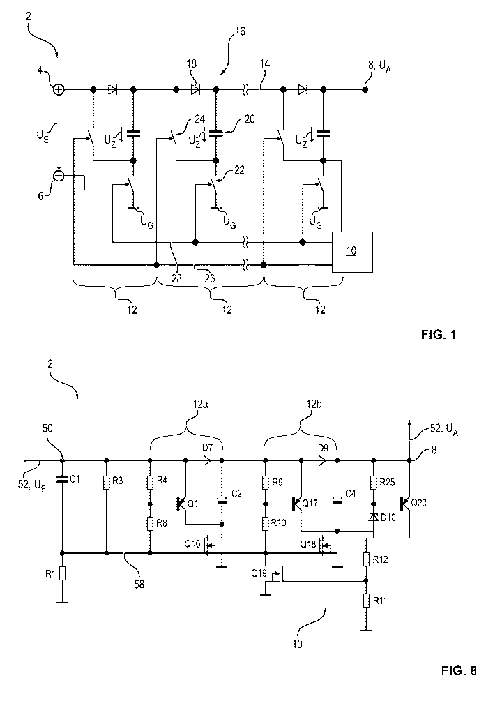
FIG. 1 schematically depicts a voltage multiplier 2 for converting an input
voltage UE into
an output voltage UA that is higher than the input voltage. The input voltage
UE is on the
input side between a first terminal connection or positive pole 4 and a second
terminal
connection or negative pole 6, and the output voltage UA may be tapped at a
tap point
8.
The voltage multiplier 2 has a control unit 10, for example in the form of a
controller.
The control unit 10 is connected for signaling purposes with a number of
voltage stages
12 that are connected in parallel between the terminal connections 4, 6 and
the tap
point 8. FIG. 1 shows three such voltage stages 12 by way of example.
A line 14 extends between the positive pole 4 and the tap point 8, and the
voltage
stages 12 are connected in parallel with each other along this line. Each
voltage stage
12 has a series circuit 16 wherein a rectifier diode 18 and a charging
capacitor 20 as
well as a switchable first semiconductor switch 22 are connected along the
line 14. In
other words, the rectifier diodes 18 of adjacent voltage stages 12 are
connected in
series with each other along the line 14. The series circuit 16 is led to a
reference-earth
8
,
CA 03053432 2019-08-13
potential UG, which in the exemplary embodiment of FIG. 1 is in particular a
ground
potential. A switchable second semiconductor switch 24 is connected to the
respective
voltage stage 12 parallel to the rectifier diode 18 and the charging capacitor
20. By way
of example, in FIG. 1 only the switching components for one voltage stage 12
are
assigned reference signs.
The semiconductor switches 22 of the voltage stages 12 may be gated by the
control
unit 10 by means of a first signal line 26. By means of a second signal line
28, the
semiconductor switches 24 are signal-connected to the control unit 10.
During operation, the voltage multiplier 2 is supplied with the input voltage
UE via the
terminal connections 4 and 6. The control unit 10 controls the semiconductor
switches
22 and 24 of the voltage stages 12 according to the below-described method
according
to the invention.
At the outset, the control unit 10 closes the semiconductor switches 22 by
means of the
signal line 26, while the control unit 10 gates open the semiconductor
switches 24 by
means of the signal line 24. In other words, the semiconductor switches 22 are
switched
to be conductive and the semiconductor switches 24 are switched to be
blocking. As a
result, the charging capacitors 20 of the voltage stages 12 along the line 14
are
respectively switched between the positive pole 4 and the reference-earth
potential UG.
As a result, the charging capacitors 20 of the voltage stages 12 are connected
in
parallel to each other, so that they are charged to a respective individual
voltage Uz via
the rectifier diodes 18.
During operation, the control unit 10 monitors the individual voltage Uz
(charging
voltage) generated at the charging capacitor 20 on the output side, i.e. at
the charging
capacitor 20 of the voltage stage 12 closest to the tap point 8. If this
individual voltage
Uz reaches or exceeds a preset or stored threshold voltage, the control unit
10 opens
the semiconductor switches 22 and closes the semiconductor switches 24. As a
result,
the charging capacitors 20 previously connected in parallel are now connected
in series
along the line 14. Thus, the output voltage UA at the tap point 8 is a sum of
the
individual voltages UZ of the charging capacitors 20. Depending on the number
of
voltage stages 12, it is possible to generate an output voltage UA that is
almost any
arbitrary multiple of the input voltage UE.
In the following, an example of the use of a or the voltage multiplier 2 in a
disconnecting
apparatus 30 is described in greater detail with reference to FIGS. 2 to 8.
9
CA 03053432 2019-08-13
FIG. 2 schematically depicts a disconnecting apparatus 30, which in this
exemplary
embodiment is connected between a DC source 32, specifically a photovoltaic
generator, and an electrical device 34, specifically an inverter. The
photovoltaic
generator 32 may comprise, in a manner and type not otherwise shown, a number
of
solar modules that are connected in parallel with each other to a shared
generator
connection box that serves as an energy collection point.
In a main current path 36 representing the positive pole, the disconnecting
apparatus 30
comprises a switching contact 38, hereinafter also referred to as a mechanical
switch,
and power electronics 40 connected in parallel therewith, as well as a pulse
generator
42 that gates the power electronics. The disconnecting apparatus 30 further
comprises
a protective circuit 44 and a power supply 46. The voltage multiplier 2 is
connected
between the power supply 46 and the pulse generator 42.
The mechanical switch 38 and the power electronics 40, together with the pulse
generator 42, form an autonomous hybrid disconnector (hybrid switch). An
additional
hybrid disconnector may be connected, in a manner not otherwise shown, on a
feedback line 48 representing the negative pole of the disconnecting apparatus
30 --
and thus of the entire system. Mechanically coupled switching contacts of an
additional
mechanical isolating element for complete galvanic isolation or DC
interruption between
the photovoltaic generator 32 and the inverter 34 may be arranged both in the
feed line
(main path) 36 representing the positive pole and in the feedback line 48, in
a manner
not otherwise shown.
If the current-carrying mechanical switch 38 is then opened during operation,
an arc LB
forms between its switching contacts. A capacitor C9 (FIGS. 3 and 7) is
charged as an
energy store, via the switch terminals J1 and J2 shown in FIG. 3, by means of
the
resulting arc voltage. The charging voltage of the capacitor C9 is fed to a
terminal
connection 50 of voltage multiplier 2 as the input voltage UE. By means of
this input
voltage UE, the voltage multiplier 2 generates an output voltage UA that is
higher than
the input voltage. As soon as the output voltage UA reaches a certain value,
the pulse
generator 42 gates the power electronics 40 so that they short-circuit the
switch 38 and
extinguish the arc LB.
In this case, the power electronics 40 suitably remain switched on for a
certain period of
time, i.e. for a timer period that is or may be set, so that the switching
path may be
deionized. After the time span or the corresponding timer period has elapsed,
the pulse
CA 03053432 2019-08-13
generator 42 switches off the power electronics 40. An overvoltage occurring
during the
switching process is limited by at least one varistor R5 (FIGS. 3 and 5). The
protective
circuit 44 monitors a respective power semiconductor (IGBT) T1, T2 of the
power
electronics 40 during the switching process in order to prevent it from being
destroyed
by an impermissibly high current.
FIG. 3 shows the disconnecting apparatus 30 in the detailed circuit diagram,
and the
different line types used in FIG. 2 frame the components of the power
electronics 40,
the pulse generator 42, the voltage multiplier 2, the protective circuit 44
and the power
supply 46. Because the power electronics 40 preferably have two semiconductor
switches in the form of the depicted IGBTs T1 and T2, two protective circuits
44 and two
driver circuits are respectively furnished for the IGBTs T1 and T2. For
reasons of clarity,
in this case, respectively only one of these circuits and the components
thereof is
bordered with the corresponding line type. The individual component circuits
are shown
separately in FIGS. 4 to 7.
According to FIGS. 3 and 4, the pulse generator 7 comprises a semiconductor
switch in
the form of a thyristor T4 connected to the capacitor C9 via a connection 52,
the
thyristor being connected on the anode side to the connection 52 leading to
the
capacitor C9 via a PMOS transistor (P-channel metal oxide semiconductor
transistor)
Q2, i.e. via the collector-emitter path thereof. The thyristor T4 is connected
on the gate
side via a PMOS transistor Q3 that is connected to resistors R16 and R17 and
to a
Zener diode D11. The thyristor T4 is connected on the cathode side to a
voltage tap 54
via a resistor R14, which is connected to ground via a resistor R15. In
addition, the
voltage tap 54 is connected to ground (reference-earth potential) via the
drain-source
path of another transistor Q4, here a MOS or NMOS transistor. The voltage tap
54 also
houses the base or gate of another transistor (MOS or NMOS transistor) Q5, the
drain-
source path of which is connected via resistors R19, R20 as variable resistor
and R21
and a capacitor C3 connected in parallel to resistor R19 between the
connection 52
leading to capacitor C9 and the ground.
Parallel to the RC element R19 and C3 there is a series circuit consisting of
a resistor
R23 and a Zener diode D12, to which the base of a PNP transistor Q7 is
connected on
the cathode side. The gate side of an additional thyristor T5 is connected via
the
transistor Q7 and a resistor R24 to the connection 52 that connects to the
capacitor C9.
The anode-cathode path of the thyristor T5 is connected between the connection
52
leading to the capacitor C9 and -- via a resistor R22 -- to ground. A cathode
side tap of
this thyristor T5 is connected to the gate (base) of the transistor Q4 via a
resistor R18
and to the gate (base) of the transistor Q2 via a resistor R13. In addition to
the
semiconductor switch T4, the circuit shown and described represents an
appropriately
11
CA 03053432 2019-08-13
wired semiconductor circuit of the pulse generator 42. The pulse generator 42
generates the or each control pulse P for the two IGBTs Ti, T2 of the power
electronics
6, as explained below.
The two thyristors 14 and 15 of the pulse generator 42 are in the blocking
state at the
beginning, and thus the gate of the transistor Q2 is at ground potential. If,
as a result of
an arc LB generated when the mechanical switch 5 is opened, the charging
voltage of
the capacitor C5 arising due to the output voltage of the voltage multiplier 2
and thus the
operating voltage rises, then the negative gate source voltage of the
transistor Q2 will
also rise so that the transistor switches through and the anode of the
thyristor 14 has
the potential of the operating voltage. If this voltage rises further, the
Zener diode D1
begins to transition to the conductive state. The resulting current flow
causes a voltage
drop at resistor R17. If this voltage drop exceeds the threshold value of the
base-emitter
voltage of the transistor 03, it becomes conductive. To protect the transistor
Q3 from
destruction, the current is limited by the resistor R16. This current causes
the thyristor
14 to fire. The value of the resistor R14 is substantially smaller than that
of the resistor
R15, so that the potential between these two resistors R14, R15 at the voltage
tap 54 at
which the control pulse P for the power electronics 6 is tapped, is only
slightly below the
operating voltage.
As soon as the thyristor T4 has fired, the transistor Q5 switches through and
the
capacitor C3 is charged via the resistors R20 and R21. Because the capacitor
C3 is
initially uncharged, the potential of the anode of the Zener diode D12 is at
the operating
voltage. As a result of the capacitor C3 charging, the potential shifts to
ground. If this
potential has dropped to such an extent that the Zener diode D12 becomes
conductive,
a current flows through resistor R23. If the voltage drop across resistor R23
exceeds the
threshold base-emitter voltage of the PNP transistor 07, that transistor
switches
through. The resistor R24 here limits the current and protects the transistor
07.
The current flowing through the transistor Q7 causes the thyristor 15 to fire,
so that the
potential at the thyristor's cathode rises to the operating voltage -- minus
the forward
voltage. Thus the transistor Q4 also switches through and drops the potential
between
the resistors R14 and R15 at the voltage tap Si to ground. In addition, the
transistor Q2
now blocks, eliminating the thyristor 14. The transistor Q5 then also blocks,
and the
capacitor C3 is discharged via the resistor R19. The thyristor 15 remains
conductive
until the capacitor C9 is discharged. Because the capacitor C9 is recharged
during a
light ground phase and also during the switching overvoltage, only a single
control pulse
is triggered. The power electronics 40 shown in FIGS. 3 and 5 are associated
with a
driver stage 56. The IGBTs Ti and T2 of the power electronics 40 form the
lower part of
a B2 rectifier bridge. By using two power semiconductors with a free-wheeling
diode in
12
CA 03053432 2019-08-13
the form of the IGBTs T1 and T2, a bidirectionally-capable circuit is
achieved. If the
illustrated switch or contact terminal J2 of the mechanical switch 38 has a
positive
potential and the other switch terminal J1 has a negative potential, the
current may flow
through the IGBT T2 and the free-wheeling diode of the IGBT Ti. If the
polarity is
reversed, current may flow through the IGBT T1 and the free-wheeling diode of
the
IGBT T2. Because the control signal of an IGBT has no influence on its inverse
operation, both 1GBTs T1 and T2 of the power electronics 40 are always
controlled.
Because the driver circuits 56 of both IGBTs T1 and 12 are identical, only one
of the
two driver circuits 56 is described below. The driver circuit 56 comprises an
NPN
transistor Q8 and a PNP transistor Q6, which are connected to a complementary
output
stage. If the pulse generator 42 sends the control pulse P to the bases of the
two
transistors Q6 and Q8, these transistors act as current amplifiers and enable
rapid
recharging of the gate of the respective IGBT T2, Ti. As a result, a
particularly fast
switching process is achieved. A capacitor C5 of the driver circuit 56
provides the
recharging current. The IGBT T2 is damped by a resistor R28, because parasitic
inductances and capacitances may cause oscillations during gating of the
respective
IGBT T2. A Zener diode D16 of the driver circuit 11 protects the gate of the
IGBT 12
against overvoltages, in the event that fluctuations nonetheless occur.
Because
overvoltages may occur when switching inductive loads due to the steep
switching edge
of the IGBT T2, the varistor R5 limits the overvoltage to prevent destruction
of the power
semiconductors T1 and T2.
FIGS. 3 and 6 show the measuring and protection circuit 44 of the
disconnecting
apparatus 30. Although IGBTs, as semiconductor switches of the power
electronics 40,
are in principle short-circuit-proof, in the event of a fault they must
nonetheless be
switched off within 10 ps. The circuits 44 for monitoring or measuring the
current of the
two IGBTs 11, 12 are identically constructed, so FIG. 6 shows only one such
circuit 44.
The measuring circuit substantially comprises a series circuit of a resistor
R27 and a
diode D3, which is/are connected between the gate and the collector of the
IGBT T2.
The control signal of the IGBT 12 is fed to its collector-emitter path via the
resistor R27
and the diode D3.
The potential between the diode D3 and the resistor R27 corresponds to the
forward
voltage of the IGBT 12, plus the saturation voltage of the diode D3. Thus,
based on the
IGBT characteristic, the current flow through this power semiconductor T2 may
be
determined. The resistor R27 is relatively high-impedance so as not to
unnecessarily
strongly discharge the capacitor C9, which serves as an energy store, during
the
switching phase. In order to nonetheless enable rapid switch-off in the event
of a fault, a
complementary output stage with correspondingly connected transistors Q11 and
Q12
13
CA 03053432 2019-08-13
is connected downstream. A diode D14 connected to the output stage on the
emitter
side enables the parallel connection of the two measuring circuits D3, R27 and
D4, R28
(FIG. 3).
A thyristor T6 of the protective circuit 44 will fire if the collector-emitter
voltage of the
IGBT 12 exceeds a specified potential. As a result, the transistor Q7 of the
pulse
generator (pulse generator circuit) 42 is then activated, initiating the
switch-off process.
A capacitor C7 connected to ground on the gate side of the thyristor 16, and a
resistor
R31 connected in parallel to this capacitor, form a filter to prevent, among
other things,
tripping of the protective circuit 44 during the switch-on phase of the IGBT
T2. The
tripping voltage may be ascertained by the following formula.
UcE(T2) UBE(Q12) + UD(D14) + Uz(D13) + U(T6) ¨ UD(D3),
where UCE is the collector-emitter voltage, UBE is the base-emitter voltage,
UD is the
forward voltage, Uz is the Zener voltage and Uzu is the firing voltage. FIGS.
3 and 7
show the circuit design of the power supply 46 of the disconnecting apparatus
30. The
power supply 46 is used to charge the capacitor C9 as an energy store and to
protect
against a switching overvoltage. The mechanical switch 38 is located between
the
switch or contact connections J1 and J2 (FIG. 2). As soon as the switch 38
opens the
circuit, the arc LB forms. The arc voltage is rectified via diodes D1, D2
connected in
current paths 40a and 6b of the semiconductor switches (power switches) T1 and
12 of
the power electronics 40 and the free-wheeling diodes of the IGBTs T1 and 12.
The power supply 46 comprises a semiconductor switch in the form of an IGBT
T7, the
gate of which is charged via resistors R33 to R37. As soon as the gate-emitter
potential
of the thyristor T7 exceeds the threshold voltage, the IGBT 17 activates and
the
capacitor C9 is charged. An NPN transistor Q15 is connected to the IGBT 17 in
the
manner shown in FIG. 7. On the emitter side, the transistor Q15 is connected
to ground
via a Zener diode D19. If the potential of the capacitor C9 reaches the value
of the
Zener diode D19 plus the base-emitter threshold voltage of the transistor Q15,
it
becomes conductive and limits the gate-emitter voltage of the IGBT 17. This
IGBT then
begins to block, and the charging current of the capacitor C9 is interrupted.
To protect
the gate of the IGBT 17 and the transistor Q15 from overvoltage, a Zener diode
D19 is
inserted on the base gate side of the semiconductor switches 17 and Q15.
In order to reduce the switching delay time for short-circuiting the switching
path or for
extinguishing the arc LB, the voltage multiplier 2 shown in FIG. 8 is
connected
downstream of the power supply 46 in the connection 52. With the voltage
multiplier 2 it
14
CA 03053432 2019-08-13
is possible, for example, to convert a 5 V supply or input voltage, which is
not sufficient
to generate a control pulse P by means of which the IGBTs Ti and 12 may be
securely
controlled, into an output voltage of 15 V -- which enables the IGBTs Ti and
T2 to be
securely controlled.
The voltage multiplier 2 is connected between the terminal connection 50 and
the tap
point 8 in the connection 52, and in this embodiment has two voltage stages
12a and
12b. A capacitor Cl of the control unit 10 is connected to the terminal
connection 50,
which is connected to ground (reference-earth potential) by means of a
resistor R1. In
this embodiment, the control unit 10 is implemented purely as circuitry. For
this purpose,
between the capacitor C1 and the resistor R1 a signal connection 58 is made,
by means
of which the voltage stages 12a and 12b may be controlled. A resistor R3 is
connected
between the connections 52 and 58, in parallel with the capacitor C1.
The voltage stage 12a comprises a (rectifier) diode D7, which is connected to
ground in
series with a (charging) capacitor C2 and with a transistor Q16 implemented as
MOS-
FET. A bipolar PNP transistor Q1 is connected in parallel with the diode D7
and the
capacitor C2 and is connected on the gate side to a tap point of a voltage
divider 60a
which is formed by the resistors R4 and R8 connected between the connections
52 and
58.
Correspondingly, the voltage stage 12b has a series circuit made up of a diode
D9, a
capacitor C4 and a transistor Q18. A transistor Q17 is connected in parallel
to the diode
D9 and the capacitor C4, and is gated by two resistors R9 and R10 as a voltage
divider
60b.
In this exemplary embodiment, the control unit 10 comprises a resistor R25 and
a Zener
diode D10 that are connected in parallel to the capacitor C4 in the manner
shown in
FIG. 8. Between the Zener diode D10 and the resistor R25, the control input of
a bipolar
PNP transistor Q20 is connected, which is connected to ground on the emitter
side at
the tap point 8 and to ground on the collector side by means of two resistors
R12 and
R11. A gate terminal of a transistor Q19, implemented as MOS-FET, is connected
between the resistors R12 and R11. The transistor Q19 is connected to ground
on the
source side and is connected to the signal line 58 via the drain terminal; the
drain
terminal is connected between the gate terminal of the transistor Q18 and the
source
terminal of the transistor 16 [sic]. Initially, the capacitors Cl and C2 as
well as C4 are
uncharged and the transistors Q16 and Q18 as well as Q1 [sic] and Q17 are in
an
electrically non-conductive state. If an input voltage is applied to the
terminal connection
50 by the power supply 46, a current flows through the capacitor Cl. As a
result, the
CA 03053432 2019-08-13
gates of the transistors Q16 and Q18 are charged. The transistors Q16 and Q18
then
switch through, charging the capacitor C2 via the diode D7 and the capacitor
C4 via the
diodes D7 and D9, with a respective individual voltage.
If the individual voltage or charging voltage of the capacitor C4 of the
voltage stage 12b
reaches a given value, the Zener diode D10 enables a current flow through the
resistor
R25. If the voltage drop across resistor R25 rises to, for example, 0.7 V, the
Q20
transistor switches through. As a result, a voltage is applied to the gate of
the transistor
019, which is limited by the voltage divider formed by the resistors R12 and
R11. The
transistor Q19 then switches through and pulls the gates of the transistors
Q16 and 018
to ground, so that these transistors are blocked and the charging process of
the
capacitors C2 and C4 is terminated.
As a result of the transistor Q19 being switched through, an electric current
flows
through the series circuits of the resistors R4 and R8 as well as the
resistors R9 and
R10, or through the voltage dividers 60a and 60b. Due to the voltage drops
across
resistors R4 and R9, PNP transistors 01 and Q17 are switched through. The
diodes D7
and D9 prevent discharge of the capacitors C2 and C4. Thus the capacitors C2
and C4
are effectively connected in series along the connection 52. This generates an
output
voltage at the tap point 8 that consists of the input voltage at the terminal
connection 50
plus the charging or individual voltages of the capacitors C2 and C4.
The invention is not limited to the exemplary embodiments described above.
Rather,
other variants of the invention may also be derived from it by the skilled
person without
departing from the subject matter of the invention. In particular, all the
individual
features described in connection with the exemplary embodiments may also be
combined together in other ways without departing from the subject matter of
the
invention.
16
CA 03053432 2019-08-13
List of Reference Signs
2 Voltage multiplier
4 Terminal connection / positive pole
6 Terminal connection / negative pole
8 Tap point
Control unit
12, 12a, 12b Voltage stage
14 Line
16 Series circuit
18 Rectifier diode
Charging capacitor
22, 24 Semiconductor switches
26, 28 Signal line
Disconnecting apparatus
32 DC source / photovoltaic generator
34 Device / inverter
36 Main current path
38 Switch contact / switch
Power electronics
42 Pulse generator
44 Protective circuit
46 Power supply
48 Feedback line
Terminal connection
52 Connection
54 Voltage tap
56 Driver stage
58 Signal connection
17
CA 03053432 2019-08-13
60a, 60b Voltage divider
UE Input voltage
UA Output voltage
UG Reference-earth potential
Uz Individual voltage
LB Electric arc
J1, J2 Switch connection
Control pulse
18