Note: Descriptions are shown in the official language in which they were submitted.
CA 03055719 2019-09-06
WO 2017/155801
PCT/US2017/020576
SYSTEM AND METHOD FOR FABRICATING AN ELECTRODE
WITH SEPARATOR
CROSS-REFERENCE TO RELATED APPLICATION
[0001] The
present application a continuation-in-part of, and claims priority to, U.S.
Patent Application Serial No. 13/617,162, filed September 14, 2012, which is a
non-
provisional of, and claims priority to, U.S. Provisional Application
61/647,773 filed
May 16, 2012, the disclosures of which are incorporated herein in their
entirety.
GOVERNMENT RIGHTS IN THE INVENTION
[0002] The U.S.
Government has a paid-up license in this invention and the right in
limited circumstances to require the patent owner to license others on
reasonable terms
as provided for by the terms of 5P4701-09-D-0049 CLIN 0002 and HQ0147-140-C-
8307 awarded by Defense Logistics Agency.
BACKGROUND OF THE INVENTION
[0003]
Embodiments of the invention relate generally to a dry, solvent-free method
and apparatus for fabricating electrodes and, more particularly, to a method
and
apparatus for forming separator layer on an electrode.
[0004]
Typically, power sources, such as batteries, capacitors and fuel cells contain
a
positive and negative electrode. Depending on the chemistry of the power
source,
manufacturing methods vary. Many methods, such as those used in the Li-ion
industry,
include mixing active materials, conductive materials and binders in a wet
slurry, using
a solvent, and applying to a substrate. The application may be via doctor
blade, roll
transfer coating, slot die or extrusion.
[0005] The cast
electrodes are then dried in ovens, while the solvent is recaptured so
as not to allow fumes to escape into the environment, or the solvent is used
as
supplemental fuel for the drier. This process is time-consuming and expensive.
The
ovens are usually very large, long, expensive and space-consuming as well. The
solvents are typically flammable, hard to remove from the chemical structure,
bad for
the environment, and costly to handle correctly, both environmentally and from
a safety
1
CA 03055719 2019-09-06
WO 2017/155801
PCT/US2017/020576
perspective. If solvent recovery is desired the solvent needs to be captured,
condensed,
cleaned and prepared for reuse or disposal.
[0006] Some known methods of power source manufacturing have moved away
from solvent slurries on one electrode, but typically still use a solvent-
based method on
the other electrode. The non-solvent method usually includes pressing or
extruding a
mix of active materials, conductive materials and binder into an electrode,
which then is
attached to a substrate or current collector. Present day manufacturing
techniques
therefore limit throughputs, and the cost of such electrodes can be excessive.
[0007] The
electrodes made through the solvent casting and subsequent extraction
typically exhibit good adhesion to the current collector when the dried
electrode is
mechanically coined. The act of solvent casting and subsequent extraction
leaves the
binder and electrode structure open, similar to that of a sponge structure.
The coining
operation crushes the electrode structure back down leaving a porosity of 30
to 50%.
Upon wetting with the electrolyte this crushed sponge-like structure relaxes
and exhibits
what is commonly referred to as swelling of the electrode. The typical anode
binder,
known as PVDF-Polyvinylidene fluoride or polyvinylidene difluoride (PVDF), is
a
highly non-reactive and pure thermoplastic fluoropolymer produced by the
polymerization of vinylidene difluoride. It is one of the few known binders
that do not
readily react at the lithium potential of the anode and thus is typically
preferred as a
binder in Li-ion batteries.
[0008] Some manufactures have tried to develop processes using
polytetrafluoroethylene (PTFE) and fibrillating the binder as to create a free
standing
film. This active material loaded free standing film is then pressed onto a
current
collector to be made into an electrode. PTFE is not stable at the Lithium ion
anode
potential so its use is limited to that of a cathode binder. Other
manufacturers have tried
to use water based binders to create the lithium electrode structure. They
have difficulty
with drying the electrode thoroughly to prevent the moisture reacting with the
lithium
salts, detrimentally affecting the performance of the resulting battery.
2
CA 03055719 2019-09-06
WO 2017/155801
PCT/US2017/020576
[0009] Thus,
the preferred method of fabricating Li-ion batteries typically includes a
solvent-based method, for at least one electrode, that meet demanding
performance
requirements, while also meeting demanding and rigorous life requirements (by
exhibiting adequate adhesion to the base material). However, because of the
costs
associated with handling, reclaiming, and ultimately disposing of these
environmentally
challenging solvents, the cost of manufacturing Li-ion and other solvent-based
electrodes can be excessive.
[0010] Battery
fabrication also includes application of a battery separator to
electrodes of the battery, with the battery separator being placed between
a battery's anode and cathode to keep the two electrodes apart to prevent
electrical short
circuits while also allowing the transport of ionic charge carriers that are
needed to close
the circuit during the passage of current in an electrochemical cell. It is
recognized that
numerous drawbacks are associated with existing battery separator fabrication
and
application methods. That is, for batteries with a small cell area and a large
number of
stacked electrodes, challenges arise with respect to alignment and stacking
during
assembly, as well as shorting issues, therefore causing overall cell yield to
be lower.
Tabbing of individual electrodes and separator placement present challenges in
manufacturing the battery, with techniques such as heat staking the separator
on the
edges of the electrode being helpful but not fully addressing the challenge of
overall
alignment and shorting.
[0011] In a
typical battery separator fabrication and application method, the battery
separator is formed as a stand-alone sheet/layer that is formed via mixture of
a separator
material with pour-forming oil and a subsequent blow, cast, and
extraction/calendaring
process to leave the separator as a micro-porous body. A ceramic separator
uses a
polyolefin base material with ceramic particles added to the base material to
result in a
high polymer (15-35%) loaded ceramic separator. The separator material is
stored on a
roll and subsequently requires further slitting and cutting-to-size to produce
a separator
for each specific cell and battery type, with the slit/cut separator then
being aligned and
applied to the cell/battery during the actual manufacturing thereof.
3
CA 03055719 2019-09-06
WO 2017/155801
PCT/US2017/020576
[0012]
Therefore, it would be desirable to provide a solvent-free method and
apparatus for fabricating electrodes. It would also be desirable for provide a
method for
applying a separator directly to the electrodes, so as to eliminate additional
slitting,
cutting-to-size and alignment steps associated with separator preparation and
application.
4
CA 03055719 2019-09-06
WO 2017/155801
PCT/US2017/020576
BRIEF DESCRIPTION OF THE INVENTION
[0013] The
invention is a directed method and apparatus for fabricating electrodes
and, more particularly, for forming ceramic-based separators for electrodes.
[0014]
According to one aspect of the invention, a method of applying a dry,
solvent-free ceramic-based separator to an electrode includes providing an
electrode to
an application area via a feed mechanism and applying a separator layer
comprised of a
binder and an electrically non-conductive separator material to the electrode
via a dry
dispersion application, wherein the binder includes at least one of a
thermoplastic
material and a thermoset material.
[0015]
According to another aspect of the invention, a method of manufacturing a
battery cell that includes an electrode and a separator includes providing an
electrode,
advancing the electrode toward an application region, and coating a mixture of
an
electrically non-conductive ceramic-based separator material and a binder onto
the
electrode in the application region via a dry, solvent-free coating process,
so as to form
a separator layer.
[0016]
According to yet another aspect of the invention, a battery cell includes an
electrode and a separator layer adhered to the electrode, the separator layer
comprising a
binder comprising at least one of a thermoplastic material and a thermoset
material and
an electrically non-conductive ceramic-based separator material, wherein the
separator
layer ranges from 2-30% binder by weight.
[0017] Various
other features and advantages will be made apparent from the
following detailed description and the drawings.
CA 03055719 2019-09-06
WO 2017/155801
PCT/US2017/020576
BRIEF DESCRIPTION OF THE DRAWINGS
[0018] The drawings illustrate preferred embodiments presently contemplated
for
carrying out the invention.
[0019] In the drawings:
[0020] FIG. 1 illustrates components of a system for forming active
electrode
materials on an electrode substrate, according to an embodiment of the
invention.
[0021] FIG. 2 illustrates steps for applying a base layer to an electrode
substrate and
one or more electrode layers of active material thereto according to
embodiments of the
invention.
[0022] FIG. 3 illustrates a base layer having an electrode formed thereon
using an
embodiment of the invention.
[0023] FIG. 4 illustrates components of a system for forming active
electrode
materials on two sides of an electrode substrate, according to an embodiment
of the
invention.
[0024] FIG. 5 illustrates a base layer having an electrode formed on two
sides of an
electrode substrate using embodiments of the invention.
[0025] FIG. 6 illustrates components of a separator system for applying a
separator
layer to an electrode, with the separator system being integrated with the
system of FIG.
1, according to an embodiment of the invention.
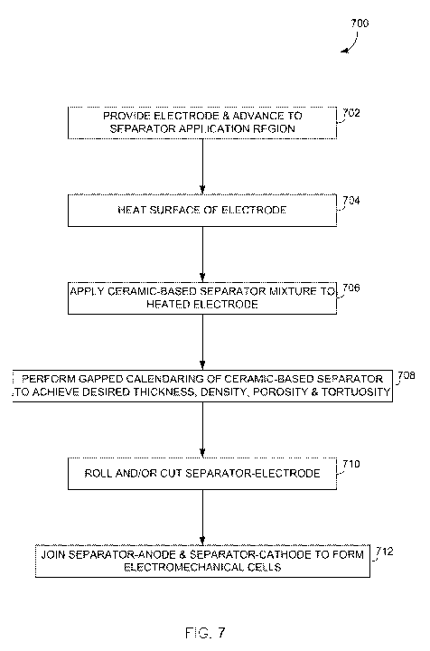
[0026] FIG. 7 illustrates a dry, solvent-free method for applying a battery
separator
onto an electrode, according to an embodiment of the invention.
[0027] FIG. 8 illustrates an electrochemical cell resulting from combining
an anode-
separator structure and a cathode-separator structure, according to an
embodiment of the
invention.
6
CA 03055719 2019-09-06
WO 2017/155801
PCT/US2017/020576
DETAILED DESCRIPTION
[0028]
According to embodiments of the invention, electrodes for energy storage
devices, such as lithium ion batteries, are fabricated using a solvent-free
method and
apparatus, and a separator layer is applied to the electrodes via a dry
dispersion process.
[0029] FIG. 1
illustrates a system 100 for fabricating electrodes by depositing binder
and active electrode material on one side of a substrate 102 (otherwise known
as a
current collector in a finished electrode). The substrate 102 can include in
one example
copper as an anode current collector or aluminum as a cathode current
collector. In
another example, the anode current collector is a composite that includes for
instance
steel. As other examples, substrate 102 could also include but is not limited
to a nickel
plated steel, a composite of fibrous carbon, a tin dioxide (5n02), and could
be for
instance a punched solid sheet or an expanded composite (i.e., having
perforations that
allow for an open expansion of the substrate to reduce weight or allow higher
mechanical or material loading). However, the invention is not so limited and
any
substrate or collector material may be used to form an electrode having other
active
material(s), according to what is known in the art. The active material or
active material
mixture includes but is not limited to lithium titanate oxide (LTO), cobalt
oxide, nickel
oxide, manganese oxide, nickel cobalt manganese oxide, iron phosphate, iron
oxide,
carbon, and silicon.
[0030]
Substrate 102 is fed through a feed mechanism or roller system 104 having a
feed mandrel 106 that provides material for substrate 102 and which is guided
by
oppositely rotating guide mandrels 108. In embodiments of the invention,
substrate 102
may be a single sheet of electrode, or may be a continuous feed thereof
Substrate 102
is fed through a first application region 110 and through a second application
region 112
during which time mixes that may include binder, active material, and
conductive
material are applied or otherwise sprayed onto substrate 102. Heat is applied
within
application regions 110, 112, and/or after passing therethrough as will be
further
described, in order to effect binding and formation of electrode materials.
Substrate is
passed through a second set of guide mandrels 114 that guide the substrate,
having
active electrode material bound thereto, toward a collection mandrel 116.
According to
7
CA 03055719 2019-09-06
WO 2017/155801
PCT/US2017/020576
the invention, second set of guide mandrels 114 may be designed having a space
or gap
therebetween that is maintained during operation in order to compress
substrate 102
having the electrode thereon to a final desired and consistent thickness.
[0031] First
application region 110 includes a device 118 for applying a first layer to
substrate 102 that includes a spray mechanism (such as a spray gun or other
known
devices for causing a spray) that is configured to spray 120 a first or base
layer of a mix
of material onto substrate 102. In general, although first application region
110 is
described as having a spray mechanism or gun in order to apply material onto
the
substrate, and such is illustrated as "spray 120", it is contemplated that any
mechanism
may be used to apply the material, to include painting, brushing, powder
coating, using
a fluidized bed, doctor blading, or wiping with a rag, as examples. In fact,
in this and
all subsequent application regions described, it is contemplated that a spray
gun or other
known spray device may be employed for applying first and subsequent layers to
the
substrate 102, or any mechanism may be used to apply the materials, as
described
above, and that the term "spray" may be applied to any mechanism or means that
are
used to apply a liquid to a surface.
[0032]
According to the invention, device or spray mechanism 118 causes spray 120
to emit between approximately 2 and 20 psi. According to the invention, spray
120
includes a mix of binder, conductive carbon, and active electrode material.
The binder,
according to one embodiment, includes a thermoplastic or a thermoset material,
which
in one embodiment is polyvinylidene fluoride (PVDF) ranging between 6 ¨ 85% by
weight of the total material in spray 120. However the invention is not to be
so limited,
and for instance binder levels as low as 1% or as high as 100% may be used.
Further,
the invention is not limited to PVDF, but may include any binder that is known
within
the art that include, according to embodiments of the invention and as stated,
thermoplastics and thermoset materials. As known in the art, thermoplastics
are a
polymer that becomes pliable above a certain temperature, and returns to a
solid stated
upon cooling. In contrast and as also known in the art, a thermoset material
forms an
irreversible chemical bond during the curing process, which breaks down upon
melting
(and does not reform upon cooling). According to embodiments of the invention,
the
8
CA 03055719 2019-09-06
WO 2017/155801
PCT/US2017/020576
binder may be PVDF or any derivative thereof, or PTFE or any derivative
thereof, as
examples. According to another embodiment of the invention, a very high
molecular
weight polyethylene material may be included in the binder to add structural
integrity to
the binder. The conductive carbon, as known in the art, may be included in
order to
cause or enhance electrical contact between particles within the electrode.
[0033] Spray
120 may also includes generally 4 ¨ 8% conductive carbon to include a
graphite such as TIMREX K56 (TIMREX is a registered trademark of Timcal SA of
Switzerland) (although increased amounts of conductive carbon to 17% or higher
and
up to, for instance, 40% may be used, according to the invention). The balance
% of
spray 120 is active electrode materials which include but are not limited to
LTO, cobalt
oxide, nickel oxide, manganese oxide, nickel cobalt manganese oxide, iron
phosphate,
iron oxide, carbon, and silicon. As one example, spray 120 includes 13% binder
and
8% conductive carbon, and the balance of spray 120 is 79% active material, by
weight.
[0034]
According to the invention, spray 120 deposited upon substrate 102 within
first application region 110 is heated in order to initiate binding of the
first layer mix to
substrate 102. In one embodiment, a heater 122 is positioned opposite device
118 and
adequate power is provided to heater 122 to raise the temperature of substrate
to
between approximately 100 F and 500 F, and in one embodiment to 300 F.
However,
in another embodiment, a heater 124 is positioned to heat a surface of
substrate 102
opposite a surface of substrate 102 to which spray 120 is applied. In this
embodiment
as well, heater 124 is powered to raise the temperature of substrate to
between
approximately 100 F and 500 F, and in one embodiment to 300 F. Heat may also
be
applied, in one embodiment, via a heater 126 to the base layer after passing
through first
application region 110 at least until the first layer reaches a plastic state,
after which the
first layer may be allowed to cool prior to applying a subsequent layer of
electrode
material. Thus, according to the invention, a first layer or base layer of
electrode
material is applied to substrate 102 and binding thereto is initiated via one
or both
heaters 122, 124. The binder of base layer may also be melted throughout using
heater
126 in order to cause the base layer to melt and uniformly form on substrate
102.
Heaters 122, 124, and 126 may apply heat through any number of known
mechanisms.
9
CA 03055719 2019-09-06
WO 2017/155801
PCT/US2017/020576
For instance, heaters 122 - 126 may include infrared (IR) heaters, convective
heaters,
conductive heaters, radiant heaters (for instance, outside the IR spectrum),
or induction
heaters, as examples.
[0035] Heaters
122/124 and heater 126 generally serve different purposes. For
instance, heaters 122/124 provide heat that is directed toward the substrate
102 in order
that the binder material in contact with substrate 102 is caused to change to
a plastic
state (but not heated to the point that the binder readily melts and flows) to
adhere to
substrate 102. Heater 126, on the other hand, is generally directed toward
heating the
bulk of the sprayed material that forms the base layer. In such fashion,
according to the
invention, heat may be provided to either side of substrate 102, and heaters
122 and 124
may be provided at different locations relative to device 118, depending on
such factors
as the amount of binder in spray 120. Thus, different types of heaters may be
used for
the different desired type of heating to be performed. For instance, heaters
122 and/or
124 may be induction heaters that cause primarily substrate 102 to heat, while
heater
126 may be an IR, convective, or radiant heater. In another example, one or
all heaters
(122 and/or 124 and 126) are IR heaters. In fact, any combination of heaters
may be
used, according to the invention, depending on the desired type of heating to
be
performed (substrate versus a layer of applied material)
[0036] As known
in the art, it is generally desired to maximize the amount of active
material within the electrode. Thus, it is also desired to minimize the amount
of binder
used in spray 120, however under the constraining guideline that adequate
binding be
obtained in the base layer sprayed onto substrate 102 in first application
region 110.
Binding of the first layer of sprayed material 120 is affected by not only the
types of
heaters, temperatures obtained, and the like, but also by the amount of
binder,
conductive carbon, and active material present in spray 120. As known in the
art,
particle size may be actively selected based on the type of electrode to be
formed, and
may range from as low as nanometer-sized particles to hundreds of microns and
greater.
Particle size may also be varied throughout the depth of the electrode. As
such, particle
size of the active material influences not only the amount of active material
that may be
CA 03055719 2019-09-06
WO 2017/155801
PCT/US2017/020576
deposited in the base layer, but the amount of binder as well and the amount
of heat
applied to initiate binding of the base layer.
[0037]
According to the invention, device 118 may include a spray gun having an
electrostatic charge applied thereto in order to guide and accelerate
particles in spray
120 toward substrate 102. Known spray mechanisms include an electrostatic
charge
that is applied typically proximate a nozzle 128 of the spray gun 118 in order
that the
particles emitting from nozzle 128 are imparted with the charge, causing an
electrostatic
voltage differential to form between nozzle 128 and substrate 102. According
to one
embodiment, the electrostatic voltage applied to nozzle 128 is 25 kV, however
the
invention is not to be so limited and any voltage above or below 25 kV may be
applied,
such as 100 kV, according to the invention, in order that spray 120 is
uniformly applied
to substrate 102. The voltage differential may be enhanced by grounding a
region of
substrate 102 toward which spray 120 is directed. Because substrate 102 is
caused to
pass continuously through first application region 110, it may be inconvenient
to
directly ground substrate 102. Thus, according to the invention, a support
structure 130
may be provided over which substrate 102 passes. Support structure 130 is
stationary
and in electrical contact with substrate 102, thus grounding of substrate 102
may be
effected by providing a ground line 132 that is attached to support structure
130.
According to one embodiment, multiple ground lines may be included
(represented by a
second ground line 134, but many may be included according to the invention)
in order
to more uniformly ground substrate 102 proximate where spray 120 impinges
thereon.
[0038] System
100 includes second application region 112 which causes a second
layer to be deposited onto substrate 102. Second application region 112
includes a
device 136 (such as a spray gun or other known devices for causing a spray, as
described) that causes spray 138 to emit toward substrate 102 and land or
impinge on
the first layer applied in first application region 110. Because adhesion from
one
electrode layer to the next tends to be easier to achieve compared to the
initial base layer
to substrate 102, spray 138 for the second and any subsequent electrode layers
typically
includes less binder. Thus, according to one embodiment of the invention,
spray 138
includes 80 ¨ 90% active material by weight (including but not limited to LTO,
cobalt
11
CA 03055719 2019-09-06
WO 2017/155801
PCT/US2017/020576
oxide, nickel oxide, manganese oxide, nickel cobalt manganese oxide, iron
phosphate,
iron oxide, carbon, and silicon), 4 ¨ 8% conductive carbon by weight, and the
balance
as binder (PVDF in one embodiment). However the invention is not to be so
limited,
and for instance binder levels in the second electrode layer (and any
subsequent layers)
as well can be as low as 1% or as high as 100%. In fact, any composition and
percentage thereof of active material and binder may be included, according to
the
invention, in the first layer and in the second and subsequent layers applied
thereto.
[0039]
According to the invention one or both heaters 140 may be included that
provide heat to substrate 102. However, because substrate 102 already has a
base layer
thereon from first application region 110, heaters 140 may not be necessary as
the base
layer also provides a thermally insulating barrier to be formed. Also, heaters
140 may
not be included because binding from one electrode layer to the next can be
more
effective and heat from a heater 142 may be adequate to cause the subsequent
electrode
material from spray 138 to reach a plastic state.
[0040] Heaters 140 (if used) and 142 may provide heat from any number of known
methods, to include IR heaters, convective heaters, radiant heaters, or
induction heaters,
as examples. Further, device 136 may also include spray mechanism having a
nozzle
144 to which an electrostatic charge may be applied as well, such as 25 kV.
Application
region 112 may include a support 146 and one or more ground lines 148 for
enhancing
the deposition of spray 138 onto the base layer previously applied.
[0041]
According to the invention, system 100 includes a computer 150 with a
computer readable storage medium and having stored thereon a computer program
comprising instructions to execute control commands via a controller 152. In
such
fashion, controller 152 can be caused to control operation of the spray
stations, heaters,
and roller mechanism as known in the art and as described according to the
operation
above.
[0042] The
operation of system 100 of FIG. 1 can be summarized in a set of steps
within a block diagram 200 as illustrated in FIG. 2. Starting at step 202, a
substrate
material is fed 204 and a first layer or base layer of binder, conductive
carbon, and
12
CA 03055719 2019-09-06
WO 2017/155801
PCT/US2017/020576
active material is applied onto the substrate at step 206. Heat is applied to
the non-
sprayed side of the substrate at step 208 and, as stated, may include a heater
immediately opposite the location of the spray at step 206 and simultaneous
therewith,
and/or heat may be applied to the non-sprayed side of the substrate after the
substrate is
caused to pass through a region or zone where the base layer is applied. The
spray side
may then be heated at step 210 after which a first layer is formed on the
substrate. A
second layer of binder, conductive carbon, and active material is sprayed onto
the first
layer at step 212. As stated, the non-spray side may be heated 214 with
heaters
immediately opposite the second spray region, or subsequent thereto as
represented by
heaters 140 of FIG. 1. Heat may also be applied to the spray side 216 in order
to cause
the binder of the second layer to reach a plastic state/condition. As alluded
to,
subsequent layers may be applied to the electrode layers by repeating the
process
described. That is, referring to FIG. 1, additional spray stations such as
second
application region 112 may be included, generally without limit, within system
100 in
order to add additional layers. Thus, at step 218, if additional layers are
desired 220,
block diagram 200 illustrates a return 222 in order that subsequent layers may
be added.
In other words, return 222 does not represent physically returning the part
through
second application region 112 but instead illustrates that system 100 may
include
numerous spray stations in its design in order to obtain a final desired
thickness.
[0043] As also
alluded to, each of the subsequent spray stations may include a spray
mix of different quantities of binder, conductive carbon, and active material,
depending
on the design of the desired final electrode. As known in the art, it may be
desirable in
one example to have a gradient of particle sizes within a depth of an
electrode where the
smallest active material particles are nearest the substrate and the largest
active material
particles are toward the outer surface of the electrode. Conversely it may be
desired to
have larger particles proximate the substrate and smaller particles toward the
outer
surface of the electrode. Or, it may be desirable to have a uniform active
material
particle size throughout the electrode. Such designs are generally understood
within the
art and all may be formed according to embodiments of the invention. That is,
thickness of each layer as well as particle size within each layer may be
selected and
13
CA 03055719 2019-09-06
WO 2017/155801
PCT/US2017/020576
controlled as subsequent layers are added during the formation of the
electrode in order
to achieve the desired particle size gradient of active material within the
electrode.
[0044] There
may be several advantages to being able to build up amorphous layers
of varying material particle size or having different active materials in an
electrode. In
one example layering larger particle sizes closer to the current collector,
and
progressively smaller particle sizes as the electrode thickness is built up
away from the
current collector, may allow for higher power and higher energy density and
cycle life
as compared to an electrode built from a single, bimodal or trimodal particle
size
distribution that has been processed through a solvent cast method with a
given binder.
The process described would also allow for varying the binder and conductive
additives
as necessary to optimize the performance of the electrode for a given
application. This
would change the electrode active material matrix from an amorphous to more or
less
discreet layers with excellent interfacial conductivity.
[0045] This
ability to layer without causing interfacial resistance is a significant
improvement over conventional solvent based technology and other known
methods.
The layering method described in this invention is such that interfacial
resistance is not
apparent as one experienced in the art would expect. In fact the resistance or
impedance
is lower than is expected demonstrating that the method being disclosed is
superior to
that of solvent based methods of applying active material to a current
collector and is a
significant improvement to the art.
[0046]
Referring now to FIG. 3, electrode 300 includes a substrate 302 that
corresponds to substrate 102 of FIG. 1. Electrode 300 includes one or more
layers of
active material mix in binder 304 and, as stated, may include a gradient of
particle
thicknesses throughout a thickness 306 thereof. Electrode 300 may also have a
total
thickness 308 that is controlled by selectively applying the appropriate
number of layers
as well as by compressing the substrate and layers as the finished product
passes
through guide mandrels 114 as illustrated in FIG. 1. According to the
invention
therefore, final single-sided electrode thicknesses of 0.0005" to 0.015" or
greater may
be fabricated. In fact there is in principle no limit to how thin or how thick
the electrode
14
CA 03055719 2019-09-06
WO 2017/155801
PCT/US2017/020576
thicknesses may be. In terms of thinness, a layer as thin as a single active
material size
may be achieved. In terms of thickness, limitations are based only on the
number of
application stations and perhaps based on more fundamental limits tied to
electrochemical performance.
[0047] The
principles described above with respect to FIGS. 1 and 2 can be applied
in order to fabricate two-sided electrodes. That is, a substrate may be passed
through a
system in which spray is applied to both sides of the substrate and subsequent
layers in
order to cause active material build-up on each side of the substrate.
Referring now to
FIG. 4, in double-sided coating system 400, substrate 102 may be caused to
move
through a first double-sided coating station 402 to spray initial layers on
each side of
substrate 102. System 400 includes heaters 404 and a second spray station 406
that is
illustrative of stations that can be used, in conjunction with additional
heaters 408
corresponding to a respective spray station 406. In other words, as with
system 100 of
FIG. 1, multiple spray stations may be included within system 400 in order to
form
multiple subsequent layers in building up the double-sided electrode. System
400 may
include heaters 410 on one or both sides of the substrate that cause the
substrate to be
pre-heated and thereby enhance heating of the substrate prior to spraying of
the base
layers on each side, thereby enhancing adhesion of the base layers to the
substrate 102.
Spray mechanisms 412 may include electrostatic charge or not, and one or more
corresponding ground lines 414 may be included as well. Heaters 410 and spray
stations 412 may be staggered and offset from one another, or positioned such
that one
of heaters 410 is opposite one of spray stations 412, and the other of heaters
410 is
opposite the other of spray stations 412, according to the invention. Second
spray
station 406 likewise includes spray mechanisms 416 that may or may not be
electrostatically controlled, as well as grounded via ground lines to the
substrate (not
shown in spray station 406).
[0048] In such
fashion a double-sided electrode 500 may be formed having substrate
102 and first active material layer 502 and second active material layer 504
formed
thereon. As with the single sided embodiment, particle size gradients and
overall
thickness can be controlled using the appropriate particle size within each
spray station
CA 03055719 2019-09-06
WO 2017/155801
PCT/US2017/020576
and using compression mandrels 418. According to the invention therefore,
final
double-sided electrode thicknesses of 0.0010" to 0.030" or greater may be
fabricated.
[0049]
According to one embodiment, a metal belt 154 may be added to the coating
systems such as system 100 of FIG. 1. The metal belt may extend the length of
the
system over which the substrate is caused to pass. That is, instead of using
individual
support structures 130 and 146, a single belt may be provided to enhance
grounding in
the spray area(s) as the substrate moves through. This may be of particular
interest
when less conductive materials are used such as thin metals, composite
structures, open
weave, foam-like, or non-woven substrates. Also, when small run lots of
electrodes are
desired, with the steel belt in place, the machine could be reversed to either
build up
electrode active material thickness or to possibly layer differing active
materials to
enhance final electrochemical performance. Another benefit of using a belt
machine
would be to allow free standing films of active material to be made using the
method so
that these films could be used in other applications where a strong bond to a
substrate or
current collector is not as strongly needed in the product design. The belt
machine
would also allow for faster change over from electrode types.
[0050] Dual
coating can be achieved by either applying active material on both sides
at once (i.e., FIG. 4), or by repeating single sided coating by rolling or
flipping the web
(i.e. re-running through the embodiment of FIG. 1 with the reverse side of
substrate 102
coated) and whether in a vertical or horizontal fashion and either repeating
the
application zones or revisiting the application zones. That is, although FIGS.
1 and 4
illustrate substrate 102 passing orthogonal to the earth gravitational field,
according to
the invention the substrate may be passed collinear with the gravitational
field. In other
words, the system for coating may drive the substrate in a vertical direction
according to
embodiments of the invention. Other methods to do the same would be to either
make a
longer machine with more stations or coil and uncoil the web again passing
through in
the same direction, or taking the web back over the machine to save space.
Lithium ion
electrodes are therefore fabricated without solvents, which perform as well as
conventionally made electrodes using solvent processes. The electrodes can be
made at
any thickness, density and with any known active materials.
16
CA 03055719 2019-09-06
WO 2017/155801
PCT/US2017/020576
[0051]
Electrode density is also be adjustable and controllable. A solvent-cast
electrode typically includes coining to gain or improve performance. According
to the
invention, both coined and un-coined electrodes are fabricable from the
process with no
apparent difference in performance. A solvent cast system normally targets a
30-40%
open structure after coining, and relaxation with cycling and polymer
solvation will
move the porosity back to the 50% range. However, the process illustrated
herein
creates porosities from 15% to 50% with or without secondary coining. Not
having to
coin and experience the relaxation after solvation with electrolyte addition
thus
improves overall cycle life. Further, the amount of binder is lowered in the
internal
structure of the active material relative to a solvent cast system. In a
solvent cast system
the polymer binder often enters the internal structure of the active material.
However,
the process described maintains the majority of the binder on the outside of
the active
materials, resulting in higher utilization of the active material when
compared with the
solvent cast systems.
[0052] In a
solvent cast line, the solvent, normally N-Methyl-2-pyrrolidone (NMP),
or methyl ethyl ketone (MEK), or other known solvents, are typically added to
the
active material and then removed at a rate which does not cause cracking or
flaking of
the cast electrode. This typically includes extensive drying ovens and solvent
recovery
systems. Sometimes the solvent will be used as part of the fuel to heat the
oven. Either
way the requirement to remove the solvent creates the need for extensively
long drying
ovens, >200 feet, and other chemical handling equipment. Eliminating solvents
in the
casting process also reduces the possibility of contaminating the electrolyte
and cell
when proper airing time is not available.
[0053] Finally,
the process illustrated herein does not alter the existing battery
chemistry. The same binders, active materials and conductive additives are
used as in
conventional solvent-based methods, with no other ingredients added. That is,
the
performance of the electrode in terms of resistance, power, and fade rate are
comparable
to batteries formed in a solvent-based system.
17
CA 03055719 2019-09-06
WO 2017/155801
PCT/US2017/020576
[0054] The
process illustrated herein is not limited to very thin electrodes. Finished
electrode thickness range from 0.0005" to over 0.015" (single sided, and
approximately
double the thickness for double-sided electrodes) and thicker electrodes are
possible,
limited to an extent only by the number of layering stations. Further, the
process is not
limited to battery electrodes but may be extended to manufacturing a separator
layer in a
similar fashion, enabling a full cell to be manufactured on one line
approaching a just-
in-time delivery capability.
[0055]
According to an embodiment of the invention, a method of forming a
separator layer on the electrode is provided that utilizes the same process,
binders,
temperatures, and operating conditions used in the solvent-free electrode
coating
process described above. The method attaches/forms a ceramic separator to/on
the
surface of the electrode so that it flexes with the electrode and can be
rolled or cut as
one would a typical electrode, therefore eliminating the need to
use/manufacture a
separate/distinct polyolefin separator. The method can be used with both,
rechargeable
lithium cells or primary cells, and can be put on either electrode or both -
i.e., on the
anode and/or the cathode.
[0056]
Referring now to FIG. 6, a system 600 and associated method for fabricating
and applying a battery separator onto an electrode is shown according to an
embodiment. While FIG. 6 illustrates the separator system 600 as being
integrated with
a system for fabricating electrodes by depositing binder and active electrode
material on
one side of a substrate or current collector (i.e., the system 100 of FIG. 1),
it is
recognized that the separator system 600 could be provided as a standalone
system
separate from system 100. Thus, solvent cast electrodes or sprayed electrodes
could be
provided to system 600 for subsequent application/formation of a separator
thereon.
[0057] The
separator system 600 includes a feed mechanism (illustrated in FIG. 6 as
rollers/mandrels 114) that provides finished electrodes (solvent cast or
sprayed
electrodes, for example) to an application region 604 of the system where a
separator
layer is to be applied. In the application region, a device 606 for applying
the separator
layer to the fabricated electrode is provided, with the device comprising a
spray
18
CA 03055719 2019-09-06
WO 2017/155801
PCT/US2017/020576
mechanism (such as a spray gun or other known devices for causing a spray)
that is
configured to spray 608 a layer of a mix of material onto the electrode. In
general,
although the device 606 is described hereafter as a spray mechanism or gun in
order to
apply material onto the electrode, and such is illustrated as "spray 608", it
is
contemplated that any dry dispersion application mechanism technique may be
employed to apply the separator layer to the electrode. Such dry dispersion
techniques
used to apply the separator material may include: brushing, powder coating,
using a
fluidized bed, doctor blading, or wiping with a rag, as examples.
[0058]
According to an exemplary embodiment, the device or spray mechanism 606
causes spray 608 to emit between approximately 2 and 20 psi. The spray 608 is
a
ceramic-based separator spray mixture that is comprised of a binder and an
electrically
non-conductive ceramic separator material. According to one embodiment of the
invention, the binder may consist entirely of a thermoplastic or a thermoset
material,
which in an exemplary embodiment is polyvinylidene fluoride (PVDF) or any
derivative thereof, although it is also envisioned that the material may
instead be PTFE
or any derivative thereof. According to another embodiment of the invention,
the
binder may include a thermoplastic or a thermoset material (e.g., PVDF) along
with a
polyolefin filler material (such as polyethylene or polypropylene) to add
structural
integrity to the binder. The PVDF may range between 2-30% by weight of the
total
material in spray 608, with it being recognized that the exact percentage is
dependent
(in part) upon the surface area and pore size of the separator material along
with the
characteristics of the binder when melted or softened (i.e., whether it also
includes a
filler material). As known in the art, thermoplastics are a polymer that
becomes pliable
above a certain temperature, and returns to a solid stated upon cooling. In
contrast and
as also known in the art, a thermoset material forms an irreversible chemical
bond
during the curing process, which breaks down upon melting (and does not reform
upon
cooling).
[0059] The
ceramic separator material of the spray mixture includes one or more
ceramic powders, including one or more of alumina, magnesium oxide (MgO)
aluminum oxide, tin oxides, or other ceramics, with sizes of the ceramic
powder(s)
19
CA 03055719 2019-09-06
WO 2017/155801
PCT/US2017/020576
being in the range of 1 ¨ 25 p.m. It is recognized that other insulating
ceramic materials
can be used alternatively to the materials listed above. As one example,
silicon dioxide
(SiO2)-based materials may be used, but it is recognized that SiO2 is not
stable in
contact with the negative electrode materials, especially at elevated
temperature.
[0060] In one
embodiment, the spray 608 is applied not only to top and/or bottom
surfaces of the electrode, but also to edges of the electrode. In applying the
ceramic-
polymer separator mixture to the edges of an electrode, the device or spray
mechanism
606 is controlled to provide a spray 608 that over-sprays the electrode to
make a border
on the edge of the electrode, so as to prevent shorting around the edges of
electrode
pairs. The overlap edges may be up to 0.125" (3.2 mm), although less than
0.039" (1
mm) is typical for a separator overlap.
[0061]
According to the invention, the electrode is heated in order to initiate
binding
of the ceramic-polymer separator mixture to the electrode. In one embodiment,
a heater
610 is positioned opposite device 606 and adequate power is provided to heater
610 to
raise the temperature of the electrode to between approximately 150 C to 300
C, based
on the utilized polymer binder. However, in another embodiment, a heater 612
is
positioned to heat a surface of the electrode opposite a surface of the
electrode to which
spray 608 is applied. Thus, according to the invention, a layer of separator
material is
applied to electrode and binding thereto is initiated via one or both heaters
610, 612.
Heaters 610, 612 may apply heat through any number of known mechanisms,
including
infrared (IR) heaters, convective heaters, conductive heaters, radiant heaters
(for
instance, outside the IR spectrum), or induction heaters, as examples. The
heater 610
(and optionally heater 612) function to operate so as to heat the binder to a
temperature
(i.e., 150 C to 300 C) such that the polymer therein is softened but not
heated to the
point that the polymer readily flows, as it is recognized that if the polymer
flows too
readily it moves into particle pores of the separator material and adhesion
and cohesion
is lost.
[0062] The
application of the ceramic-polymer separator mixture onto electrode via
spray 608 (or another suitable application means) and the associated heating
thereof
CA 03055719 2019-09-06
WO 2017/155801
PCT/US2017/020576
results in formation of a separator layer. As shown in FIG. 6, separator
system 600 also
includes a set of mandrels or rollers 614 designed to have a space or gap
therebetween
that is maintained during operation in order to provide gapped calendaring to
the
separator layer after the depositing of spray and heating thereof, with the
calendaring
ensuring a smooth, uniform finish and thickness of the separator layer. The
mandrels
614 thus compress and calendar the substrate layer to a final desired and
consistent
thickness, density, porosity and tortuosity. According to an exemplary
embodiment, a
targeted thickness of the separator layer will be in the range of ceramic
particle sizes,
with the separator layer ideally being as thin as possible so as to reduce the
impedance
thereof ¨ with a thickness of less than 25 [tm being achievable based on the
thickness
corresponding to a single particle size thickness of the utilized ceramic
separator
material. The specific tortuosity and porosity of the separator layer are
controlled by
the exact settings of the spray and subsequent calendaring.
[0063] As shown
in FIG. 6, a controller 152 is provided to control operation of the
spray station 606, heater(s) 610, 612, and roller mechanism 614 as known in
the art and
as described according to the operation above. While controller 152 is shown
as being
common to both system 100 and separator system 600, it is recognized that a
separate
controller (distinct from a controller associated with system 100) could be
used for
operating separator system 600.
[0064]
Referring now to FIG. 7, a dry, solvent-free method 700 for applying a
battery separator onto an electrode is shown according to an embodiment. In
STEP 702,
an electrode is initially provided and advanced toward a separator application
region ¨
with such electrode being fabricated as a solvent cast electrode or a sprayed
electrode
(as described in detail above). At STEP 704, the surface of the electrode is
heated via
any of a number of known methods, including infrared (IR) heating, convective
heating,
conductive heating, radiant heating (for instance, outside the IR spectrum),
or induction
heating, as examples.
[0065] Upon
heating of the electrode surface, a ceramic-based separator mixture is
applied to the electrode at STEP 706 via a dry, solvent free application
method ¨ with
21
CA 03055719 2019-09-06
WO 2017/155801
PCT/US2017/020576
the mixture being applied so as to cover the surface of the electrode. The
ceramic
separator mixture is composed of a binder and an electrically non-conductive
ceramic
separator material, and while the binder and separator material are described
here as a
"mixture" that is applied together via a single application, it is recognized
that a
separate binder and ceramic separator material could be applied simultaneously
but via
separate applications. According to one embodiment of the invention, the
binder may
consist entirely of a thermoplastic or a thermoset material, which in an
exemplary
embodiment is polyvinylidene fluoride (PVDF) or any derivative thereof.
According to
another embodiment of the invention, the binder may include a thermoplastic or
a
thermoset material (e.g., PVDF) along with a polyolefin filler material -
which may be
polyethylene (PE), polypropylene (PP), or fibers thereof - to add structural
integrity to
the binder. The PVDF may range between 2-30% by weight of the total material
in the
separator mixture, with it being recognized that the exact percentage is
dependent (in
part) upon the surface area and pore size of the ceramic separator material
along with
the characteristics of the binder when melted or softened (i.e., whether it
also includes a
filler material).
[0066] The
ceramic separator material of the separator mixture includes one or more
ceramic powders, including one or more of alumina, magnesium oxide, aluminum
oxide, tin oxides, or other ceramics, with sizes of the ceramic powder(s)
being in the
range of 1 ¨ 25 p.m. It is recognized that other insulating ceramic materials
can be used
alternatively to the materials listed above. According to exemplary
embodiments of the
invention, the ceramic material may be dependent on whether the electrode to
which the
ceramic-based separator mixture is being applied is a cathode or an anode. As
an
example, the ceramic separator material may be magnesium oxide when the
electrode is
a cathode and the ceramic separator material may be aluminum oxide when the
electrode is an anode.
[0067] In an
embodiment where the binder consists entirely of PVDF (or another
thermoplastic or a thermoset material), the separator mixture is comprised of
3%-20%
PVDF and 97%-80% ceramic separator material. When the binder consists of PVDF
(or another thermoplastic or a thermoset material) and a filler material, the
separator
22
CA 03055719 2019-09-06
WO 2017/155801
PCT/US2017/020576
mixture is comprised of 3%-15% PVDF, 5%-40% filler material (polypropylene or
polyethylene), and 45%-92% ceramic separator material.
[0068] With
respect to the dry, solvent free application of the ceramic-based
separator mixture to the electrode performed at STEP 706, an overspraying
application
may be performed where the separator mixture is applied not only to top and/or
bottom
surfaces of the electrode, but also to edges of the electrode. In applying the
ceramic-
based separator mixture to the edges of an electrode, the application thereof
is
controlled to provide a spray that over-sprays the electrode to make a border
on the edge
of the electrode, so as to prevent shorting around the edges of electrode
pairs.
[0069]
Referring still to FIG. 7, upon completion of the dry, solvent free
application
of the ceramic-based separator mixture to the electrode, a gapped calendaring
is
performed at STEP 708 to compress and calendar the applied ceramic-based
separator
to a final desired and consistent thickness, density, porosity and tortuosity.
The
resulting structure thus provides a ceramic separator on the surface of the
electrode that
can flex along with the electrode ¨ with a subsequent step of rolling and/or
cutting the
resulting separator-electrode at STEP 710 thus being made easier, as it is
similar to the
rolling and/or cutting of a typical electrode. Additionally, upon any optional
rolling
and/or cutting that is performed, resulting separator-electrode structures may
be joined
together (i.e., anodes and cathodes may be joined together) at STEP 712 to
form
electrochemical cells in which tearing and shorting due to separator
misalignment may
both be minimized/eliminated. An electrochemical cell 800 resulting from such
joining
together is illustrated in FIG. 8, with it being seen therein that an anode
structure 802
including a copper current collector 804, anode active material 806, and
ceramic
separator 808 is joined to a cathode structure 810 including an aluminum
current
collector 812, cathode active material 814, and ceramic separator 816.
[0070]
Beneficially, application of a ceramic-polymer separator mixture to an
electrode via the method described above provides a battery separator that
exhibits
improved performance over existing battery separators. The ceramic-polymer
separator
mixture includes a lower amount of binder (i.e., 2-30% by weight) than
conventional
23
CA 03055719 2019-09-06
WO 2017/155801
PCT/US2017/020576
commercial battery separators, which is advantageous to the battery industry
because
the lower amount of binder lessens the likelihood of thermal escalation during
a thermal
runaway event. That is, the lowering of the amount of polymer binder in the
separator
inhibits the initiation of thermal runaway by reducing the available immediate
energy to
start the electrolyte decomposition, such that the ceramic separator structure
will then
collapse upon itself further reducing the shorting to occur. The polymer
binder, as it is
heated, will be pulled into the pores of the separator material (e.g., MgO),
sequestering
it from participating in the thermal runaway reaction. Accordingly, the
battery separator
(and method of forming thereof) of the present invention lessens the
likelihood of
thermal escalation during a thermal runaway event, making such an event less
likely to
occur or at the very least slowing thermal escalation enough so that it does
not reach the
maximum catastrophic release of energy, minimizing the amount of energy a
battery
system would need to dissipate and significantly improving the overall safety
of the
battery.
[0071] An
additional benefit of applying a ceramic-polymer separator mixture to an
electrode via the method described above is that such an application provides
lower cost
and easier handling of electrode pairs when assembling a battery. That is,
unlike an
individual separator which slips and requires constant tension to wind
properly, the
ceramic separator applied via the above described method remains attached to
the
electrode. This facilitates better web control when aligning during operations
such as
making jelly rolls for cylindrical cells, or cell stacking when making
prismatic or pouch
cells, whether flat winding or utilizing individual electrode components.
[0072] A
technical contribution for the disclosed method and apparatus is that it
provides for a computer implemented method and apparatus for applying a
battery
separator to electrodes and, more particularly, to a method and apparatus for
manufacturing or applying a ceramic separator to lithium electrochemical cells
in a
lithium-ion (Li-ion) battery.
[0073] One
skilled in the art will appreciate that embodiments of the invention may
be interfaced to and controlled by a computer readable storage medium having
stored
24
CA 03055719 2019-09-06
WO 2017/155801
PCT/US2017/020576
thereon a computer program. The computer readable storage medium includes a
plurality of components such as one or more of electronic components, hardware
components, and/or computer software components. These components may include
one or more computer readable storage media that generally stores instructions
such as
software, firmware and/or assembly language for performing one or more
portions of
one or more implementations or embodiments of a sequence. These computer
readable
storage media are generally non-transitory and/or tangible. Examples of such a
computer readable storage medium include a recordable data storage medium of a
computer and/or storage device. The computer readable storage media may
employ, for
example, one or more of a magnetic, electrical, optical, biological, and/or
atomic data
storage medium. Further, such media may take the form of, for example, floppy
disks,
magnetic tapes, CD-ROMs, DVD-ROMs, hard disk drives, and/or electronic memory.
Other forms of non-transitory and/or tangible computer readable storage media
not list
may be employed with embodiments of the invention.
[0074] A number of such components can be combined or divided in an
implementation of a system. Further, such components may include a set and/or
series
of computer instructions written in or implemented with any of a number of
programming languages, as will be appreciated by those skilled in the art. In
addition,
other forms of computer readable media such as a carrier wave may be employed
to
embody a computer data signal representing a sequence of instructions that
when
executed by one or more computers causes the one or more computers to perform
one or
more portions of one or more implementations or embodiments of a sequence.
[0075]
According to one embodiment of the invention, a method of applying a dry,
solvent-free ceramic-based separator to an electrode includes providing an
electrode to
an application area via a feed mechanism and applying a separator layer
comprised of a
binder and an electrically non-conductive separator material to the electrode
via a dry
dispersion application, wherein the binder includes at least one of a
thermoplastic
material and a thermoset material.
CA 03055719 2019-09-06
WO 2017/155801
PCT/US2017/020576
[0076]
According to another embodiment of the invention, a method of
manufacturing a battery cell that includes an electrode and a separator
includes
providing an electrode, advancing the electrode toward an application region,
and
coating a mixture of an electrically non-conductive ceramic-based separator
material
and a binder onto the electrode in the application region via a dry, solvent-
free coating
process, so as to form a separator layer.
[0077]
According to yet another embodiment of the invention, a battery cell includes
an electrode and a separator layer adhered to the electrode, the separator
layer
comprising a binder comprising at least one of a thermoplastic material and a
thermoset
material and an electrically non-conductive ceramic-based separator material,
wherein
the separator layer ranges from 2-30% binder by weight.
[0078] This
written description uses examples to disclose the invention, including
the best mode, and also to enable any person skilled in the art to practice
the invention,
including making and using any devices or systems and performing any
incorporated
methods. The patentable scope of the invention is defined by the claims, and
may
include other examples that occur to those skilled in the art. Such other
examples are
intended to be within the scope of the claims if they have structural elements
that do not
differ from the literal language of the claims, or if they include equivalent
structural
elements with insubstantial differences from the literal languages of the
claims.
26