Note: Descriptions are shown in the official language in which they were submitted.
CA 03056467 2019-09-13
WO 2018/165755 PCT/CA2018/050306
APPARATUS AND METHODS FOR WIRELESS/RFID SENSORS
CROSS-REFERENCE TO RELATED APPLICATIONS
[0001] This application claims priority to United States Provisional
Application No.
62/472,111, filed March 16, 2017, the entirety of which is incorporated herein
by reference.
TECHNICAL FIELD
[0002] The present disclosure relates to sensors, particularly for use in
wireless or RFID
applications.
TECHNICAL BACKGROUND
[0003] Smart sensors, which are designed to sense physical or chemical
environmental
conditions, are useful in wireless sensor networks (WSNs) for home and
industrial applications
to enhance system performance or system safety. Generally, a smart sensor node
is configured
to detect a condition, process data, and send information to a base station.
Sensor nodes
therefore typically consist of a small processing unit, one or more sensors, a
radio or optical
communication device, and a power source, usually in the form of a battery or
energy
harvesting module. Some unpowered sensor systems comprising transmitting,
sensing, passive
or active frequency conversion, and receiving elements have been proposed.
[0004] RFID tags are widely used in the identification and tracking of
objects. Passive RFID
tags are powered by the power transferred by an RFID reader. Active RFID tags
have a local
power source, such as a battery, to power the RFID chips. In conventional RFID
systems, only
stored information can be read from RFID tags since they can provide no
sensing data about
changes in the objects to which they are attached.
[0005] Resonant circuits can accurately sense material properties without
destruction or
contact. Such circuits are typically based on high quality factor (Q)
resonators. Among them,
microstrip resonators are of greatest interest because of their small size,
low cost and ease of
fabrication in comparison to dielectric and waveguide high Q resonators.
1
CA 03056467 2019-09-13
WO 2018/165755 PCT/CA2018/050306
[0006] Vector modulators are commonly used in radio and wireless
communications to
generate complex modulation schemes. The use of a vector modulator eliminates
the need for
up-converting chains and leads to a simple and low-cost realization of
different modulation
schemes acting directly in microwave frequencies. Six-port structures use
additive mixing
instead of conventional multiplicative mixers to modulate or demodulate in-
phase and
quadrature components. A basic six-port receiver consists of three quadrature
hybrids and one
power divider to determine the phase of a microwave signal.
[0007] In industrial environments, many factors can influence the performance
of sensors or
data communications, such as temperature variations, blockages, time delays,
and quantization
method. Conventional low-power or unpowered sensors typically cannot deal with
these
problems without additional subsystems that increase complexity and power
consumption.
BRIEF DESCRIPTION OF THE DRAWINGS
[0008] Example embodiments of the present invention are described with
reference to the
following drawings. In the drawings, like elements are assigned like reference
numerals. The
drawings are not necessarily to scale unless indicated:
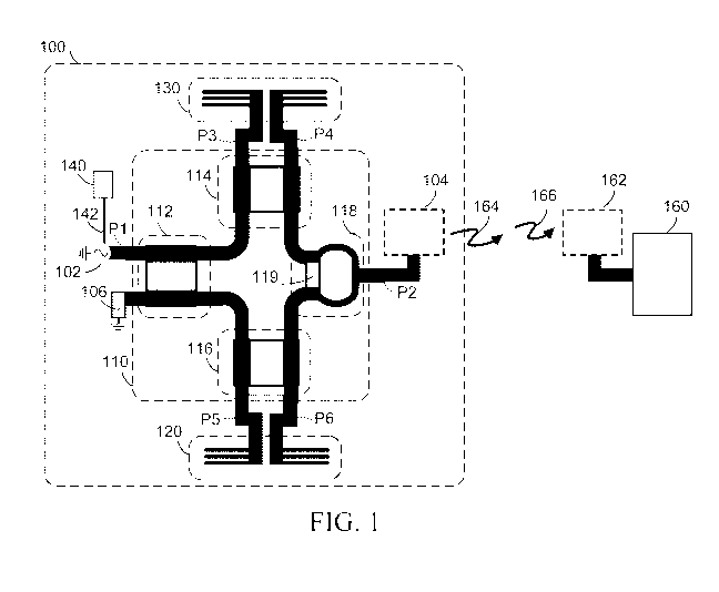
[0009] FIG. 1 is a schematic of a low-powered wireless sensor node and a
gateway node;
[0010] FIGS. 2(a), (b) and (c) are schematics of four-, five-, and six-port
modulator structures,
respectively, for use with a wireless sensor node;
[0011] FIG. 3 shows an example of a test sample and a reference sample in
relation to
.. corresponding sensing circuits of the wireless sensor node;
[0012] FIG. 4 is a schematic of a smart low-powered wireless/RFID sensor node
and a gateway
node;
[0013] FIG. 5 is a schematic of an unpowered wireless sensor node and a
gateway node;
[0014] FIG. 6 is a schematic of a smart unpowered wireless/RFD sensor node and
a gateway
.. node;
2
CA 03056467 2019-09-13
WO 2018/165755 PCT/CA2018/050306
[0015] FIG. 7 is a schematic of a single frequency unpowered wireless sensor
node and a
gateway node;
[0016] FIG. 8 is a schematic of a single/multiple frequency smart unpowered
wireless/RFID
sensor node;
[0017] FIGS. 9(a) and (b) are a photograph of a fabricated low-powered
wireless sensor and a
schematic of a portion of the fabricated low-powered wireless sensor,
respectively.
[0018] FIGS. 10(a) and (b) are a photograph of a fabricated pilot modulator
circuit and a
schematic of the fabricated pilot modulator circuit, respectively.
[0019] FIG. 11 is a photograph of a fabricated smart low-powered direct-
conversion sensor.
[0020] FIG. 12 is a photograph of a fabricated compact smart unpowered
wireless/RFID
sensor.
[0021] FIGS. 13(a) and (b) are graphs showing the measured amplitude and phase
of
transmission coefficient, respectively, of a fabricated pilot modulator in a
smart low-powered
direct-conversion sensor.
[0022] FIG. 14 is a graph depicting the relationship between measured phase
variations
compared to the free state of the experimental unpowered wireless/RFID sensor.
[0023] FIG. 15 is a graph showing calculated ErSUT and its error with respect
to actual values
for the experimental unpowered wireless/RFID sensor node.
[0024] FIGS. 16(a) and (b) are graphs showing the measured amplitude and phase
of
transmission coefficient, respectively, of a fabricated pilot modulator in a
smart unpowered
direct-conversion sensor.
[0025] FIGS. 17(a) and (b) are graphs plotting the constellation of
demodulated pilot and
sensor data, respectively, for the smart low-powered wireless/RFID sensor of
FIG. 11.
3
CA 03056467 2019-09-13
WO 2018/165755 PCT/CA2018/050306
[0026] FIGS. 18(a) and (b) are graphs plotting calculated Cr from the received
signals for
different samples for the smart low-powered wireless/RFD sensor of FIG. 11 and
the error of
calculated Cr with respect to the actual value, respectively.
DETAILED DESCRIPTION
[0027] The examples presented herein provide various embodiments of novel
wireless/RFID
sensors that integrate sensing and transmitting circuits. These sensors may be
employed in
near-to-zero (N-Zero) or zero power consumption applications, such as
industrial processes,
health care, water or food processing, and environmental/earth monitoring,
temperature,
sound, pressure, and so on.
[0028] In one aspect, an RFID/wireless sensor node includes a direct
conversion sensor with
multi-port structures, which simplifies the sensing system by integrating the
sensor and
modulator, thereby eliminating the need for a separate digitizer.
[0029] In another aspect, a low-powered wireless sensor comprises a signal
generator, a
modulator structure, two sensing circuits, and a transmitting element. For an
operating
frequency offo, a signal source at frequency of fo and a transmitting element
at fo connect to
input and output ports, respectively. The other ports connect to similar
sensors. One sensor
detects the physical, chemical, environmental, etc. variations or conditions
to be detected in
the sensor target (i.e. sensor data), while the other sensor provides
reference data. The detected
variations are used to modulate the input signal, which is transmitted to a
gateway node for
further analysis. The reference data can be used in a calibration procedure at
the receiver.
[0030] In another aspect, a smart low-powered wireless/RFID sensor comprises a
signal
generator, a modulator structure, a sensing circuit, a pilot sequence
generator, and a
transmitting element. For an operating frequency of fo , a signal source at
the frequency of fo
and a transmitting element atfo connect to input and output ports,
respectively. The other ports
operate as sensing and pilot ports, which connect to a sensor and a pilot
sequence generator,
respectively. The variations detected by the sensor provide the in-phase (or
quadrature) data.
The pilot sequence generator has two switches and four predefined loads. A
control signal
controls the switches to generate the pilot data, which provides the
quadrature (or in-phase)
4
CA 03056467 2019-09-13
WO 2018/165755 PCT/CA2018/050306
data. The in-phase and quadrature data is used to modulate the input signal,
which is
transmitted to a gateway node. The pilot data can be used for calibration and
channel estimation
to reduce the overall error at the receiver. The pilot data can be generated
based on a known
RFID, ZigBee , or Bluetooth standard by a microcontroller or transponder
integrated circuit
(IC) and used for item identification.
[0031] In another aspect, an unpowered wireless sensor comprises a receiving
element, a
frequency multiplier, a modulator structure, two sensing circuits, and a
transmitting element.
The receiving element absorbs a pure signal transmitted by a gateway node at
fi/M. The M-
times frequency multiplier comprises nonlinear elements and matching circuits,
changes the
frequency to fo and provides the signal to the input port of the modulator. A
transmitting
element atfi connects to the output port. The other ports connect to two
similar sensors. The
first sensor provides sensor data, while the other sensor provides reference
data. The detected
variations modulate the input signal, which is transmitted to a gateway node
for further
analysis. The reference data can be used in a calibration procedure at the
receiver.
[0032] In another aspect, a smart unpowered wireless/RFD sensor comprises a
receiving
element, a frequency multiplier, a modulator structure, a sensing circuit, a
low power pilot
sequence generator, and a transmitting element. The receiving element absorbs
a pure signal
transmitted by the gateway node at Jo/M. The M-times frequency multiplier
comprises
nonlinear elements, input and output matching circuits, and a DC-RE separator.
The DC part
of the frequency multiplier's output provides the power for the switches and
the pilot sequence
generator. The RE part of the frequency multiplier's output provides the input
signal of the
modulator at fi. A transmitting element atfi connects to the output port. The
other ports are
sensing and pilot ports, which connect to a sensor and a pilot sequence
generator, respectively.
The detected variations from the sensor provide the in-phase (or quadrature)
data. The pilot
sequence generator has two switches and predefined loads. A microcontroller or
a mid-
frequency signal (atfi), as pilot data, controls both switches. This provides
the quadrature (or
in-phase) data. The in-phase and quadrature data directly modulate the input
signal, which is
transmitted to a gateway node. The pilot data can be used for calibration and
channel estimation
to reduce the overall error at the receiver. Moreover, the pilot data can be
generated based on
5
CA 03056467 2019-09-13
WO 2018/165755 PCT/CA2018/050306
a known RFID, ZigBee, or Bluetooth standard by a microcontroller or
transponder IC, and
used in an identification process.
[0033] Still further, in another aspect a single frequency unpowered wireless
sensor comprises
a receiving element, a circulator, a modulator structure, two sensing
circuits, and a transmitting
element. The receiving element absorbs a pure signal transmitted by the
gateway node atfo and
the receive path of circulator provides the signal to the input port of the
modulator. A
transmitting element at fo connects to the output port. The other ports
connect to two similar
sensors. A first sensor provides sensor data, while the other sensor provides
reference data.
The detected variations (sensor data) modulate the input signal, which is
transmitted to a
gateway node for further analysis. The reference data can again be used in a
calibration
procedure at the receiver. At the gateway, a circulator separates the
transmitted pure signal
from the received modulated signal plus the self-coupled transmitted pure
signal. As the self-
coupled component is known to the gateway, it can be removed from the received
signal, which
can then be demodulated to extract the sensor data.
[0034] In yet another aspect, a single/multiple frequency smart unpowered
wireless/RFID
sensor comprises a receiving element, a circulator, a divider or diplexer, a
modulator structure,
a sensing circuit, a low power pilot sequence generator, and a transmitting
element. The
receiving element absorbs pure signals transmitted by the gateway node at fo
or various
frequencies offo andfi, and the receive path of circulator provides the
signals to the input port
of the modulator. In a single frequency system, the divider separates a part
of input signal at fo
to power up the node and provides the other part to the input port of the
modulator. In a double
frequency system, a diplexer separates absorbed frequencies and provides the
component with
frequencyfi to power up the node, and the component with frequency fo to the
input port of the
modulator. Using a RF to DC converter (rectifier), thefi signal provides power
for the switches
and pilot sequence generator. The fo signal is the input signal to the
modulator. A transmitting
element at fo connects to the output port. The other ports are sensing and
pilot ports, which
connect to a sensor and the pilot sequence generator, respectively. The
detected variations by
the sensor provide the in-phase (or quadrature) data. The pilot sequence
generator has two
switches and predefined loads. A microcontroller or a mid-frequency signal (at
fm) as the pilot
6
CA 03056467 2019-09-13
WO 2018/165755 PCT/CA2018/050306
data controls both switches. The pilot data provides the quadrature (or in-
phase) data. The in-
phase and quadrature data directly modulate the input signal and transmits to
a gateway node.
The pilot data can be used in calibration and channel estimation to reduce the
overall error at
the receiver. Again, the pilot data can be generated based on a known RFID,
ZigBee, or
Bluetooth standard with a microcontroller or transponder IC, and can also be
used in an
identification (such as an RFID) process. At the gateway, a circulator
separates the transmitted
pure signal from the received modulated signal plus the self-coupled
transmitted pure signal.
As the self-coupled part is known to the gateway, it can be removed from the
received signal,
which is then demodulated to extract the sensed data.
[0035] FIGS. 1 through 8 illustrate the structure of different embodiments of
a low-powered
or unpowered wireless/RFD sensor in accordance with the aspects mentioned
above.
Low-Powered Wireless Sensor
[0036] Referring first to FIG. 1, a first embodiment of a low-powered wireless
sensor 100 is
shown, comprising a signal generator 102, a modulator 110, first and second
sensing circuits
120, 130, and a transmitting element 104. In this example, the signal
generator 102 is a low-
powered crystal oscillator and the transmitting element 104 is an antenna. A
power source 140
provides power to the signal generator 102 via a connection 142. Although
shown as a battery
in this case, the power source 140 may be any suitable type of power source,
such as a solar
cell, a piezoelectric material, a super-capacitor, or a power-harvesting
system.
[0037] The modulator 110 may be any type of circuit adapted to modulate a
signal onto another
signal, such as a planar multi-port direct conversion structure. Multi-port
structures having
more than four ports can collect different phase-shifted versions of the input
signal; in this
example, the modulator 110 is a direct conversion six-port modulator
consisting of three hybrid
90 couplers 112, 114, and 116 and one in-phase power combiner 118. However, a
four-, five-
, or six-port modulator structure (as shown in FIG. 2) may be employed with
two (P3 and P4),
three (P3, P4 and P5), and four (P3, P4, P5, and P6) sensing ports,
respectively. A 100-ohm
isolation resistor 119 is provided for the power combiner and a 50-ohm
matching resistor 106
is used to terminate the unneeded port. The signal generator 102 at operating
frequency fo
7
CA 03056467 2019-09-13
WO 2018/165755 PCT/CA2018/050306
connects to the input port P1, and the transmitting element 104, configured to
operate at fo,
connects to the output port P2. The first pair of sensor ports P5, P6 connect
to the first sensing
circuit 120 and the second pair of sensor ports P3 and P4 connect to the
second sensing circuit
130.
[0038] The sensing circuits 120, 130 in this example are both microwave
resonator sensors.
However, any type of sensitive circuit that can provide variable input
impedance in response
to a detected sample ("sensor data") may be used instead of the illustrated
resonator sensors in
this implementation, and is contemplated herein. One of the first and second
sensing circuits
120, 130 detects the variations or conditions to be monitored by the low-power
wireless sensor;
the other sensing circuit 130 or 120 operates as a reference, generating
reference data. The data
from the first and second sensing circuits 120, 130 are each used by the
couplers 116, 114 to
modify the input signal fo received at the port P1. The modified signals are
combined at the
combiner 118 and output as a modulated output signal at port P2, as discussed
in further detail
below. The modulated output signal is then transmitted by the transmitting
element 104 as
transmitted signal 164 and received by a receiving element 162 (e.g., an
antenna) as received
signal 166 at a node 160. The transmitting element 104 and the receiving
element 162 may be
any suitable transmitting and receiving element configured for communication
using a wireless
(i.e., not fixed) connection, such as by electromagnetic, inductive,
capacitive, and optical
coupling or transmission. The node 160 may be a gateway node connected to
other elements
in a network or system, and may be configured to extract the sensor data from
the received
signal 166 for analysis, and to process data. Thus, the node 160 may include a
microcontroller,
and may be any suitable computing device provided with or in communication
with a suitable
receiving element 162. The reference data encoded in the received signal 166
can be used by
the node 160 for calibrating the first sensing circuit 120.
[0039] In one illustrative application shown in FIG. 3, the low-powered
wireless sensor node
100 of FIG. 1 is used as a material detector. A reference sample (Ref) 222 and
a sample under
test (SUT) 232 are placed on resonator sensing circuits 220 and 230,
respectively. The sensing
circuit 230 detects the condition of the test sample 232 and generates sensor
data, which
directly modulates the input signal of frequency fo to generate a modulated
output signal. The
8
CA 03056467 2019-09-13
WO 2018/165755 PCT/CA2018/050306
transmitting element 104 transmits the modulated output signal as the
transmitted signal 164
having frequency fo to the node 160 via the receiving element 162 for further
analysis.
[0040] Referring again to FIG. 1, the signal from the low-powered oscillator
102 is divided
into in-phase (I) and quadrature (Q) paths by the first coupler 112. For a
given reference input
signal aw (t) at input port Pi, the output signal aT (t) at output port Pj in
a six-port circuit as in
FIG. 1 can be represented as:
6
aT11S21FaLO
1=3
fsil =se' (1)
1S2, =IS 2,leA
where Su are scattering parameters between ports Pi and Pj and Fi is the
reflection coefficient.
In order to have a good reflection coefficient at the input port, the
following equation should
be satisfied:
6
0. (2)
1=3
[0041] A simple way to implement the above condition is using the quadrature
reflection phase
shifting characteristics of the couplers 114 and 116. In these structures,
reflections from ports
P3-P4 and P5-P6 cancel each other out when the reflectors at P3 and P5 are the
same as P4 and
P6, respectively. In that case, the sensing circuits 220 and 230 in FIG. 1
produce variable loads
for the sample under test (SUT) 232 and reference sample (Ref) 222,
respectively, complex
reflection coefficients of F SUT = ISUT jQSUT and FRef= IRef+ jQRef, from P3
to P4 and from P5
to P6, respectively. Furthermore, in the case of an ideal combiner 118 and
couplers 112-114,
the transmitted signal at P2 is simplified as:
(F Ref if SUT)
aT = ____________________________ aLO (3)
2
and the overall transmission coefficient from P1 to P2 is:
9
CA 03056467 2019-09-13
WO 2018/165755 PCT/CA2018/050306
T = (F Ref jF suT) I 2 (4)
[0042] Therefore, the output signal is composed of two vector components, i.e.
FRef and jFsuT
which are in a semi-orthogonal vector space and easy to separate at the
receiver.
[0043] On the receiving end at the node 160, a quadrature demodulator may
separate the real
and imaginary parts of the received signal as:
FR = IR jQR, (5)
[0044] In the ideal communication channel, the normalized transmitted signal
164 is equal to
the received one 166 and considering the (4), we have:
FR = T = (F ReT J' SUT) I 2, (6)
[0045] At the first step, when the system is started in the free state (RO)
for both the reference
sample (Ref) 222 and the sample under test (SUT) 232, the F Ref is equal to
the jFsuT and can
be calculated simply from FRO by:
'Ref = FRO ¨ jfRO, (7)
[0046] Then, for each sample under test (SUT) 232 we have:
FSUT (F Ref 2FR ), (8)
and from the calculated F SUT and from F versus the relative permittivity Cr
of the sensor, the
value of the relative permittivity Cr of the sample under test 232 can be
estimated.
Smart Low-Powered Wireless/RFID Sensor
[0047] FIG. 4 illustrates a further embodiment of a low-powered sensor, here a
smart low-
powered wireless/RFD sensor 300. The embodiments described herein referred to
as "smart"
are embodiments incorporating pilot data and identification data, as described
below. It will be
appreciated by those skilled in the art that the example "smart" sensors
described here can
include further capabilities¨for example, additional sensing
structures¨generating additional
CA 03056467 2019-09-13
WO 2018/165755 PCT/CA2018/050306
data that may be encoded in the signals transmitted from the sensor 300. The
sensor 300
comprises a signal generator 102, a modulator 110, a sensing circuit 120, a
pilot sequence
generator 330, and a transmitting element 104. The signal generator 102,
modulator 110,
sensing circuit 120, and transmitting element 104 may be the same types as
described above.
[0048] The signal generator 102, operating at frequency fo, connects to the
input port P1 of the
modulator 110 and the transmitting element 104, also operating at frequencyfo,
connects to the
output port P2. The sensing circuit 120 is connected to the sensor ports P5
and P6, while pilot
sequence generator 330 is connected to the pilot ports P3 and P4. The
modulator 110 produces
a directly modulated output signal at port P2 using sensor data generated by
the first sensing
.. circuit 120 and pilot data generated by the pilot sequence generator 330.
The pilot data may be
known to the node 160. In the examples herein, the pilot data may comprise a
fixed value such
as an identifier (e.g., such as that used in for RFID identification), or
optionally other arbitrary
or non-arbitrary data sequences comprising with ZigBee, Bluetooth, or other
standards. The
pilot data, when obtained by the node 160, may be used in processing the
sensor data also
received by the node 160.
[0049] The pilot sequence generator 330 has two N-state (multi-state) switches
332 and 334
(thus, N = 2 in this example), each connecting to one of a corresponding set
of N predefined
loads 340, 350 respectively. In the example of FIG. 4, there are thus four
predefined loads 342
(short circuit), 344 (open circuit), 352 (short circuit), and 354 (open
circuit). A control signal
338 from the controller 336, preferably a mid-frequency signal, provides the
in-phase pilot
data /(t) to control the multi-state switches 332 and 334 at ports P3 and P4
in the upper branch
of the modulator 110. For simplicity, only two marginal reflection states
provided by the
predefined loads are available for selection: short (loads 342, 352) and open
(loads 344, 354)
circuits. This fixes the complex reflection coefficients of Fo and -Fo for
/(t) = 0 and 1,
respectively. In other implementations, the loads 342, 344, 352, 354 may be
provided by
variable load devices such as resistors or capacitors with voltage- or current-
controlled
impedances.
11
CA 03056467 2019-09-13
WO 2018/165755 PCT/CA2018/050306
[0050] In the bottom branch of the modulator 110, the ports P5 and P5 are
connected to the
sensing circuit 120, which provides a variable load with a complex reflection
coefficient of
FSUT. Any change in the input impedance of sensing circuit 120, due to the
variations or
conditions of a sample under test (SUT) 232 placed on the sensing circuit 120,
is directly
modulated in the output signal at P6. The combiner 118 is used to combine the
signals of the
upper and lower branches of the modulator 110. In the case of ideal combiners
118 and
couplers 112-116, the output signal at port P2 can be simplified as:
aõ =2S31S23((-1)1(t)F 0+ jf suT)aL0 ,1 = 0,1. (9)
[0051] The output signal is thus composed of two vector components, i.e. (-
1)40F0 and jfsuT,
.. with the first one being known at the node 160. The output signal is
transmitted using
transmitting element 104 and is sent as transmitted signal 164 with
frequencyfo. The signal is
received as received signal 166 by receiving element 162 of the node 160,
where the received
signal 166 can be decoded and analyzed. The pilot data extracted from the
received signal 166
may be used for identification (such as an RFID), sensor calibration, and
channel estimation
purposes at the node 160.
[0052] The controller 336 in these examples can be a microcontroller adapted
to implement
any suitable signal type that can be used to provide pilot data, including
standard signals, such
as ZigBee, Bluetooth, and RFID. Thus, the sensor 300 can function both as an
RFID tag or
similar wireless identification tag, and as a sensor device in a wireless
sensor network.
Alternatively, the controller 336 may operate as a mid-frequency signal
generator operating at
frequency fi to generate a simple, unique data sequence while consuming less
power than a
controller generating standard signals.
[0053] A power source 320 provides power to the signal generator 102 via a
connection 322,
to the controller 336 via another connection 324, and to the switches 332 and
334 via a further
connection 326. Although shown as a battery in this case, as explained above
the power source
12
CA 03056467 2019-09-13
WO 2018/165755 PCT/CA2018/050306
320 may be any suitable type of power source, such as a solar cell, a
piezoelectric material, a
super-capacitor, or a power-harvesting system.
Unpowered Wireless Sensor
[0054] In another embodiment, an unpowered wireless sensor 400 is provided, as
shown in
FIG. 5. The sensor 400 comprises a receiving element 402, a frequency
multiplier 410, a
modulator 110, first and second sensing circuits 120, 130, and a transmitting
element 104. The
modulator 110, sensing circuits 120 and 130, and the transmitting element 104
may be the
same types as described above. The unpowered wireless sensor 400 operates in
conjunction
with a node 460, which as before may be a gateway node. The node 460 is
provided with a
receiving element 462 as well as a transmitting element 472. The receiving and
transmitting
elements 462, 472 may be antennas as in the illustrated example.
[0055] The node 460 transmits, via its transmitting element 472, a pure signal
474 of frequency
of fo/M which is received by the sensor 400 by its receiving element 402 as
received signal
476. An M-times frequency multiplier 410, in this example a passive diode
doubler (i.e., M=2),
comprises nonlinear elements 412, such as diodes or transistors, and input and
output matching
circuits 414 and 416. The due to its nonlinearity, the output signal of the
diode 412 has a
harmonic at M times the frequency input (in this example, at 2x the input).
Consequently, the
output matching circuit 416 only passes the signal with frequency fo. This
modified signal is
provided as input at port P1 of the modulator 110.
[0056] The ports P3 and P4 of the modulator 110 connect to the first sensing
circuit 120, while
the ports P5 and P6 connect to the second sensing circuit 130. As in the first
embodiment
described above, one of the first and second sensing circuits 120, 130 detects
the variations or
conditions to be monitored by the low-power wireless sensor, producing sensor
data; the other
sensing circuit 130 or 120 operates as a reference, generating reference data.
If the unpowered
wireless sensor 400 is implemented as a material detector, a reference sample
222 and a test
sample 232 are placed on the first and second sensing circuits 120 and 130, as
described above
with reference to FIG. 3. The sensor data from the first and second sensing
circuits 120, 130
are used by the couplers to modulate the input signal at frequency fo received
from the input
13
CA 03056467 2019-09-13
WO 2018/165755 PCT/CA2018/050306
port P1. The modulated signal is output at port P2 to the transmitting element
104, which
operates at frequencyfo to transmit the modified output signal as output
signal 464 to the node
460. The architecture of the unpowered sensor 400 is thus similar to the low-
powered sensor,
except that the input signal at port P1 is extracted from the received signal
474, and there is no
power source in the sensor 400.
[0057] The receiving element 462 of the node 460 receives the signal from the
sensor 400 as
received signal 466. On receipt of the signal 466, the node 160 may extract
the sensor data for
analysis, while the reference data may be extracted for use in calibration.
The frequency fo of
the received wave 466 is in a different region of the frequency domain from
the originally
transmitted signal 474 at frequency folM.
[0058] The corresponding pairs of transmitting elements and receiving elements
104, 462 and
462, 472 may be antennas or any other suitable transmitting and receiving
element, as
mentioned above.
Smart Unpowered Wireless/RFD Sensor
[0059] FIG. 6 illustrates a smart unpowered wireless/RFID sensor 500
embodiment. The
architecture is similar to the smart low-powered sensor examples above, except
that the input
signal and bias signals powering the sensor 500 are obtained from a received
signal. The sensor
500 comprises a receiving element 402, a frequency multiplier 510, a modulator
110, a sensing
circuit 120, a pilot sequence generator 330, and a transmitting element 104.
These components
may be the same type as the components described above with reference to the
other illustrated
embodiments. The node 460 may be configured in a similar manner to the node
460 described
above with reference to FIG. 5, and receiving and transmitting elements 472,
402 and 104, 462
may be any suitable elements as discussed above.
[0060] In this embodiment, the node 460 transmits via its transmitting element
472 a pure
signal 476 with a frequency offo/M. The pure signal is received as received
signal 476 by the
receiving element 402 of the sensor 500 and passed to an M-times frequency
multiplier 510.
The M-times frequency multiplier 510 (M=2 in this example) comprises nonlinear
elements
14
CA 03056467 2019-09-13
WO 2018/165755 PCT/CA2018/050306
512 and input/output matching circuits 514/516. Then, a low-pass filter inside
the DC-RF
separator 518 extracts the DC component of the signal. This portion of the
signal is used as the
bias for the controller 336 and switches 332, 334 of the pilot sequence
generator 330 via lines
520, 522 and 524. The RF component having afi harmonic is extracted using a
band pass filter
of the separator 518, and is input to the port P1 of the modulator 110. The
input signal to the
modulator 110 at port P1 therefore has frequency fi.
[0061] Ports P3, P4 are connected to a pilot sequence generator 330 and ports
P5, P6 are
connected to a sensing circuit 120. The pilot sequence generator 330 and
sensing circuit 120
may be configured as described above with reference to FIG. 4. As in the
example of FIG. 4,
the pilot data generated by the pilot sequence generator 330 and the sensor
data from the
sensing circuit 120 provide the quadrature and in-phase data (or vice versa)
used by the
modulator 110 to directly modulate the signal output at port P2, which has
frequency Jo. Also
as described above with respect to FIG. 4, the signal 464 transmitted by the
transmitting
element 104 connected to port P2 is received as received signal 466 by
receiving element 462
of the node 460, where the received signal 466 can be decoded and analyzed.
The pilot data
extracted from the received signal 466 may be used for identification (such as
an RFID), sensor
calibration, and channel estimation purposes at the node 460.
Single-Frequency Unpowered Wireless Sensor
[0062] FIG. 7 illustrates a further embodiment, a single-frequency unpowered
wireless sensor
600. The sensor 600 comprises a receiving/transmitting element 603, a
receive/transmit
separator 602, a modulator 110, and two sensing circuits 120, 130. The
modulator 110 and
sensing circuits 120, 130 may be components as generally described above with
reference to
other embodiments. The separator 602 may be a circulator.
[0063] The node 660, which as before may be a gateway node, is provided with a
receiver 662
(which in this example includes a down-converter and processor) and a signal
generator 664
in communication with a circulator 666. The signal generator 664 generates a
pure signal at
frequency fo, which is transmitted via the circulator 666 to the
receiving/transmitting element
CA 03056467 2019-09-13
WO 2018/165755 PCT/CA2018/050306
668 and thence as signal 674 to the sensor 600. The receiving/transmitting
elements 104, 668
may be an antenna or any other suitable component as discussed above.
[0064] The receiving element 603 receives the signal generated by the node 660
as received
signal 676. This signal is received by a first port of the separator 602,
which passes the received
signal through a second port to the input port P1 of the modulator 110. The
output port P2 of
the modulator 110 is connected to a third port of the separator 602. The other
ports P3, P4, P5,
and P6 of the modulator 110 are connected to two similar sensing circuits 120,
130, generally
as described above with reference to FIGS. 1 and 5. Thus, one sensing circuit
120, 130 detects
variations or conditions in the target to produce sensor data, while the other
sensing circuit
.. 130, 120 operates as a reference, producing reference data. The sensor 600
can be used as a
material detector in the same general manner as described above with reference
to FIG. 3.
[0065] The sensor data and reference data produced by the sensing circuits
120, 130 directly
modulate the input signal in the modulator 110. The modulated signal is output
to port P2, and
transmitted by the receiving/transmitting element 603 as output signal 604.
This signal is
received by the receiving/transmitting element 668 of the gateway 660, then
passed via the
circulator 666 to the receiver 662. In a self calibration process, the self-
coupling of signal 664
into the receiver 662 is determined. Then, the node 660 can remove the self-
coupled signal 667
from the received signal, and extract the sensor data for analysis. The
reference data may also
be extracted by the node 660, and used for calibration.
Single/Multiple-Frequency Smart Unpowered Wireless/RFD Sensor
[0066] In a further embodiment, a single/multiple frequency smart unpowered
wireless/RFID
sensor 700 is provided, as illustrated in FIG. 8. The sensor 700 in this
embodiment comprises
a receiving/transmitting element 603, a receive/transmit separator 602, a
modulator 110, a
sensing circuit 120, and a pilot sequence generator 330. These components are
generally
described above with reference to other embodiments.
[0067] The node 660 is provided with a receiver 662 and a signal generator 664
in
communication with a circulator 666. The signal generator 664 generates a pure
signal at
16
CA 03056467 2019-09-13
WO 2018/165755 PCT/CA2018/050306
frequencyfi, or at various frequenciesfi andfi. The signal is transmitted via
the circulator 666
to the receiving/transmitting element 668 and thence as signal 674 to the
sensor 600. The
receiving/transmitting elements 104, 668 may be an antenna or any other
suitable component
as discussed above.
[0068] The receiving/transmitting element 603 of the sensor 700 receives the
signal generated
by the node 660 as received signal 676. The received signal 676 is provided to
a first port of
the separator 602, which passes the received signal through a second port to a
divider or
diplexer 718. In a single frequency system where the input signal at the
separator 602 is at a
single frequency fi, the divider 718 directs part of the input signal to an RF
to DC converter
710, and the remainder of the signal to the input port P1 of the modulator
110. The RF to DC
converter 710 comprises nonlinear elements (such as diodes or transistors) 712
and input and
output matching circuits 714, 716 to produce an output DC signal, which
provides power for
the pilot sequence generator 330 via lines 522 (to the controller 336) and the
switches 332 and
334 (via line 524). In a mixed frequency system, a diplexer 718 diverts the
portion of the signal
with frequency fi to the RF to DC converter 710 to power the pilot sequence
generator 330,
and the frequencyfi portion to the input port P1 of the modulator 110.
[0069] The output port P2 of the modulator 110 is connected to a third port of
the separator
602, while ports P5 and P6 are connected to the sensing circuit 120, and ports
P3 and P4 are
connected to the pilot sequence generator 330. As described above, the pilot
sequence
generator 330 operates to produce pilot data input to the modulator 110, while
the sensing
circuit 120 produces sensor data input to the modulator 110. These inputs to
the modulator 110
provide the quadrature and in-phase parts (or vice versa) that are used to
directly modulate the
input signal received at port P1. The modulated output signal is output at P2
to the connected
receiving/transmitting element 603, which transmits the modulated output
signal as signal 604
to the node 660.
[0070] The receiving/transmitting element 668 of the node 660 receives the
signal as received
signal 606, and passes the received signal to the receiver 662 via the
circulator 666. As
mentioned above, the self-coupled portion of the signal 667 can be removed
from the received
17
CA 03056467 2019-09-13
WO 2018/165755 PCT/CA2018/050306
signal at the receiver 662, and the sensor and pilot data can be extracted for
analysis,
calibration, and channel estimation.
Experimental Results
[0071] Each sensor subsystem described above was designed, fabricated, and
tested at an
operating frequency of 2.45 GHz. The test system employed a R&S ZVA67 vector
network
analyzer (VNA) and a TektronixTm DP071604C digital oscilloscope for scattering
parameter
and time domain signal measurements, respectively. Simple patch antennas were
used for
wireless transmission to and from the sensor. Signals received from the
sensors were collected
by the oscilloscope and processed to extract the sensing information and pilot
data.
[0072] The overall system was then tested with various standard samples. All
circuits are
fabricated with printed circuit technology using R04003 laminate from Rogers
Corporation,
Arizona, USA, which has a relative permittivity of about 3.55, thickness of
0.508 mm, and a
loss tangent of 0.0027.
[0073] FIG. 9(a) is a photograph of the fabricated low-powered sensor
represented
schematically in FIG. 1, with dimensions indicated in FIG. 9(b) as set out in
Table 1:
Parameter Quantity (mm) Parameter Quantity (mm)
wo 1.13 Lo 5.00
wi 1.13 Li 18.8
W2 1.91 L2 18.8
W3 1.13 L3 22.4
W4 0.30 L4 10.2
W5 1.13 L5 5.00
18
CA 03056467 2019-09-13
WO 2018/165755 PCT/CA2018/050306
W6 0.25 L6 2.35
S4 0.7
Table 1. Dimensions of fabricated low-powered sensor.
[0074] The sensing circuit in this example consists of a quadrature coupler
and a sample area
which provides a SUT-related capacitive loading for the coupler. Coupons were
extracted from
various Rogers Corporation lamintes by removing the metal foil, thus yielding
samples with Cr
= 2.2, 3.55, 4.5, 6.0 ,10.2, and 12.85. Each of these samples were placed on
the sample area.
[0075] FIGS. 10(a) and (b) are a photograph and schematic, respectively, of a
fabricated pilot
modulator circuit with the same dimensions indicated in Table 1. The pilot
modulator circuit
is composed of a quadrature coupler and two low insertion-loss Infineon
Technologies
BGS12SN6 RE MOS switches SW1 and 5W2. The bias voltage Vmas was 3.4V and the
control
voltage Vca representing pilot data was modified by a periodic pulse between
OV and 3V. The
time between control and RF is about 500ns for this type of switch;
accordingly, the frequency
of the pilot modulator circuit 900 was selected as 100 KHz to ensure
sufficient time for stable
switching between two states in each period. However, in principle there is no
frequency
limitation if a correspondingly faster switch is used.
[0076] FIG. 11 is a photograph of a fabricated smart low-powered direct-
conversion sensor,
using the same dimensions as in FIG. 9, and in which one sensing circuit has
been replaced by
the pilot modulator circuit of FIGS. 10(a) and (b).
[0077] A compact smart unpowered direct-conversion sensor was also fabricated,
as shown in
FIG. 12, to demonstrate the application of the inventive concepts herein to
miniature sensor
nodes. The six-port structure was used. It can be seen that that by using a
low-profile sub-
miniature power dividers PD (PD2328J505052HF from AnarenTM) and hybrid 90
couplers
H90 (C2327J5003AHF from AnarenTm), the footprint of the sensor structure can
be
significantly reduced. The selected switches (InfineonTM BGS12SN6) and mid-
frequency
signal generator (AbraconTM ASTMTXK 32.768KHZ) are also very small. The
oscillator used
19
CA 03056467 2019-09-13
WO 2018/165755 PCT/CA2018/050306
in this example (AbraconTM TCXO 32.768KHz) is high performance with ultra-low
current
consumption.
[0078] FIGS. 13(a) and (b) shows the measured (a) magnitude and (b) phase of
the
transmission coefficient (FT) between ports P2 and P1 of the fabricated smart
low-powered
direct-conversion sensor, using the six samples mentioned above. As expected
for this
symmetric structure and its capacitive loads, the magnitude of FT in FIG.
13(a) is
approximately constant and close to 1.
[0079] The variations of phase of F SUT with respect to the free state of
sensor F Ref (i.e. Cr = 1)
is approximately a linear function of Cr, as can be seen in FIG. 14. This
curve can be used at
the receiver to find the Cr value of SUT from demodulated transmission
coefficient and as they
are linearly dependent, the calibration procedure is simple.
[0080] FIG. 15 shows the calculated CrSUT and its error with respect to the
actual value for the
fabricated unpowered direct-conversion sensor. In these calculations, the
calculated F SUT was
normalized by F Ref and then mapped into the curve shown in FIG. 14 to find
Cr. As can be seen
in FIG. 15, was less than 16%. It should be noted that this error is a
function of the transmission
channel and may be degraded in a noisy environment.
[0081] FIGS. 16(a) and (b) show the measured (a) amplitude and (b) phase of
transmission
coefficient, respectively, of the fabricated pilot modulator in the fabricated
smart unpowered
direct-conversion sensor. The amplitude of FT in FIG. 16(a) is approximately
constant and
close to 1, and the phase difference between two states in FIG. 16(b) is 180 ,
which reflected
design expectations.
[0082] FIGS. 17(a) and (b) show the constellation (imaginary versus real
component of a
signal) of the demodulated (a) pilot and (b) sensor data, respectively, for
the smart direct-
conversion sensor. The constellation of the pilot data was approximately
constant while the
sensor data varied in proportion to Cr.
[0083] FIGS. 18(a) and (b) show (a) the calculated Cr from the received
signals for different
samples in a calibration process and (b) the error of calculated Cr with
respect to the actual
CA 03056467 2019-09-13
WO 2018/165755 PCT/CA2018/050306
value for the smart direct-conversion sensor, respectively. In these
calculations, the free state
and one sample, as indicated in the legends, were used in a linear
approximation. Based on the
result for the given sample, the other five Cr values were calculated based on
the extracted
QsuT/IsuT and the above linear approximation. As can be seen in FIG. 18(b),
the error related
to the Cr of the calibration sample. However, based on the desired range of
Cr, a sample can be
used as the standard sample to minimize error. In the presented range of Cr,
the error of
estimation was kept below 15%. It should be noted that this error is a
function of the
transmission channel and may be degraded in an industrial or other noisy
environment.
[0084] It will be appreciated by those skilled in the art that the foregoing
embodiments
demonstrate a wireless sensor using a modulator, such as a multi-port direct
conversion
structure, in combination with at least one sensing circuit and either
reference or pilot data to
modify an input signal to the modulator. The resultant modulated output signal
can then be
transmitted via an antenna or other suitable means to a receiving unit, such
as the
aforementioned nodes, which can extract the sensor data from the sensing
circuit and the
reference/pilot data for analysis and processing. Optionally, the wireless
sensor can be powered
with an on-board power source; but alternatively, the sensor may obtain or
harvest power from
another source, or be powered by the signal transmitted by the receiving unit.
The receiving
unit may be a card reader, smart phone, or other device adapted for
communication with the
wireless sensor. The wireless sensor, in some embodiments, can thus function
as a combined
sensor node and RFID tag, and may furthermore operate at a variety of
frequencies
encompassing radio, telecommunications, and ISM bands. The wireless sensor may
furthermore communicate in a wideband or ultra-wideband mode, or in multiple
bands, to
reduce power consumption or environmental noise. Some or all of the components
of the
wireless sensor may be provided in compact form, or as integrated circuits.
[0085] The present invention has been described above and shown in the
drawings by way of
example embodiments and applications, having regard to the accompanying
drawings. These
are merely illustrative of the present invention; it is not necessary for a
particular feature of a
particular embodiment to be used exclusively with that particular embodiment.
Instead, any of
the features described above and/or depicted in the drawings can be combined
with any of the
21
CA 03056467 2019-09-13
WO 2018/165755 PCT/CA2018/050306
example embodiments, in addition to or in substitution for any of the other
features of those
example embodiments. One embodiment's features are not mutually exclusive to
another
exemplary embodiment's features. Further, it is not necessary for all features
of an example
embodiment to be used. Instead, any of the features described above can be
used, without any
other particular feature or features also being used. Accordingly, various
changes and
modifications can be made to the example embodiments and uses without
departing from the
scope of the invention as described herein.
22