Note: Descriptions are shown in the official language in which they were submitted.
CA 03056519 2019-09-13
WO 2018/185032 PCT/EP2018/058325
1
Implantable Optical Sensor With Hermetically Sealed Cover Cap
Field of the invention
The present invention relates to an optical assembly, e.g. an implantable
optical sensor,
comprising a substrate and an optical microstructure integrated with the
substrate, the optical
microstructure being positioned to form an optical interaction area on a part
of a surface of the
substrate. In a further aspect, the present invention relates to a method of
manufacturing an
optical assembly, the method comprising providing a substrate with an
integrated optical
microstructure forming an optical interaction area.
Background art
International Patent publication W02016/137444 discloses a sensor and a method
for
measuring an analyte in a medium within a living animal. The sensor includes
an inductive
element, a charge storage device and a memory. The sensor performs analyte
measurements
initiated by an external device using power received from the external device
and conveys analyte
measurements to the external device using the inductive element. The sensor is
entirely sealed
in a glass capsule
US patent publication US 6,981,806 B2 discloses a method for micro-hermetic
packaging
an optical device. The method comprises forming a micro-hermetic cavity on a
substrate,
providing a transmission optical waveguide on the substrate and sealing an
optical device within
the micro-hermetic cavity. A lid separate from the first substrate is employed
for the sealing
process or the micro-hermetic cavity is provided on the lid and sealed on to
the first surface. The
optical device may be positioned within the cavity for optical power transfer
with the optical
waveguide.
US 2004/0245425 Al discloses a hybrid electro-optical device which has a
portion
defining a mounting location for optoelectronic components such as laser
sources, photodetector
diodes, LEDs, requiring local hermetic protection of the bare chips. A planar
lightwave circuit
(PLC) waveguide structure formed on the substrate extends to the mounting
location to define an
optical signal feed-through for the device. At least one electrode is
associated with the planar
lightwave circuit waveguide structure and extends said mounting location to
define an electrical
signal feed-through for the device. A ring-like structure continuously
surrounds said mounting
location and a continuous cover member is soldered thereon to cover and
hermetically seal the
mounting location. As a result of this ring-like structure, which is a metal
rim, the device is not
suitable for wafer scale production.
A well-known approach in art used to protect optical assemblies is by using
e.g. a titanium
box. However this approach has the drawbacks of not being a wafer scale
process and each
device needs to be processed separately, thereby making the approach costly.
If an optical
CA 03056519 2019-09-13
WO 2018/185032 PCT/EP2018/058325
2
measurement needs to be carried out in an optical assembly, a feedthrough
needs to be foreseen;
which is not standard. A further approach is using parylene-c coating, but
then it is not possible
to test a device for a successful hermetic packaging. Another approach used,
e.g. in
telecommunications, and data communications applications, is by using a wafer
scale capping in
which the feedthroughs are made through the wafer scale cap. These
feedthroughs are weak
points especially when regarded in relation to a desired long life time.
Summary of the invention
The present invention seeks to provide an optical assembly, e.g. an
implantable optical
sensor, which is particularly suited to interact optically with harsh
environments. More in particular,
the present invention seeks to provide an optical assembly having an optical
interaction area to
provide exposure to a fluid, such as body fluids, as well as associated
further active components
which are sealed from the fluid, in order to have a reliable and safely
working optical assembly.
Further, the present invention seeks to provide an optical assembly which can
be produced by
wafer scale processes.
According to the present invention, an optical assembly as defined above is
provided,
further comprising a cover cap on a part of the substrate adjacent to the
optical interaction area.
At least one active component is positioned in a sealed cavity which is formed
between the
surface and the cover cap. The substrate comprises at least one optical
feedthrough extending
from the sealed cavity to the optical interaction area. As a result, there is
no need to protrude the
cover cap for reasons of communicating or interfacing with electronic
components within the
sealed cavity. This effectively shields the electronic component, and more
specifically the
electrical components of the optical assembly from contact with the fluid
during use, without
influencing the optical properties and measurement capabilities of the optical
assembly.
Furthermore, optical communication is possible from the active component(s) in
the sealed cavity
to an optical microstructure (which is present on the substrate) and back.
The cover cap is hermetically sealed to said substrate part by wafer-to-wafer
bonding
technology or another wafer-level hermetic packaging technique. The resulting
device may be
characterized by absence of any metal rim or ring-like structure as described
in US 2004/0245425
Al to prepare the substrate for sealing the cover cap thereto, absence of
soldering material
between the cover cap and the substrate, i.e. the bottom edge of the cap may
be in direct contact
with the surface of the substrate. Furthermore, the resulting device may be
characterized by
absence of a flange at the bottom edge of the cover cap, i.e. the techniques
used for sealing the
cap onto the substrate do not require such a flange.
A further aspect the present invention relates to a method of manufacturing an
optical
assembly as defined above, wherein the method further comprises providing at
least one active
component on the surface adjacent to the optical interaction area, and
providing a cover cap on
a part of the substrate to form a sealed cavity where the at least one active
component is
CA 03056519 2019-09-13
WO 2018/185032 PCT/EP2018/058325
3
positioned. Furthermore, the method comprises sealing the cover cap to the
substrate by wafer-
to-wafer bonding technology or another wafer-level hermetic packaging
technique, and providing
at least one optical feedthrough extending from the sealed cavity to the
optical interaction area
(i.e. without protruding the cap). As the method uses techniques which are
compatible with the
manufacturing steps for other elements of the optical assembly, the method can
be implemented
as an efficient and cost-effective manufacturing method.
Short description of drawings
The present invention will be discussed in more detail below, with reference
to the
attached drawings, in which,
Fig. 1 shows a schematic cross sectional view of an optical assembly according
to a first
embodiment of the present invention;
Fig. 2 shows a schematic cross sectional view of an optical assembly according
to a
second embodiment of the present invention;
Fig. 3 shows a schematic cross sectional view of an optical assembly according
to a
further embodiment of the present invention;
Fig. 4 shows a schematic top view of an optical assembly according to an even
further
embodiment of the present invention; and
Fig. 5 shows a schematic cross sectional view of an optical assembly according
to an
even further embodiment of the present invention.
Description of embodiments
Optical assemblies which have an intended use as implantable (or (partially)
immersed)
optical sensors mostly have bulky components in the form of electronic and/or
optoelectronic
components. These may comprise electronic circuitry requiring an electrical
power supply for its
operation, and this circuitry must be completely sealed and protected from any
moisture. When
circuitry is exposed to an environment of the optical assembly during
operation, the functioning
thereof can be severely affected by the presence of water in liquid or in
vapour form. Metallic wire-
bonds may fail, metal lines may be corroded and damaged, and the interaction
with fluids will just
stop the functionality of components. Some of the applications of the optical
assembly according
to the present invention embodiments include, but are not limited, to sensing
body fluids such as
blood or interstitial fluid and fluids in chemical processes such as a
fermentation tank or a
petrochemical tank. Such optical assemblies often have a direct and/or long
term interaction of a
sensing surface with a hostile environment (e.g. a corrosive environment).
Long term interaction
or even a short term interaction of a hostile environment can substantially
degrade the
performance and functioning of electronic and optoelectronic components in the
optical assembly.
Hence electronic and optoelectronic components which are part of an optical
assembly need to
CA 03056519 2019-09-13
WO 2018/185032 PCT/EP2018/058325
4
be properly packaged to eliminate direct exposure to this undesired
environment. The present
invention embodiments solve these problems by, in a very general sense,
providing an optical
assembly, having bulky DC-powered optoelectronic components, with hermetic
optical (and if
needed electrical) feedthroughs. The main problem is solved by providing an
optical assembly
which has optical (and electrical) feedthroughs between an optical interaction
area exposed to
and in direct contact with (corrosive) a fluid and e.g. a read-out IC as
implementation of an
optoelectronic component that is hermetically sealed. All the electronics and
photonics
components of the present invention optical assembly embodiments requiring
electrical power to
be activated are positioned under a hermetic cover cap, in order to achieve a
reliable and safely
.. working device.
Fig. 1 shows a schematic cross sectional view of a first embodiment of an
optical
assembly 1 in accordance with the present invention. The optical assembly 1
comprises a
substrate 2 and an optical microstructure 3 integrated with the substrate 2.
The optical
microstructure 3 is positioned (i.e. can be fully or partially embedded,
integrated or patterned in
the substrate 2) to form an optical interaction area 4. The optical
microstructure 3 can comprise
one or more of a plurality of integrated optical components such as for
example integrated
waveguides, gratings, photonic crystals, cavities, micro-ring resonators,
couplers, splitters, filters
and other optical (tuneable) elements. The optical microstructure 3 can be
either active or passive.
In the embodiment shown in Fig. 1, the optical microstructure 3 is an embedded
waveguide in the
substrate 2. As in this embodiment, the optical assembly 1 further comprises a
cover cap 6 on a
part of the substrate 2 adjacent to the optical interaction area 4 sealed
between the cover cap 6
and a surface 5 of the substrate 2. Furthermore, at least one active component
8 is present which
is connected to the substrate 2 (e.g. by fixing or bonding the active
component to the surface 5
of the substrate 2). The active component 8 is e.g. an electronic component,
an optoelectronic
component or an optical component, e.g. a signal processor, a photodetector, a
light source, a
battery, etc. The active component 8 is positioned in a sealed cavity 9 formed
between the surface
5 and the cover cap 6. Alternative embodiments use a suitable material for the
cover cap 6, which
may then be directly heat sealed to the surface 5. The substrate 2 further
comprises at least one
optical feedthrough 10 extending from the sealed cavity 9 to the optical
interaction area 4.
The optical microstructure 3 may be optically connected to the optical
feedthrough 10
which is e.g. a waveguide 14 and/or a coupler 13 wherein the coupler 13 is
e.g. used for coupling
and decoupling of the radiation in and out of the active component 8. One
example of a coupler
13 may be an on-chip vertical grating coupler 13 (VGC). The optical assembly 1
according to the
embodiment shown in Fig. 1 comprises the optical feedthrough 10, which allows
optical
communication from inside the hermetically sealed cavity 9 to an exposed
optical interaction area
4 and back. The optical feedthrough 10 may be arranged to be optically
accessible externally
from the optical assembly 1, e.g. from a top surface of the substrate 2 or
from a bottom surface
of the substrate 2. In one embodiment the optical microstructure 3 can be an
integrated
CA 03056519 2019-09-13
WO 2018/185032 PCT/EP2018/058325
waveguide which is connected to the optical feedthrough 10 which is e.g. a
further embedded
waveguide. In this embodiment, the optical microstructure 3 as an integrated
waveguide can be
a part of the optical feedthrough 10 which is locally etched open to form the
optical interaction
area 4.
5 In a
further embodiment, the at least one active component 8 is attached to (a part
of) the
surface 5 of the substrate 2 which is within the sealed cavity 9, e.g. as
shown in this embodiment
using an under bump metallisation 12. It will be clear that the at least one
active component 8
may be attached to the surface 5 in alternative arrangements, e.g. using other
type of hybrid
integration techniques.
In the optical microstructure 3, although most of the light is confined within
a guiding layer
(e.g. implemented as waveguides), a small portion, called the evanescent
field, extends out into
an external medium (e.g. the substrate 2 material and/or the optical
interaction area 4). This
evanescent field falls off exponentially as the distance from the waveguide
surface increases. The
evanescent field is used to interact with the environment for e.g. optical
trapping, sensing,
exciting. In one of the embodiments of the present invention, the optical
microstructures 3 having
(surrounding) air as its upper cladding, the extending evanescent field in the
optical interaction
area 4 is utilised for sensing purposes. In an even further embodiment, the
optical interaction area
3 is a sensing area. The optical microstructure 3 may be used as an optical
sensor e.g. as an
evanescent field optical sensor. In further embodiments, the optical
microstructure 3 can
alternatively be used for e.g. imaging, Optical Coherence Tomography (OCT) or
Laser Doppler
Velocimetry (LDV) applications.
In a further embodiment, the optical assembly 1 is a Photonic Integrated
Circuit (PIC),
which refers to a variety of forms and material systems used for making a
photonic circuits. In this
embodiment, the optical the optical feedthrough 10 may be an embedded
waveguide. This
includes, for example, low-index contrast waveguide platforms (e.g. polymer
waveguides,
glass/silica waveguides, AlxGai_xAs waveguides, InxGai_xASyPi_y waveguides),
high-index
contrast waveguides (e.g. Silicon-on-Insulator (S01), semiconductor
membranes), plasmonic
waveguides (e.g. with metal layers or metal nano-particles), etc. The optical
microstructures 3
can be of materials such as silicon (Si), silicon oxide (SiOx), silicon
nitride (SiN, silicon rich or
stoichiometric silicon) or from a III-V group or II-VI group materials. In an
exemplary embodiment,
the present invention relates to an embodiment wherein the optical assembly 1
is a SiN or a SOI
material implementation, also referred to as silicon photonics system. Silicon
photonics has huge
advantage over other material systems for making PICs due to its high index
contrast and
compatibility with the CMOS fabrication techniques. Due to the CMOS industry,
silicon photonics
technology has reached a level of maturity that outperforms any other plane
chip manufacturing
technique by several orders of magnitude in terms of performance,
reproducibility and throughput.
Silicon photonics ICs can be fabricated with a reproducible and well-
controlled wafer scale-
processes, meaning that a wafer (typically 200 mm or 300 mm diameter) can
contain a high
CA 03056519 2019-09-13
WO 2018/185032 PCT/EP2018/058325
6
number of photonic integrated circuits. Combined with the commercial
availability of large wafers
at a relative moderate cost, this means that the price per optical assembly 1
can be very low. The
optical microstructure 3 can be a shaped semiconductor waveguide as patterned
or embedded
in the substrate. In an exemplary embodiment, the optical microstructure 3 is
a micro-ring
resonator (MRR), which is a compact wavelength selective device. The resonant
wavelengths of
the MRRs are highly affected by a change in the refractive index of the
surrounding medium,
which is utilised for using it e.g. as a strong optical sensor for biological
and chemical applications.
The reference made to the optical microstructure 3 in the present application
refers to the
structure patterned in its guiding layer (e.g. a patterned device layer (Si)
in the case of a 501
optical waveguide).
The optical microstructure 3 can be an integrated optical component, such as
an
integrated optical cavity, an integrated optical resonator, an integrated
optical interferometer, an
integrated optical coupler, an optical waveguide, a taper, a tuneable filter,
a phase-shifter, a
grating, a photonic crystal, a modulator, a detector, a source, a multiplexer,
a demultiplexer or a
combination thereof, embedded, integrated or patterned in the substrate 2.
Fabrication of the
optical microstructure 3 can be executed using various techniques, such as
using electron beam
technology, using a photolithographic process, using a CMOS technology or a
combination
thereof. This can include semiconductor etching steps and back-end process
steps like flip-
chipping, bonding, metallisation which are as such known to the person skilled
in the art.
In an additional embodiment, the optical assembly 1 further comprises at least
one
electrical feedthrough 20 extending from the sealed cavity 9 to an area of the
substrate 2 outside
of the sealed cavity 9. The electrical feedthrough 20 allows electrical power
transfer from the
electrical or optoelectronic components integrated within the sealed cavity 9
to the external area
of the sealed cavity 9. Fig. 2 shows a schematic cross sectional view of an
optical assembly 1
according to this additional embodiment of the present invention. In this
embodiment, next to the
at least one active component 8 (e.g. an optical processing chip), additional
electronic or
optoelectronic components 16, 17 are connected to the surface 5 within the
hermetically sealed
cavity 9. The additional electronic devices 16, 17 e.g. comprise power supply
unit 16 or an
interface circuit 17. The electrical feedthrough 20 is e.g. made with a
finishing (or plating) metal
which effectively are not affected by being in contact with aggressive fluids.
These metal layers
will not be deteriorated by any fluids, e.g. a gold, platinum or palladium
layer.
In the exemplary embodiment shown in Fig. 2, the electrical feedthrough 20 is
connected
to an antenna 15, which is positioned outside of the hermetically sealed
cavity 9. More general,
in a further embodiment, the optical assembly 1 comprises an antenna 15. The
antenna 15 in a
specific embodiment is connected to the active component 8, e.g. via the
electrical feedthrough
20 as shown in the Fig. 2 exemplary embodiment. The antenna 15 can in an
alternative further
embodiment be placed on the cover cap 6. Inside the sealed cavity 9, the
electrical feedthrough
20 is connected to the additional electronic components 16, 17, by means of
bonding wires 18
CA 03056519 2019-09-13
WO 2018/185032 PCT/EP2018/058325
7
(as such known from electronics packaging techniques). By proper selection and
implementation,
the antenna 15 can e.g. be used for power and data interfacing to the (opto-
)electronic
components 8, 16, 17 within the sealed cavity 9. The antenna 15 may be a multi-
loop antenna or
a different type of antenna, depending on the intended function, operating
frequency and
modulation type used.
In an alternative or additional embodiment, the electrical feedthrough 20 can
extend from
the sealed cavity 9 to a surface of the substrate 2 which is opposite to the
cover cap 6. Such a
via like electrical feedthrough 20 provides an electrical connection from
within the sealed cavity 9
to outside, e.g. connection terminals. The electrical feedthrough 20 can be
either embedded,
patterned or integrated into the surface 5 of the optical sensing assembly 1.
An example method
to fabricate this electrical feedthrough 20 is by a method called Through-
Silicon Via (TSV) of a
metal for e.g. copper. TSV is a fabrication method which comprises steps such
as etching,
deposition of insulator, deposition of barrier and seed layers, and
electrochemical plating.
Depending on the application, TSV structures differ in size, aspect ratio,
density, materials, and
technology. TSVs are widely fabricated by means of e.g. deep reactive ion
etching (DRIE) which
is an extension of the RIE process, a highly anisotropic etch process that is
used to generate
straight etch profiles, steep trenches or holes in a substrate. TSVs have been
demonstrated to
be hermetic to fluids, e.g. water.
Fig. 3 shows a schematic cross sectional view of an optical assembly 1
according to an
additional embodiment of the present invention. An electrical feedthrough 20
fabricated by the
TSV method is used for making electrical connection from the sealed cavity 9
to the antenna 15,
which in this embodiment is located on a surface of the substrate 2 opposite
of the surface 5 on
which the cover cap 6 is attached.
Electro Magnetic Interference (EMI) from the electromagnetic field in the
environment can
affect the functionality of electronic and optoelectronic components 8, 16, 17
within the sealed
cavity 9. This can be avoided by providing an electromagnetic shielding layer
19 as shown in the
embodiment of Fig. 2. In a further embodiment of the present invention, the
cover cap 6 comprises
an electromagnetic shielding layer 19, which acts like a Faraday cage type of
shielding. A metal
layer is one of the material known in the art as an effective electromagnetic
shielding layer, as a
full metal sheet or as a mesh layer. The Fig. 2 embodiment shows a cross
sectional view of the
optical assembly 1 in which the sealed cavity 9 is shielded from outside
interference by a
protective layer 19 covering completely the inner side of the cover cap 6.
Other alternative
materials for the protective layer 19 are e.g. conductive polymer composites
or conductive
polymer nano-composites.
Some applications require that the optical interaction area 4 of the optical
assembly 1 is
exposed to a fluid environment. The cover cap 6 hermetically shields the
electronic and
optoelectronic components 8, 16, 17 within the sealed cavity 9 from this fluid
environment. Hence
the cover cap 6 is made of a fluid-sealing material in a further embodiment.
The cover cap 6 is
CA 03056519 2019-09-13
WO 2018/185032 PCT/EP2018/058325
8
operative in a manner that it will not affect the sensing properties of the
exposed optical interaction
area 4. This fluid-sealing material can be glass, metal, silicon, polymer,
etc. The metal can be e.g.
titanium or gold. The fluid-shielding cover cap 6 may be bonded to the surface
5 with a wafer-to-
wafer technology or die-to-wafer technology or die-to-die technology e.g.
using a soldering layer
.. 11 as described with reference to Fig. 1.
Fig. 4 shows a schematic representation of a top view of the optical assembly
1 shown in
Fig. 2 with a multi-loop antenna 15 placed at a peripheral area of the surface
5, i.e. having a
circumference which is outside of the optical interaction area 4 and the cover
cap 6. In this
embodiment, the antenna 15 is positioned at a circumference of the substrate
2. This allows to
maximise the surface area of the (possibly multi-loop) antenna 15 which
enhances data and
power exchange capabilities. The multi loop antenna 15 can be arranged on an
upper side (see
embodiment of Fig. 2) or on a bottom side of the substrate 2 (see embodiment
of Fig. 3). The
antenna 15 may be used for transferring collected sensor data externally
and/or to transfer power.
The antenna 15 may be provided using a suitable method, e.g. depositing
conducting layer(s)
onto the substrate 2.
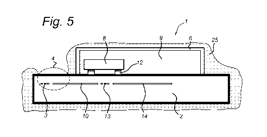
Fig. 5 shows a cross sectional view of an even further embodiment of the
present
invention optical assembly 1. In this embodiment, the optical assembly 1 is an
active implantable
medical device (AIMD), which is an active device which may be introduced in
the body of living
creatures, such as a plant or an animal or a human being. In such an
application, the AIMD is
arranged to have a direct contact with body fluids such as blood, interstitial
fluid, saliva, aqueous
humour, amniotic fluid, etc. In some embodiments, the optical assembly 1 is
arranged as an
optical sensor for sensing glucose, or alternatively/additionally for other
substances, such as urea,
lactate, creatinine, triglyceride, protein, cholesterol, ethanol, ketones and
hormones. Implants
used in a body of living creatures do not have any sharp edges or corners,
because they can
cause internal injury. In this further embodiment, the optical assembly 1
comprises a protection
layer 25 around (i.e. surrounding) the optical assembly 1. Optionally an
aperture for the optical
interaction area 4 is provided. The protection layer 25 can have e.g. a micro
structured surface or
a smooth and rounded outer surface. The protection layer 25 for example can be
a polymer layer
which can be coated after the hermetic sealing of the optical assembly 1. The
protection layer 25
can be designed and applied efficiently in such a way that the optical
interaction area 4 is kept
open to have a direct exposure to the sensing environment. Optionally, the
optical interaction area
4 can be provided with a thin anti-corrosive top layer, with a predetermined
thickness so as not
to affect the sensing and being for example in one or more materials from the
group of Silicon
Carbide (SiC), Diamond Like Carbon (DLC), TiO2, or A1203
It is an advantage of this embodiment that it allows miniaturisation of the
optical assembly
1. The miniaturization enables the optical assembly 1 to be as compact that
the natural flow of
bodily fluids or the natural diffusion of a substance, e.g. present in living
creatures enables the
possibility for sensing and for continuous monitoring of the substance. The
sensing can be
CA 03056519 2019-09-13
WO 2018/185032 PCT/EP2018/058325
9
performed e.g. using optical characterization techniques which do not require
reagents or other
auxiliary substances. These advantages result in a reliable and long term
usable optical assembly
1 without the need for significant interference of users.
In an alternative or additional embodiment, the optical microsystem assembly 1
further
comprises an energy supply device 16 positioned within the hermetically sealed
cavity 9. An
energy supply device is used for supplying the required energy for all (opto-
)electronic
components 8, 16, 17 of the optical assembly 1 as discussed with reference to
the various
embodiments described above. The energy supply device 16 is in one specific
embodiment an
energy storage, e.g. a micro battery, or in a further specific embodiment an
energy harvesting
device. A micro battery supplies fixed energy density in a limited lifetime,
depending on the size
of micro battery and the energy demands of the (opto-)electronic components 8,
16, 17. In the
further specific embodiment, the respective power demanding components 8, 16,
17 of the optical
assembly 1 use an energy harvesting device which have longer lifetime and
which can provide
more comfort and safety compared to conventional devices. Energy harvesting
devices generate
electric energy from their surroundings through direct energy conversion; e.g.
infrared radiant
energy, thermal energy (solar¨thermal, geothermal gradients of temperature,
combustion), kinetic
energy (wind, gravity, vibration), wireless transfer energy and RF radiation
energy (inductive and
capacitive coupling, e.g. using the antenna 15 described above with reference
to the
embodiments shown in Fig. 2, 3 and 4). In the present invention embodiments,
the optical
feedthrough 10 may alternatively or additionally be used for providing optical
energy from the
outside to optoelectronic components inside the sealed cavity 9. The energy
harvesting from
human or environmental sources provide an effective alternative in case of
implanted assemblies
1, e.g. using kinetic energy from body motion.
It is noted that in the embodiments described above with reference to Fig. 1-
5, the active
component 8 may be a radiation source whose radiation is used for e.g. sensing
a substance.
The light source might be one or more broadband sources (LED, SLED), a single
narrow-band
source (e.g. a laser, such as a VCSEL, a DFB laser, a DBR laser), or an
ensemble of narrow-
band sources. The reference made to light or radiation in the present
description refers to
electromagnetic radiation. The light envisaged is radiation having a suitable
wavelength or
wavelength range for sensing a certain substance. In some embodiments light
used will be
infrared radiation, e.g. visible light radiation, near IR radiation or mid IR
radiation. The fabrication
and integration technologies for the silicon photonics are well developed in
the telecommunication
wavelengths (1310nm, 1550 nm) which could be exploited for extending to the
wavelength range
of interest with easy, reliable and cost-effective manufacturing of the
present invention optical
assembly 1.
Additionally photodetectors may be integrated on the surface 5 within the
sealed cavity 9
provided by the hermetically sealed cover cap 6. The photodetectors are used
to convert the
optical signals into electrical signals. The photodetector might be a
photodiode or a
CA 03056519 2019-09-13
WO 2018/185032 PCT/EP2018/058325
photoconductor, or an ensemble of these elements. There may be additional
electronic
components 16, 17 integrated within the hermetic sealing such as a monitor
photodiode, a
wireless module or even an amplifier.
The often bulky electronic and optoelectronic components 8, 16, 17 as
described above
5 are
integrated to the substrate 2 and electrically connected to the metal bond
pads on the surface
5. The integration of the components 8, 16, 17 can be for example
monolithically, heterogeneously
or by a hybrid method. Monolithic integration is the integration technology
that uses a single
processing flow to process the diverse components potentially using different
materials, e.g.
integrated germanium detectors in silicon photonics IC. Heterogeneous
integration is the
10
integration technology for which the components are processed in separate
process flows, which
are then integrated at die or wafer level, e.g. BCB bonding, wafer bonding,
and other bonding
schemes, 3D integration. Hybrid integration is the integration of components
or materials on
processed photonic integrated platforms, e.g. flip-chipping of detectors,
bumping, gluing, wire
bonding, co-packaging, etc.
The present invention in a further aspect relates to a method for
manufacturing an optical
assembly, e.g. an optical assembly 1 according to any one of the embodiments
described herein.
The method comprises providing a substrate 2 with an integrated optical
microstructure 3 forming
an optical interaction area 4, and providing at least one active component 8
on a surface 5
adjacent to the optical interaction area 4. The method further comprises
providing a cover cap 6
on a part of the substrate 2 to form a sealed cavity 9 where at least one
active component 8 is
positioned. As discussed above the method of manufacturing the optical
assembly 1 may further
comprise providing at least one optical feedthrough 10 extending from the
sealed cavity 9 to the
exposed optical interaction area 4. In a further embodiment, the method of
manufacturing the
optical microsystem assembly 1 further comprises providing at least one
electrical feedthrough
20 extending from inside the sealed cavity 9 to an area outside of the sealed
cavity 9 in substrate
2. As discussed above referring to the embodiment shown in Fig. 5, the method
of manufacturing
the optical microsystem assembly 1 may further comprise providing a protection
layer 25 around
the optical assembly 1, possibly with an aperture for the optical interaction
area 4.
Hermetic sealing of the optical assembly 1 embodiments as described herein may
be
performed at a die or at a wafer level. Die level sealing requires individual
process for each die
and optical assembly 1, which increases packaging cost and labour time and
decreases the
process yield and reliability. On the other hand, wafer level hermetic sealing
provides a better
solution in all the above aspects by using well-known techniques, such as thin
film encapsulation
or wafer-to-wafer bonding, providing low-cost packaging solutions. Hermetic
sealing by wafer-to-
wafer bonding employs a separate cap wafer for the sealing purposes, which
provides perfect
mechanical robustness for the protection of the sensors. In an alternative or
additional
embodiment, the method of manufacturing the optical microsystem assembly 1
further comprises
sealing the cover cap 6 to the substrate 2 by a wafer-level packaging
technology (WLP).
CA 03056519 2019-09-13
WO 2018/185032 PCT/EP2018/058325
11
The present invention has been described above with reference to a number of
exemplary
embodiments as shown in the drawings. Modifications and alternative
implementations of some
parts or elements are possible, and are included in the scope of protection as
defined in the
appended claims.