Note: Descriptions are shown in the official language in which they were submitted.
CA 03060017 2019-10-15
- 1 -
Method for producing a solder connection
The present invention relates to a method for producing a solder connection
between a plurality of components in a process chamber sealed off from its
surroundings by heating and melting solder material which is arranged between
s the components to be connected.
BACKGROUND OF THE INVENTION
The term "components" is taken generally to mean circuit carriers, substrates,
substrate carriers, base plates, workpiece carriers, mounting carriers or the
like
made from metal, ceramics, plastics or other materials or any desired
io combinations of material together with components to be fastened
thereto, such
as power semiconductor chips, (semiconductor) assemblies or the like.
A method of the type in question is in particular used in large-area soldering
operations, in which for example semiconductor components, microelectronic
components or power semiconductor chips, such as for example transistors or
is diodes on printed circuit boards, IGBTs, MOSFETs or diodes on metallised
ceramic substrates or other circuit carriers are soldered or soldered
together, or
in which metallised ceramic substrates are soldered to metallic base plates
and/or heat sinks. Printed circuit boards which are to be connected to heat
sinks
may also be soldered in a soldering apparatus of the type in question.
20 In order to achieve an optimum soldering result, effort is made to heat
the
molten solder together with the components to be connected in controlled
manner to above the melting point of the solder, also at an elevated pressure
of
greater than 1013 mbar, and then to perform cooling in controlled manner to
below the solidification point of the solder in order to connect the
components
25 together without voids.
Solder connections are generally produced in a process chamber which is
sealed off from its surroundings, in particular is evacuatable, in which is
PNK-5766W0
07.05.2018
CA 03060017 2019-10-15
- 2 -
arranged a soldering apparatus which comprises a base plate and a pressure
plate, between which is received a solder group comprising the component(s)
and the solder material. The base plate and the pressure plate are adjustable
relative to one another with regard to the spacing thereof for exerting a
pressure
s force on the solder group. At the same time, the pressure plate and/or
the base
plate may heat and/or cool the components and the solder material. To this
end,
the stated plates may be thermally coupled with appropriate heat sources
and/or heat sinks.
In general, the components and the solder material, for example in the form of
solder chips or solder powder, are assembled to form a stack before being
introduced into the process chamber.
When, as is necessary, the components are handled outside and/or within the
process chamber and also during the actual soldering operation, there is
however a risk, once the molten solder material has solidified, of the
components not being in the desired position relative to one another.
Deviations
may occur with regard both to a lateral position of the components and to the
relative spacing thereof.
US 4 801 069 A discloses a method and an arrangement for solder connecting
components in a gas atmosphere, wherein in a first step a solder chip is
positioned by means of a bonding material on a printed circuit board as
circuit
carrier and at least temporarily fastened by means of heating, and in a
subsequent step a component to be soldered is temporarily fastened to the
solder chip and the circuit carrier with a further bonding material with
application
of pressure prior to a soldering operation. The operation has multiple stages
and involves repeated heating and cooling of the components, which means
that processing is not only costly in energy terms and involves exposure to
high
thermal loads but is also relatively time-consuming. The multistage
arrangement
steps can easily result in mispositioning. The multistage nature of the method
means that it cannot be implemented under a vacuum atmosphere.
PNK-5766W0
07.05.2018
CA 03060017 2019-10-15
- 3 -
US 2009/0 085 227 Al proposes a method and an apparatus for flip chip
connection of a component to a circuit carrier, in which predefined spacing is
achieved by a mounting apparatus with a placement frame which, guided by a
vacuum suction device, places a component to be connected onto a circuit
carrier. Once the component to be connected has been positioned on the circuit
carrier by means of the placement frame, it is connected by heating a solder
powder resin located therebetween, wherein a gas atmosphere of the solder
material is formed which outgasses by convection, such that only contact
surfaces which are to be connected are soldered. Neither a bonding agent for
io temporary alignment and fastening nor further application of pressure
during
and after the joining operation are here proposed in order subsequently to
maintain a minimum spacing and orientation relative to one another.
US 5 175 410 A discloses a hold-down fixture for the electrical contact feet
of a
component to be soldered on a circuit carrier for chip-on-tape mounting,
is wherein the hold-down fixture presses contact feet projecting from the
periphery
of the component onto the surface of the circuit carrier during the soldering
operation. Outer bars are intended to press the end regions to be soldered of
the contact feet against the solder pads of the circuit carrier, while inner
bars
rest directly against the package of the component to be soldered. Only
20 selected regions of the component which are to be connected are therefore
pressed directly onto the circuit carrier, and no predefinable structural
height of
the overall solder group is made possible, so controlled soldering of regions
between the component and circuit carrier is not possible in this manner. The
hold-down fixture is only usable for components with peripheral, externally
25 located contact feet.
The problem addressed by the invention is that of providing a method of the
initially stated type in which the components may be connected together more
quickly and inexpensively and with improved dimensional accuracy.
SUBJECT MATTER OF THE INVENTION
PNK-5766W0
07.05.2018
- 4 -
The problem is solved by a method for producing a solder connection between
a plurality of components in a process chamber sealed off from its
surroundings
by heating and melting solder material which is arranged between the
components to be connected, the components to be connected being
s provisionally connected with a bonding material to form a solder group in
which
the components are fixed relative to one another in a joining position,
characterised in that the solder group is heated to an intermediate
temperature
which is lower than the melting temperature of the solder material at
atmospheric pressure, and in that the pressure in the process chamber is
io reduced to a pressure below the evaporation pressure of the bonding
material
at the intermediate temperature, such that the bonding material evaporates,
wherein the pressure in the process chamber is initially reduced to a pressure
above the evaporation pressure of the bonding material at the intermediate
temperature, such that the bonding material does not yet evaporate,
is subsequently a cleaning agent is introduced into the process chamber to
clean
the solder group, and further subsequently the pressure in the process chamber
is reduced to a pressure below the evaporation pressure of the bonding
material
at the intermediate temperature.
The invention proposes that the components to be connected are provisionally
20 connected with a bonding material to form a solder group in which the
components are fixed relative to one another in a joining position. This
prevents
the components from slipping relative to one another during assembly to form
the solder group and/or during handling of the solder group, for example on
introduction into the process chamber.
25 The components are advantageously provisionally connected by the bonding
material by adhesive forces which act at the interfaces between the bonding
material and the components or the solder material.
According to one advantageous configuration, the bonding material is selected
such that it evaporates without leaving any residue during production of the
Date Recue/Date Received 2021-01-08
- 5 -
solder connection. As a consequence, it is ensured that the quality of the
solder
connection is not impaired by any residues of the bonding material.
The bonding material may be sprayed on over a wide area before or during
positioning of the components on the workpiece carrier or purposefully
applied,
s for example in the manner of an X-Y plotter, in spots, lines or over a
wide area
to previously determined points and regions provided for this purpose of the
components, of the substrate carrier and/or of the workpiece carrier.
Application
of the bonding material is preferably automatic in order to permit high-
throughput mass production.
io The soldering method is preferably carried out with solder chips or
"preforms",
wherein it is possible to dispense with the use of soldering paste which
optionally contains flux.
According to a further advantageous configuration, at an evaporation pressure
which is lower than atmospheric pressure, the evaporation temperature of the
is bonding material is lower than the melting temperature of the solder
material at
atmospheric pressure or even at an elevated pressure of above 1013 mbar. As
a consequence, it is ensured that the bonding material can completely
evaporate even before the solder material has melted. It is not absolutely
necessary for this purpose for the evaporation temperature of the bonding
20 material at atmospheric pressure to be lower than the melting
temperature of
the solder material, it may also be higher.
A further advantageous configuration provides that the solder group is heated
to
an intermediate temperature which is lower than the melting temperature of the
solder material at atmospheric pressure or also at an elevated pressure of
25 above 1013 mbar, and that the pressure in the process chamber is reduced
to a
pressure below the evaporation pressure at the intermediate temperature, such
that the bonding material evaporates. The pressure in the process chamber
may advantageously be reduced only once the solder group has been heated to
the intermediate temperature. It is, however, also possible to reduce the
Date Recue/Date Received 2021-01-08
- 6 -
pressure even before the intermediate temperature is reached. The pressure
may be reduced continuously or in steps. It should, however, be ensured that
the bonding material has been able to evaporate before the solder material
melts.
s A further advantageous configuration provides that the pressure in the
process
chamber is initially reduced to a pressure above the evaporation pressure of
the
bonding material at the intermediate temperature, such that the bonding
material does not yet evaporate, that subsequently a cleaning agent, in
particular methanoic acid, hydrogen or a plasma, is introduced into the
process
io chamber to clean the solder group, and that subsequently the pressure in
the
process chamber is reduced to a pressure below the evaporation pressure of
the bonding material at the intermediate temperature. Introduction of a plasma
into the process chamber is in particular also taken to mean production of the
plasma in the process chamber itself, wherein a suitable substance to be
15 ionised may optionally be introduced into the process chamber. The
advantage
in this configuration is that, even during the cleaning operation, there is
still a
provisional connection between the components and/or the solder material. On
reduction of the pressure in the process chamber to a pressure below the
evaporation pressure of the bonding material at the intermediate temperature,
20 the bonding material and the cleaning material can be jointly discharged
from
the process chamber.
Alternatively, it is however also possible initially to evaporate the bonding
material and only then to introduce the cleaning agent into the process
chamber.
25 According to a further advantageous configuration, the intermediate
temperature while the pressure in the process chamber is being reduced to a
pressure below the evaporation pressure of the bonding material may be
maintained at a predetermined temperature value or within a predetermined
temperature range at least until evaporation of the bonding material is
complete.
30 The stated temperature value or the stated temperature range are always
below
Date Recue/Date Received 2021-01-08
- 7 -
the melting temperature at standard pressure or also at an elevated pressure
of
above 1013 mbar. As a consequence, the risk of bonding material still being
present on the solder group while the solder material is melting is further
reduced.
s A further advantageous configuration may provide that the bonding
material is
arranged in the region of edges and/or corners and/or the centre or in the
centre
region of the components to be connected and/or of the solder material. In
this
manner, the bonding material can be applied very simply.
An advantageous embodiment provides that the solder material melts once the
io bonding material has evaporated in order to prevent contamination of the
solder
material.
A further advantageous configuration may provide that the bonding material is
liquid or pasty and in particular comprises a terpene alcohol, in particular
isobornyl cyclohexanol. The desired liquid or pasty state of matter should
is prevail at least at room temperature and atmospheric pressure.
Suitable mixtures or solutions of various substances may also be used as the
bonding material. In particular, a filler or thickener may also be added to
the
bonding material. It should, however, be ensured that even the constituents of
the bonding material which are optionally solid at room temperature and
20 atmospheric pressure are capable of evaporating at elevated temperature
and
reduced pressure in line with the above-stated conditions before the solder
material has melted.
A further advantageous configuration provides that, at least while the solder
material is melting, the solder group is received in a soldering apparatus
25 arranged in the process chamber, wherein the soldering apparatus has a
base
plate and a pressure plate, between which is received the solder group and
which are adjustable relative to one another with regard to the spacing
thereof
for exerting a pressure force on the solder group, and has a stop apparatus
Date Recue/Date Received 2021-01-08
- 8 -
which limits the spacing between the base plate and the pressure plate to a
minimum spacing, such that, once the solder material has melted, the solder
group has a predetermined thickness. The soldering apparatus ensures that the
components and the solder material are preloaded against one another and,
once the solder material has melted, continue to be compressed, since the
molten solder material can spread further between the components and
optionally fill any small interspaces present there. The stop apparatus here
limits the extent of pressing such that, once the solder material has
solidified,
the solder group has a defined thickness or height. Dimensional accuracy is
further improved as a consequence since not only lateral shifts, but also
deviations from a predetermined thickness or height of the component
assembly can reliably be prevented. In addition, in the event of excessively
strong pressing, solder material is prevented from being squeezed out
laterally
between the components. The invention differs from conventionally used
soldering frames in that direct physical contact occurs only briefly, namely
while
the solder is in the molten state or at the onset of a solidification phase.
Permanent or mechanically fixing contact is avoided in order to avoid damaging
or stressing the material.
The stop apparatus can particularly advantageously be used in a multichamber
system for flow production. Such a system comprises at least two chambers, in
particular three chambers, for preheating, connecting and cooling. The stop
apparatus is advantageously provided at least in the cooling chamber in order
to ensure mechanical alignment during solidification of the solder. The stop
apparatus may furthermore also be used in the soldering chamber for
connecting the components and may also be used in the preheating chamber
for alignment prior to the joining operation. To this end, the stop apparatus
may
advantageously be guided through the system with a displaceable workpiece
carrier.
According to one advantageous configuration, the stop apparatus is arranged
on the base plate or the pressure plate.
Date Recue/Date Received 2021-01-08
- 9 -
According to a further advantageous configuration, the stop apparatus is
adjustable, such that the minimum spacing can be set. This permits variable
adaptation of the stop apparatus to different dimensions or to a different
number
of components to be connected.
s A further advantageous configuration provides that the stop apparatus
comprises a plurality of in particular length-adjustable stop elements. As a
consequence, it is possible to ensure that dimensional accuracy can be
maintained over the entire lateral extent of the solder group. In particular,
tilting
or tipping of the pressure and base plates relative to one another can be
io avoided.
According to one advantageous configuration, the stop elements may have an
adjusting device, in particular an adjusting thread which interacts with a
complementary adjusting device, in particular a complementary thread,
provided on the base plate or the pressure plate. The desired adjustability of
the
is stop apparatus can be straightforwardly achieved as a consequence.
A further advantageous configuration provides that the stop elements are
arranged such that, on reaching the minimum spacing, they bear with a
respective free end against a component of the solder group, against a base
frame carrying one of the components or against the base plate. If the stop
20 elements are intended to bear against a component of the solder group,
said
component should sensibly be a terminating component which as it were forms
a bottom or top of the component stack and projects laterally beyond the other
components of the solder group. The stop elements may, however, also come
to a stop against other assemblies. For instance, the stop elements which are
25 for example fastened to the pressure plate may come to a stop against a
base
frame which is used as a component carrier, or even against the base plate
itself. The base frame may, for example, carry a circuit carrier as the
terminating
component of the solder group.
Date Recue/Date Received 2021-01-08
- 10 -
Temperature management in soldering and sinter-bonding processes in
electrical engineering and electronics has a major influence on a product's
quality, reliability and service life. During the solder material cooling
phase,
solder grains or islands may be formed as hardening proceeds, wherein
material-specific characteristics such as the modulus of elasticity, the
temperature coefficient of the solder material and the grain shape alignment
of
the solder can have a substantial influence on the joint. A fatigue
characteristic
of the joint is substantially dependent on the solder grain size. It has been
found
in the context of the invention that grain size and alignment can be
purposefully
io influenced by purposeful temperature adjustment during the heating
phase but
in particular during the cooling phase. It is here desirable for temperature
adjustment to be carried out not only from beneath the components, but also
from above in order to improve process control. In this manner, any mechanical
stresses which arise between the joined parts can be reduced, alignment
improved and any tendency to warping minimised. According to an
advantageous embodiment, the base plate and/or the pressure plate is thus
heatable and/or coolable. The base plate and/or the pressure plate may for
this
purpose have a heat source and/or a heat sink which may be integrated into the
base plate or into the pressure plate. The base plate and/or the pressure
plate
may also be thermally couplable or coupled with a heat source and/or a heat
sink, for example a heating and/or cooling plate. In particular, the base
plate
and/or the pressure plate may be configured such that, in the region of a
contact area with the components, they have a temperature gradient which
makes it possible to heat and/or cool the components in such a manner that
regions close to the edge of the components have a higher temperature than
regions remote from the edge. This makes it possible for the solder material
to
solidify from the inside outwards, i.e. towards the edges. During the cooling
process, still liquid solder material can continue to flow from the outside
inwards. As a consequence, it is possible to avoid the formation of voids
and/or
cavities in the solder material due to shrinkage of the volume of the solder
material during cooling. One exemplary configuration of such a device is
Date Recue/Date Received 2021-01-08
- 11 -
disclosed in document WO 2016/091962 Al. In this manner, the temperature of
the components can be purposefully controlled from above. In this respect, in
addition to providing mechanical alignment, the pressure plate permits
temperature control by purposeful heating and/or cooling of the top of the
components. This may be utilised in particular during sintering, in particular
pressure sintering, as the joining technology, so enabling both alignment and
temperature control even after departure from the sintering press.
According to the above-stated exemplary embodiment of a temperature
adjustment function of the base plate and/or pressure plate, it is
particularly
io advantageous to carry out temperature adjustment in particular of the
pressure
plate or of surface regions of the pressure plate facing towards the top of
the
component by means of a thermofluid or by means of one or more temperature
adjustment elements. The thermofluid used may be a heatable liquid, in
particular water or a water-glycol mixture, preferably at an elevated fluid
pressure of 2-3 bar or more, in order to permit rapid heating or cooling. An
electrical temperature adjustment element, in particular an electrical heating
resistor or a Peltier cooling element or the like, may likewise advantageously
be
used. An electrical element may here for example also be used as a heater and
a cooling fluid for cooling or vice versa. A radiant heater, for example in
the form
of an infrared emitter, may likewise be used and in this manner the pressure
plate may for example be heated from above by an IR emitter, advantageously
also nonuniformly by IR spot emitters or by an IR radiation mask which only
allows IR light to pass through and impinge on the pressure plate at selected
locations. The individual heating and cooling elements may conveniently be
combined. Zone heating during different process phases and in different
regions
of the apparatus is thus possible, in order to achieve end-to-end temperature
control during the joining process both on the bottom and the top of the
components.
Projecting steps, in particular thermally conductive steps and projections,
but
also recesses and depressions, may particularly advantageously be formed on
Date Recue/Date Received 2021-01-08
- 12 -
a temperature-adjustable pressure plate in order to expose different heights
of
components to pressure and to achieve good thermal coupling. The stop
elements may to this end bear directly on the workpiece carrier or the base
plate, or on further component parts such as jigs, component frames etc. The
projections and steps of the cover plate may be spring-mounted relative to the
cover plate, such that the contact pressure of the steps relative to the
component surface is dependent on a relative spacing of the cover plate from
the component surface. In this manner, it is possible to permit early
temperature
adjustment of the component prior to maximum application of pressure,
io whereby a solder temperature can be selectively maintained in the
plasticised
or in a liquid phase before a maximum contact pressure is applied.
It is advantageously possible to provide a plurality of pressure plates, each
equipped with a stop apparatus, which are height-adjustable and displaceable
relative to the workpiece carrier either jointly or individually. Individual
components may thus be placed under pressure and contacted for temperature
adjustment purposes with a time offset. The pressure plates may in each case
define individual temperature adjustment zones or be set by a single
temperature adjustment medium or a single temperature adjustment apparatus,
such that components can be differently thermally treated from above in line
with their heat capacity. If the individual pressure plates are individually
displaceable, the contact pressure may be differently set depending on the
component group.
The stop element(s) of the stop apparatus may be provided for thermal coupling
with surface regions of the components and the dimensions and shape thereof
may be specifically configured for nonuniform input or dissipation of heat.
According to a further advantageous configuration, the soldering apparatus has
a carrier unit on which the pressure plate is directly or indirectly spring-
supported or spring-mounted. In principle, however, the base plate may
alternatively or additionally be directly or indirectly spring-supported or
spring-
mounted. Spring support or mounting in particular ensures that the stop
Date Recue/Date Received 2021-01-08
- 13 -
apparatus, in particular where a plurality of stop elements are present, can
be
uniformly supported against a corresponding opposing surface, i.e. a
component, of the base plate or against the base frame. It is additionally
ensured that an adjusting apparatus, which is provided for adjusting the
relative
position between base plate and pressure plate, does not apply an inadmissibly
high pressure force and, as a consequence, potentially damage the soldering
apparatus.
A further advantageous configuration may provide that the spring force which
the pressure plate exerts on the solder group can be set. This may for example
io proceed by interchangeable springs of different length and/or with a
different
spring constant. Adjustable springs which for example set the effective length
of
the springs may also be provided. As a consequence, the pressure force acting
on the solder group can be limited in addition to the pressure force
limitation
provided by the stop apparatus.
According to a further advantageous configuration, the base plate is
adjustable
relative to the carrier unit. It is accordingly for example possible to
support the
carrier unit on the process chamber, while the base plate can be adjusted. A
reversed solution with a stationary base plate and an adjustable pressure
plate
is, however, also conceivable.
A further advantageous configuration may provide that the side of the pressure
plate associated with the base plate is planar or has at least one projecting,
in
particular planar, step which is in contact with the solder group. The
projecting
step is advantageously smaller in cross-section, i.e. in the lateral extent
thereof,
than the solder group or the component in contact with the step, such that a
lateral temperature gradient can be produced at least in the component
directly
in contact with the step.
Use of the invention is in particular advantageous in sintering, preferably in
pressure sintering, in which permanent connection of the components may be
achieved by use of pressure at reduced temperatures. Production faults and
Date Recue/Date Received 2021-01-08
- 14 -
inadequate connections can be reduced markedly by purposefully aligning the
components relative to one another and enabling height control. In particular,
a
further purposeful temperature adjustment by means of the stop apparatus from
above, is capable of improving the joining process to the effect that further
process parameters can be purposefully influenced and optimised.
DRAWINGS
Further advantageous embodiments of the invention are revealed by the
description and the drawings.
The invention is described below on the basis of exemplary embodiments and
with reference to the drawings, in which:
Figs. 1 & 2 show schematic diagrams of solder groups in side view and in
part in plan view which are provisionally connected with a
bonding material using the method of the invention,
Fig. 3 shows a schematic pressure/temperature diagram for carrying
out the method of the invention according to a first exemplary
embodiment,
Fig. 4 shows a schematic pressure/temperature diagram for carrying
out the method of the invention according to a second exemplary
embodiment,
Fig. 5 shows a schematic temperature/time diagram for carrying out the
method of the invention according to the first and/or second
exemplary embodiment,
Figs. 6 & 7 show schematic, partially sectional side views of a
soldering
apparatus of the invention according to a first exemplary
embodiment in various adjustment positions,
Fig. 8 shows side views of various solder groups, and
Date Recue/Date Received 2021-01-08
- 15 -
Figs. 9 & 10 show schematic diagrams of a soldering apparatus of the
invention arranged in a process chamber according to a second
and a third exemplary embodiment;
Figs. 11a, b show schematic diagrams of a soldering apparatus of the
invention according to a fourth exemplary embodiment;
Figs. 12a, b show schematic diagrams of a soldering apparatus of the
invention according to a fifth exemplary embodiment;
Figs. 13a, b show schematic diagrams of a soldering apparatus of the
invention according to a sixth exemplary embodiment;
io Figs. 14a, b show schematic diagrams of a soldering apparatus of the
invention according to a seventh exemplary embodiment.
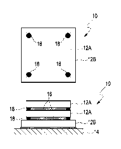
Figs. 1 and 2 show components 12A, 12B which are to be connected together
with the assistance of solder material. Solder material 16, for example in the
form of one or a plurality of solder pads, as are used, for example, in BGAs
(Ball
is Grid Arrays), is arranged in each case between components 12A and 12B.
Components 12A, 12B are in each case stacked on a further component in the
form of a circuit carrier 14, wherein a component 12B lying directly on the
circuit
carrier 14 may already in a preceding step have been connected with the
circuit
carrier 14 or solder material 16 in as yet unmelted form may likewise have
been
20 provided there.
The components 12B are identical or somewhat larger in cross-section than the
components 12A and may thus project a little beyond the latter on all sides.
The
solder material 16 arranged in the form of pads, in contrast, is somewhat
smaller in cross-section than the components 12A, such that there are
25 circumferential narrow cavities along the edges of the components 12A and
12B. In the region of the corners of the components, bonding material 18 in
the
form of small drops, which provisionally connects the components to form a
respective solder group 10, is in each case introduced into these cavities.
The
Date Recue/Date Received 2021-01-08
- 16 -
bonding material 18 is preferably liquid or pasty and in particular comprises
a
terpene alcohol, in particular isobornyl cyclohexanol. Isobomyl cyclohexanol
is
for example obtainable under the trade name "Terusolve MTPH" from Nippon
Terpene Chemicals, Inc..
The bonding material 18 fixes the components 12A, 12B relative to one another
in a joining position by adhesion, such that they are secured at least in a
lateral
direction against unintentional slipping or displacement, for example by
vibration
during transfer into a process chamber.
A solder group 10, as shown in Fig. 1 or 2, may then be introduced into a
io process chamber which may comprise a soldering apparatus. Figs. 9 and 10
show exemplary process chambers which are explained in greater detail below.
The process chamber is sealed off from its surroundings and has respective
apparatuses which are capable of modifying the pressure in the process
chamber and of respectively heating or melting the components 12A, 12B and
is the solder material 16. Further apparatuses which are capable of cooling
the
connected components 12A, 12B back down may furthermore be present in the
process chamber. Alternatively, one or more further process chambers may be
provided, into which one or more solder groups 10 may be automatically or
manually transferred for cooling and/or for further processing steps.
20 A method for producing a solder connection between the components 12A,
12B
will now be described below according to two different configurations.
The pressure/temperature diagrams (p/t diagrams) of Figs. 3 and 4 use arrows
to schematically represent changes in pressure and temperature between
various process points. A liquidus curve L represents the phase boundary
25 between the solid and liquid state of matter of the solder material 16,
for
example tin-silver-copper solder, and extends virtually independently of
pressure at a temperature of approx. 220 C. A phase boundary P indicates the
transition of the bonding material 18 from the liquid phase into the vapour
phase
Date Recue/Date Received 2021-01-08
- 17 -
as a function of temperature and pressure, wherein, above and to the left of
the
curve, the bonding material 18 is in the liquid phase and, below and to the
right
of the curve, it is in the vapour phase.
For isobornyl cyclohexanol as the bonding material 18, on which the p/t
diagrams shown are based, the boiling point at atmospheric pressure is
between 308 C and 313 C. The boiling point of the bonding material can be
reduced to below the melting point of the solder material by reducing the
pressure in the process chamber. This makes it possible to heat the solder
group 10 to close to the melting point of the solder material 16 without the
io bonding material 18 already evaporating.
Starting from a process point A, at which atmospheric pressure and room
temperature prevail, initially only the temperature is raised until, at a
process
point B, a temperature of approx. 180 C is reached.
In the exemplary embodiment according to Fig. 3, in a subsequent step the
is pressure in the process chamber is then reduced until a process point C at
180 C and a pressure between 1 and 10 mbar is achieved. The phase
boundary P is crossed during the transition from process point B to process
point C, such that the bonding material 18 evaporates and can be discharged
from the process chamber.
20 A cleaning agent, for example methanoic acid or hydrogen may then be
introduced into the process chamber or a plasma may be introduced or
produced in order to clean the components 12A, 12B to be connected.
In a following step, the temperature may then be raised from 180 C to the
melting temperature of the solder material 16 of 220 C or above, such that
25 process point D is reached.
In the second exemplary embodiment according to Fig. 4, at variance with the
first exemplary embodiment according to Fig. 3, once process point B is
reached the pressure is simply reduced until a process point B' is reached
Date Recue/Date Received 2021-01-08
- 18 -
which is still just above the phase boundary P of the bonding material 18,
i.e.
still within the liquid phase of the bonding material. Process point B' is for
example located at a temperature of 180 C and a pressure between 10 and
100 mbar.
s When process point B' is reached, cleaning agent is, as previously
described,
introduced into the process chamber in order to clean the components 12A, 12B
of contamination. In contrast with the first exemplary embodiment, the bonding
material 18 does not yet evaporate at process point B'. Once cleaning is
complete, the pressure is further reduced at largely constant temperature
until
io process point C with a temperature of 180 C and a pressure of between 1
and
mbar is reached. The bonding material 18 now begins to evaporate and,
together with the cleaning agent, is discharged from the process chamber.
Under approximately constant pressure, the temperature of the solder group 10
is then raised until, at process point D, the liquidus curve L is reached or
is crossed and the solder material 18 melts and connects with the components
12A, 12B.
It should be noted at this point that the transition between the various
process
points A, B, B', C and D is only schematic. Temperature and pressure may
accordingly at least in places also be simultaneously changed, such that
states
need not necessarily change isothermally or isobarically. However, prior to
establishing the conditions which bring about evaporation of the bonding
material 18, efforts are made to bring the temperature of the solder group 10
as
close as possible to the liquidus temperature of the solder material 16 in
order
as far as possible to minimise the period of time during which the bonding
material 18 has already evaporated but the components are not yet connected.
It furthermore goes without saying that pressure deviations may also occur
during the process which are caused by evaporation of bonding material 18
and/or solvents or cleaning agents, since any gas which arises can only be
Date Recue/Date Received 2021-01-08
- 19 -
cleared from the process chamber by the corresponding vacuum devices of the
process chamber with a time delay.
Fig. 5 shows an exemplary temperature/time diagram, on which the time profile
of the solder group temperature is indicated by a temperature curve T.
s The soldering process may be subdivided into various process phases P1 to
P4
which are indicated accordingly in Fig. 5. Various regions or time periods in
which specific atmospheric states prevail in the process chamber are
furthermore indicated in the diagram. Regions in which a nitrogen atmosphere
is present are indicated with reference sign N, regions in which a vacuum
(with
io different pressures) prevails are indicated with the reference sign V
and a
region in which a cleaning agent atmosphere is present is indicated with the
reference sign R.
During a preheating phase P1, the temperature of the solder group is raised to
160 C to 180 C. A nitrogen atmosphere N is present for most of the duration of
is the preheating phase P1, wherein a vacuum V is briefly created at the end
of
the preheating phase P1.
Cleaning phase P2 then follows, in which a cleaning agent atmosphere R
prevails and a vacuum V is produced just for a short time at the end. This
short
vacuum phase indicates the discharge of the evaporated bonding material or
20 cleaning agent. The temperature changes only slightly during the
cleaning
phase P2.
The preheating phase P1 and the cleaning phase P2 advantageously proceed
in a first chamber (preheating chamber) of a multichamber system.
Then, during melting phase P3, the temperature rises to the melting
25 temperature of the solder material of approx. 220 C, wherein a nitrogen
atmosphere N is initially present which, once the melting temperature is
reached, is replaced by a vacuum V. At the end of the melting phase P3,
nitrogen is again introduced into the process chamber, wherein this nitrogen
Date Recue/Date Received 2021-01-08
- 20 -
atmosphere N is also maintained during the subsequent cooling phase P4, in
which the temperature is reduced to below 50 C.
The melting phase P3 advantageously proceeds in a second chamber
(soldering chamber) and the cooling phase P4 in a third chamber (cooling
s chamber), wherein the two phases P3 and P4 may also proceed in a single
chamber.
The individual chambers may advantageously be separated from one another in
gas-tight manner and a conveying device for passing the workpiece carriers
through the individual chambers is provided, such that higher throughput can
be
io achieved in flow production.
A soldering apparatus 50 of the invention according to a first exemplary
embodiment is described below with reference to Figs. 6 and 7. The stop
apparatus described below is advantageously used at least in the cooling
chamber during cooling phase P4 while the solder is still liquid. A contact
is pressure may here act on the top of the components.
The soldering apparatus 50 comprises a base frame 54 and a carrier unit 52
connected with the base frame 54. A substrate 14 of a solder group 10 is
placed
in the base frame 54 and is preloaded towards the base frame 54 by pressure
springs 72 which bear against the carrier unit 52. A pressure plate 64 is
spring-
20 mounted by means of pressure springs 70 on the carrier unit 52. The
pressure
plate 64 has a stop apparatus with a plurality of stop elements 68 which are
length-adjustably fastened to the pressure plate 64 by means of adjusting
threads. A spring-loaded temperature sensor which can measure the
temperature of the substrate 14 is integrated in a through-hole in the base
plate
25 66.
Once the solder group 10 has been placed in the base frame 54 and the carrier
unit 52 fastened to the base frame 54, the unit comprising carrier unit 52 and
Date Recue/Date Received 2021-01-08
- 21 -
base frame 54 can be inserted into a retaining unit 56, wherein the base frame
54 is fixed by means of guide rollers 58, 60 and retaining strips 62.
The soldering apparatus 50 furthermore comprises a height-adjustable base
plate 66 which can come into direct contact with the substrate 14 through the
s base frame 54 which is open at the bottom.
The soldering apparatus 50 may be arranged, as will be explained in greater
detail below, in an evacuatable process chamber.
The base plate 66 and/or the pressure plate 64 may be connected with heat
sources and/or heat sinks (not shown) which make it possible to heat or cool
io the solder group 10. If the base plate 66 is adjusted in the direction
of the arrow
(Fig. 7) towards the pressure plate 64, the circuit carrier 14, including the
components 12A, 12B mounted thereon, is lifted out of the base frame 54
against the force of the pressure springs 72. After a specific adjustment
travel,
the upper component 12B comes into contact with the pressure plate 64A such
is that a pressure force is applied to the solder group 10 and the
components 12A,
12B or the circuit carrier 14 are compressed until the free end of the stop
elements 68 comes into contact with the circuit carrier 14. In this position
shown
in Fig. 7, the pressure plate 64 and the base plate 66 have reached their
minimum spacing, such that the solder group 10 can be no further compressed.
20 As a consequence, it is possible according to Fig. 8 to create a solder
group 10
which has a defined height h.
If, instead of the circuit carrier 14, an auxiliary carrier plate (not shown)
is placed
in the base frame 54, on which one or more components 12A, 12B are merely
laid without solder material and in turn solder material 16 is laid on the
25 components 12A, 12B, these components 12A, 12B can be provided, before a
solder connection is actually produced, with a coating of melted solder
material
16 which likewise has a defined height h (see Fig. 8). The pressure plate 64
may for this purpose be provided with a release agent coating at the contact
point with the solder material 16.
Date Recue/Date Received 2021-01-08
- 22 -
Soldering apparatuses 150, 250 according to a second or third exemplary
embodiment will now be described with reference to Figs. 9 and 10
respectively.
The soldering apparatuses 150, 250 comprise an evacuatable process chamber
74 which is sealed off from its environment. In the process chamber 74, an
only
schematically represented retaining unit 56 is shown which receives or mounts
a base frame 54. A circuit carrier 14 as a component part of two solder groups
is in turn mounted in the base frame 54.
The soldering apparatus 150 (Fig. 9) comprises a pressure plate 64 which is
mounted on the process chamber 74.
io The soldering apparatus 250 (Fig. 10) comprises a pressure plate 64 which
is
mounted on the base frame 54 in a similar manner as in the first exemplary
embodiment (Figs. 6 and 7).
The soldering apparatuses 150, 250 further comprise a height-adjustable base
plate 66 which may come into contact with the substrate through an opening in
the base frame 54. The substrate with the two solder groups 10 may here be
pressed against the pressure plate 64. On the pressure plate 64 are fastened
stop elements 68 which, once a minimum spacing between the base plate 66
and the pressure plate 64 has been reached, bear on the circuit carrier 14,
such
that the solder groups 10 are no further compressed and thus have a defined
height.
The stop elements 68 may here also be of height-adjustable construction.
The pressure plate 64 may be planar (Figs. 6, 7 and 10) or according to a
variation have one or more projecting steps 76 which come into contact with
the
solder groups 10 (Fig. 9). The steps 76 may, as shown in Fig. 9, have a
somewhat smaller cross-section such that they only come into contact with part
of the surface of the uppermost component. As a consequence, a temperature
gradient can be produced within the components.
Date Recue/Date Received 2021-01-08
- 23 -
Advantageously, various selective cooling concepts in the context of
horizontal
alignment may be achieved by the pressure plate. Selective cooling on
completion of the soldering operation is known in the prior art, for instance
concepts involving exposing a soldered item to coolant vapour from the bottom
or mechanically contacting it with cooling pins. It is thus ensured that,
during the
solidification process, the soldering agent solidifies in defined manner from
the
inside outwards and thus no voids and defects are formed in the solder's
microstructure. The remaining Figs. 11 to 14 (in each case with distant and
applied pressure plate) show various concepts for mechanically contacting a
io cooling or heating device with the top of a component in order to permit
selective control of heating or cooling in such a way that the solidification
process of the soldering agent can also be selectively influenced from above
by
mechanical connection by the pressure plate.
Figs. 11 to 14 show different embodiments which illustrate various options for
selectively cooling or heating solder groups uniformly or nonuniformly from
the
top:
In Fig. 11a (with spaced pressure plate 64), a step 76 of the pressure plate
64,
which step is coolable or heatable, is being advanced towards a solder group
10 of stacked components 12 which are connected by means of solder material
16, see Fig. 11b, in order to provide cooling/heating from above. Compression
travel is limited by stop elements 68 which bear on the top of a component
frame 82 or jig. The stop plate 64 is guided by a pressure apparatus retaining
frame 84 which serves as a frame for the pressure plate 64, wherein the
retaining frame 84 may be alternatively heated or cooled by means of ports 78
for a thermofluid. The thermofluid may be a pressurised water and glycol
mixture which allows the temperature of the pressure plate to be rapidly set.
The base plate 66, which carries the circuit carrier 14, may likewise be
heated
or cooled by a thermofluid by means of ports 78, such that the temperature can
be set from both above and below. Prior to application of pressure, the solder
material 16 is nonuniformly distributed under the solder group 10, such that
the
Date Recue/Date Received 2021-01-08
- 24 -
solder group 10 is askew relative to the circuit carrier 14, resulting in a
variable
solder distribution. After application of pressure in Fig. 11b, horizontal
alignment
may be achieved and solder material uniformly distributed within and below the
solder group 10.
s In a configuration, modified relative to Fig. 11, of the exemplary
embodiment of
Fig. 12a (spaced pressure plate 64) and Fig. 12b (application of pressure onto
the solder group 10), an overall solder group 10 comprising a plurality of
components 12a to 12d is compressed by a single pressure plate 64. The
temperature of the pressure plate 64 is in turn adjusted by a retaining frame
84
io through which fluid is passed and the temperature of the base plate 66
arranged beneath the solder group 10 may likewise be adjusted via the circuit
carrier 14. The solder group includes a plurality of adjacent components 12c,
12d which are sandwiched by larger components 12a, 12b as base and cover.
Aligning the larger components 12a, 12b, for example cooling plate and
15 backplane, aligns the smaller components 12c, 12d.
In the embodiment of a stop apparatus shown in Figs. 13a, 13b (in respectively
open and compressed representation), a plurality of pressure plates 64a, 64b
are provided which may be separately and individually displaced but may also
be jointly displaced on a retaining frame 84. The pressure plates 64a, 64b in
20 each case comprise individually settable pressure elements 68, which may
for
example have different heights and are separately or jointly temperature-
adjustable by means of fluid ports 78. Thanks to steps 76, different solder
groups 10a, 10b can be compressed on a substrate carrier 14 in a manner
adapted to the height and size of the surface. In this manner, soldered items
10
25 of differing heights can be selectively cooled and aligned. Heating or
cooling
capacity can be individually set on different pressure elements. The various
stop elements 76 ensure individually settable stop heights of the pressure
plates 64a, 64b.
Finally, the embodiment represented in Figs. 14a, 14b (open and compressed
30 state) shows a pressure plate 64 without its own cooling or heating
device. The
Date Recue/Date Received 2021-01-08
- 25 -
temperature of the pressure plate 64 can be indirectly adjusted via a
laterally
arranged cooling or heating device which is integrated in a retaining frame 84
of
the pressure plate 64. The pressure plate 64 may accordingly for example be
integrated in a hold-down device and/or may have its temperature adjusted by a
cooling or heating device arranged beneath the soldered item. Vertical steps
76
are arranged on the pressure plate which are capable of selectively bearing on
individual surface regions of the solder group 10 and are capable of
selectively
introducing or removing heat. The steps 76 simultaneously serve as stop
elements 68. Individual components 12a may here be compressed and
io temperature-adjusted while other, pressure-sensitive components 12b, 12c of
the solder group 10 are left free.
The embodiments shown in Figs. 11-14 may be used individually or in
combination and may synergistically complement and be combined with one
another or individually exert their advantageous effect.
In all the embodiments of the soldering apparatus 50, 150, 250 (Figs. 6 to
14),
the components 12A, 12B may be provisionally connected by means of bonding
material 18 with one another, with the solder material 16 and/or with the
circuit
carrier or substrate 14 in the manner described with reference to Figs. 1 to
5.
Date Recue/Date Received 2021-01-08
CA 03060017 2019-10-15
- 26 -
List of reference signs
Solder group
12A, 12B Component
5 14 Substrate/circuit carrier
16 Solder material
18 Bonding material
50, 150, 250 Soldering apparatus
52 Carrier unit
10 54 Base frame
56 Retaining unit
58, 60 Guide roller
62 Retaining strip
64 Pressure plate
66 Base plate
68 Stop element
70, 72 Pressure spring
74 Process chamber
76 Step
zo 78 Temperature-adjustment fluid port
82 Component frame
84 Pressure apparatus retaining frame
A, B, B', C, D Process point
L Liquidus curve
N Nitrogen atmosphere
P Phase boundary
P1 Preheating phase
P2 Cleaning phase
P3 Melting phase
P4 Cooling phase
PNK-5766W0
07.05.2018
CA 03060017 2019-10-15
- 27 -
R Cleaning agent atmosphere
T Temperature curve
V Vacuum
PNK-5766W0
07.05.2018